

Page 1
1
®
BUF600, 601
HIGH-SPEED BUFFER AMPLIFIER
FEATURES
● OPEN-LOOP BUFFER
● HIGH-SLEW RATE: 3600V/
µs, 5.0Vp-p
● BANDWIDTH: 320MHz, 5.0Vp-p
900MHz, 0.2Vp-p
● LOW INPUT BIAS CURRENT: 0.7
µA/1.5µA
● LOW QUIESCENT CURRENT: 3mA/6mA
● GAIN FLATNESS: 0.1dB, 0 to 300MHz
The BUF601, with 6mA quiescent current and therefore lower output impedance, can easily drive 50Ω
inputs or 75Ω systems and cables.
The broad range of analog and digital applications
extends from decoupling of signal processing stages,
impedance transformation, and input amplifiers for
RF equipment and ATE systems to video systems,
distribution fields, IF/communications systems, and
output drivers for graphic cards.
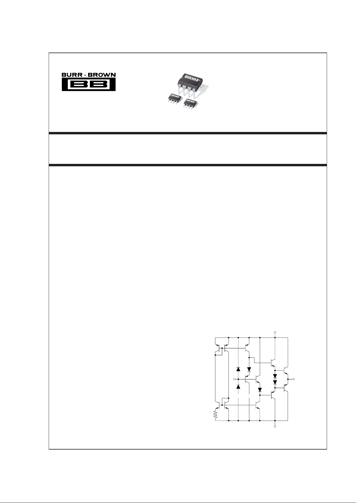
V+ = +5V
(1)
Bias
Circuitry
V
OUT
(8)
V
IN
(4)
V– = –5V
(5)
BUFFER
Simplified Circuit Diagram
BUF600
BUF601
®
DESCRIPTION
The BUF600 and BUF601 are monolithic open-loop
unity-gain buffer amplifiers with a high symmetrical
slew rate of up to 3600V/µs and a very wide bandwidth of 320MHz at 5Vp-p output swing. They use a
complementary bipolar IC process, which incorporates pn-junction isolated high-frequency NPN and
PNP transistors to achieve high-frequency performance
previously unattainable with conventional integrated
circuit technology.
Their unique design offers a high-performance alternative to expensive discrete or hybrid solutions.
The BUF600 and BUF601 feature low quiescent
current, low input bias current, small signal delay time
and phase shift, and low differential gain and phase
errors.
The BUF600 with 3mA quiescent current is wellsuited for operation between high-frequency
processing stages. It demonstrates outstanding performance even in feedback loops of wide-band amplifiers
or phase-locked loop systems.
APPLICATIONS
● VIDEO BUFFER/LINE DRIVER
● INPUT/OUTPUT AMPLIFIER FOR
MEASUREMENT EQUIPMENT
● PORTABLE SYSTEMS
● TRANSMISSION SYSTEMS
● TELECOMMUNICATIONS
● HIGH-SPEED ANALOG SIGNAL
PROCESSING
● ULTRASOUND
International Airport Industrial Park • Mailing Address: PO Box 11400, Tucson, AZ 85734 • Street Address: 6730 S. Tucson Blvd., Tucson, AZ 85706 • Tel: (520) 746-1111 • Twx: 910-952-1111
Internet: http://www.burr-brown.com/ • FAXLine: (800) 548-6133 (US/Canada Only) • Cable: BBRCORP • Telex: 066-6491 • FAX: (520) 889-1510 • Immediate Product Info: (800) 548-6132
BUF600
BUF600
BUF601
© 1991 Burr-Brown Corporation PDS-1128F Printed in U.S.A. March, 1998
Page 2
2
®
BUF600, 601
INPUT OFFSET VOLTAGE
Initial ±15 ±30 ±15 ±30 mV
vs Temperature 925µV/°C
vs Supply (tracking) V
CC
= ±4.5V to ±5.5V –54 –72 –54 –77 dB
vs Supply (non-tracking) V
CC
= +4.5V to +5.5V –55 –55 dB
vs Supply (non-tracking) V
CC
= –4.5V to –5.5V –54 –54 dB
INPUT BIAS CURRENT
Initial +3.5 –2.5/+5 +3.5 –5/+10 µA
vs Temperature 0.4 0.7 nA/°C
vs Supply (tracking) V
CC
= ±4.5V to ±5.5V 0.15 0.3 µA/V
vs Supply (non-tracking) V
CC
= +4.5V to +5.5V 0.5 0.5 µA/V
vs Supply (non-tracking) V
CC
= –4.5V to –5.5V 20 20 nA/V
INPUT IMPEDANCE 4.8 || 1 2.5 || 1 MΩ || pF
INPUT NOISE
Voltage Noise Density f = 100kHz to 100MHz 5.2 4.8 nV/√Hz
Signal-to-Noise Ratio S/N = 20 Log (0.7/(Vn • √5MHz)) 95 96 dB
TRANSFER CHARACTERISTICS Voltage Gain; V
IN
= ±2.5V
R
LOAD
= 100Ω 0.95 V/V
R
LOAD
= 200Ω 0.96 V/V
R
LOAD
= 10kΩ 0.99 0.99 V/V
RATED OUTPUT
Voltage Output V
IN
= ±2.7V
R
LOAD
= 100Ω±2.5 ±2.6 V
R
LOAD
= 200Ω±2.5 ±2.6 V
DC Current Output DC, R
LOAD
= 100Ω±20 ±20 mA
Output Impedance 6.2 3.6 Ω
POWER SUPPLY
Rated Voltage ±5 ±5V
Derated Performance ±4.5 ±5.5 ±4.5 ±5.5 V
Quiescent Current ±2.6 ±3 ±3.4 ±5.4 ±6 ±6.6 mA
TEMPERATURE RANGE
Specification –40 85 –40 85 °C
Storage –40 125 –40 125 °C
BUF600AP, AU BUF601AU
PARAMETER CONDITIONS MIN TYP MAX MIN TYP MAX UNITS
AC SPECIFICATION
At VCC = ±5V, R
LOAD
= 200Ω (BUF600) and 100Ω (BUF601), R
SOURCE
= 50Ω, and T
AMB
= +25°C, unless otherwise noted.
FREQUENCY DOMAIN
LARGE SIGNAL BANDWIDTH V
O
= 5Vp-p, C
OUT
= 1pF 320 320 MHz
(–3dB) V
O
= 2.8Vp-p, C
OUT
= 1pF 400 400 MHz
V
O
= 1.4Vp-p, C
OUT
= 1pF 700 700 MHz
SMALL SIGNAL BANDWIDTH V
O
= 0.2Vp-p, C
OUT
= 1pF 650 900 MHz
GROUP DELAY TIME 250 200 ps
DIFFERENTIAL GAIN V
IN
= 0.3Vp-p, f = 4.43MHz
V = 0 to 0.7V
BUF600 R
LOAD
= 200Ω 0.5 %
R
LOAD
= 1kΩ 0.075 %
BUF601 R
LOAD
= 100Ω 0.4 %
R
LOAD
= 500Ω 0.05 %
DIFFERENTIAL PHASE V
IN
= 0.3Vp-p, f = 4.43MHz
V = 0 to 0.7V
BUF600 R
LOAD
= 200Ω 0.02 Degrees
R
LOAD
= 1kΩ 0.04 Degrees
BUF601 R
LOAD
= 100Ω 0.025 Degrees
R
LOAD
= 500Ω 0.03 Degrees
SPECIFICATIONS
DC SPECIFICATION
At VCC = ±5V, R
LOAD
= 10kΩ, R
SOURCE
= 50Ω, and T
AMB
= +25°C, unless otherwise noted.
BUF600AP, AU BUF601AU
PARAMETER CONDITIONS MIN TYP MAX MIN TYP MAX UNITS
Page 3
3
®
BUF600, 601
BUF600AP, AU BUF601AU
PARAMETER CONDITIONS MIN TYP MAX MIN TYP MAX UNITS
HARMONIC DISTORTION
Second Harmonic f = 10MHz, V
O
= 1.4Vp-p –65 –65 dBc
Third Harmonic –64 –67 dBc
Second Harmonic f = 30MHz, V
O
= 1.4Vp-p –51 –59 dBc
Third Harmonic –56 –62 dBc
Second Harmonic f = 50MHz, V
O
= 1.4Vp-p –43 –53 dBc
Third Harmonic –48 –54 dBc
GAIN FLATNESS PEAKING
V
O
= 0.4Vp-p, DC to 30MHz 0.01 0.005 dB
V
O
= 0.4Vp-p, 30MHz to 300MHz 0.3 0.1 dB
LINEAR PHASE DEVIATION
V
O
= 0.4Vp-p, DC to 30MHz 5.5 3.8 Degrees
V
O
= 0.4Vp-p, 30 to 300MHz 55 45 Degrees
TIME DOMAIN
RISE TIME 10% to 90%, 700ps
1.4Vp-p Step 0.82 0.87 ns
2.8Vp-p Step 0.97 0.95 ns
5.0Vp-p Step 1.18 1.13 ns
SLEW RATE
V
O
= 1.4Vp-p 1500 1500 V/µs
V
O
= 2.8Vp-p 2400 2400 V/µs
V
O
= 5.0Vp-p 3400 3600 V/µs
AC-SPECIFICATIONS (CONT)
At VCC = ±5V, R
LOAD
= 200Ω (BUF600) and 100Ω (BUF601), R
SOURCE
= 50Ω, and T
AMB
= +25°C, unless otherwise noted.
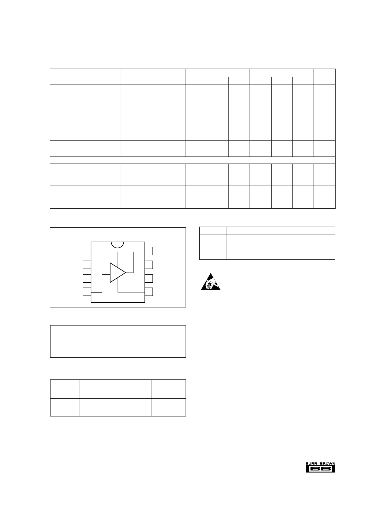
PIN CONFIGURATION
Top View
DIP/SO-8
FUNCTION DESCRIPTION
In Analog Input
Out Analog Output
+V
CC
Positive Supply Voltage; typical +5VDC
–V
CC
Negative Supply Voltage; typical –5VDC
FUNCTIONAL DESCRIPTION
ELECTROSTATIC
DISCHARGE SENSITIVITY
This integrated circuit can be damaged by ESD. Burr-Brown
recommends that all integrated circuits be handled with
appropriate precautions. Failure to observe proper handling
and installation procedures can cause damage.
ESD damage can range from subtle performance degradation to complete device failure. Precision integrated circuits
may be more susceptible to damage because very small
parametric changes could cause the device not to meet its
published specifications.
Power Supply Voltage.......................................................................... ±6V
Input Voltage
(1)
.........................................................................±VCC ±0.7V
Operating Temperature..................................................... –40°C to +85 °C
Storage Temperature...................................................... –40°C to +125°C
Junction Temperature .................................................................... +150°C
Lead Temperature (soldering, 10s)................................................ +300°C
NOTE: (1) Inputs are internally diode-clamped to ±V
CC.
ABSOLUTE MAXIMUM RATINGS
PACKAGE
DRAWING TEMPERATURE
PRODUCT PACKAGE NUMBER
(1)
RANGE
BUF600AP Plastic 8-Pin DIP 006 –40°C to +85°C
BUF600AU SO-8 Surface Mount 182 –40°C to +85°C
BUF601AU SO-8 Surface Mount 182 –40°C to +85°C
NOTE: (1) For detailed drawing and dimension table, please see end of data
sheet, or Appendix C of Burr-Brown IC Data Book.
PACKAGE/ORDERING INFORMATION
1
2
3
4
8
7
6
5
+V
CC
NC
NC
In
Out
NC
NC
–V
CC
BUF600, BUF601
The information provided herein is believed to be reliable; however, BURR-BROWN assumes no responsibility for inaccuracies or omissions. BURR-BROWN assumes
no responsibility for the use of this information, and all use of such information shall be entirely at the user’s own risk. Prices and specifications are subject to change
without notice. No patent rights or licenses to any of the circuits described herein are implied or granted to any third party. BURR-BROWN does not authorize or warrant
any BURR-BROWN product for use in life support devices and/or systems.
Page 4
4
®
BUF600, 601
INPUT PROTECTION
Static damage has been well recognized for MOSFET devices, but any semiconductor device deserves protection
from this potentially damaging source. The BUF600 and
BUF601 incorporate on-chip ESD protection diodes as shown
in Figure 1. This eliminates the need for the user to add
external protection diodes, which can add capacitance and
degrade AC performance.
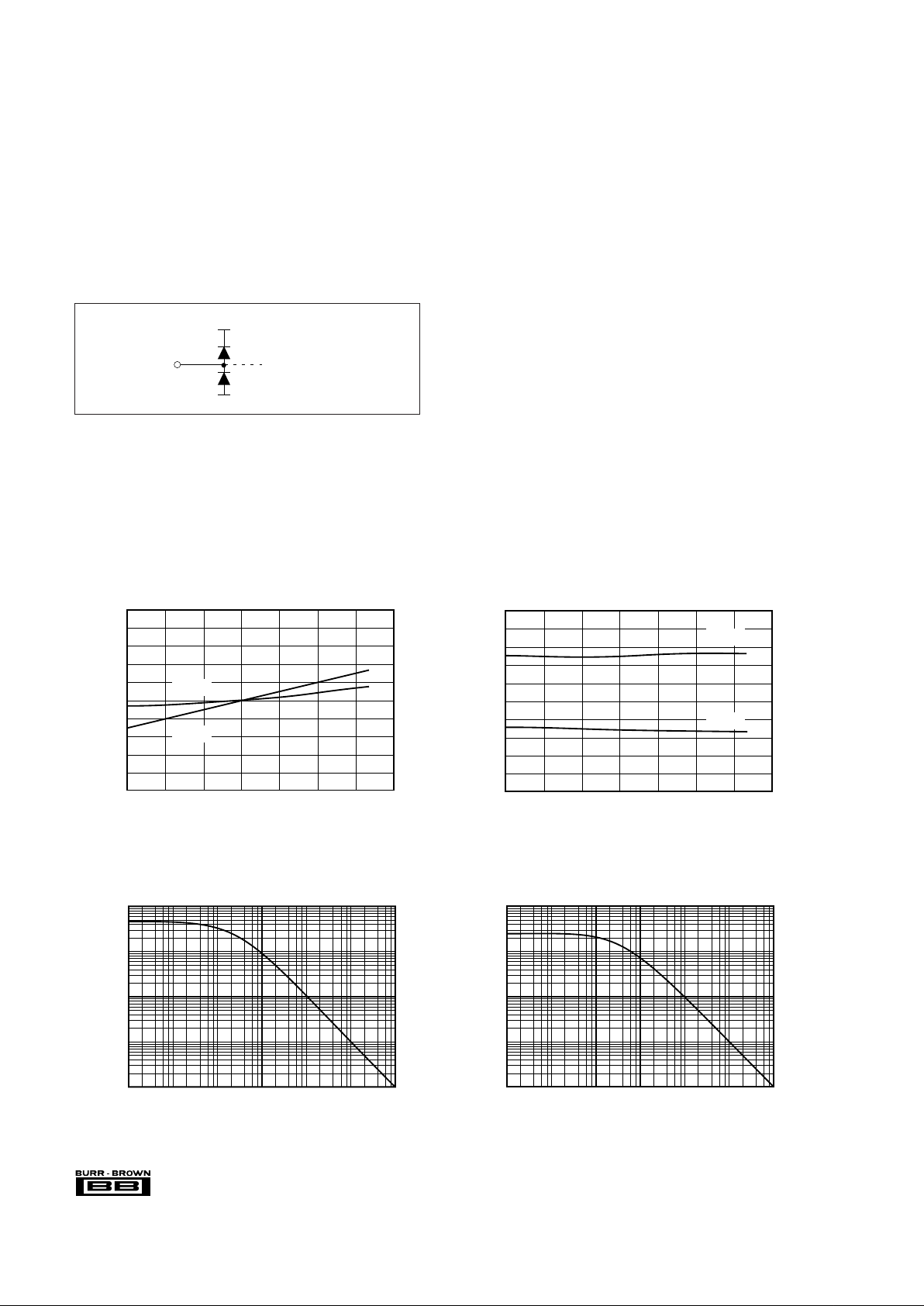
FIGURE 1. Internal ESD Protection.
+V
CC
–V
CC
External
Pin
Internal
Circuitry
ESD Protection Diodes
internally connected to
all pins.
All input pins on the BUF600 and BUF601 are internally
protected from ESD by means of a pair of back-to-back
reverse-biased diodes to the power supplies as shown. These
diodes will begin to conduct when the input voltage exceeds
either power supply by about 0.7V. This situation can occur
with loss of the amplifier’s power supplies while a signal
source is still present. The diodes can typically withstand a
continuous current of 30mA without destruction. To insure
long term reliability, however, the diode current should be
externally limited to 10mA or so whenever possible.
The internal protection diodes are designed to withstand
2.5kV (using the Human Body Model) and will provide
adequate ESD protection for most normal handling procedures. However, static damage can cause subtle changes in
amplifier input characteristics without necessarily destroying the device. In precision amplifiers, this may cause a
noticeable degradation of offset and drift. Therefore, static
protection is strongly recommended when handling the
BUF600 and BUF601.
TYPICAL PERFORMANCE CURVES
At VCC = ±5V, R
LOAD
= 10kΩ, and TA = 25°C, unless otherwise noted.
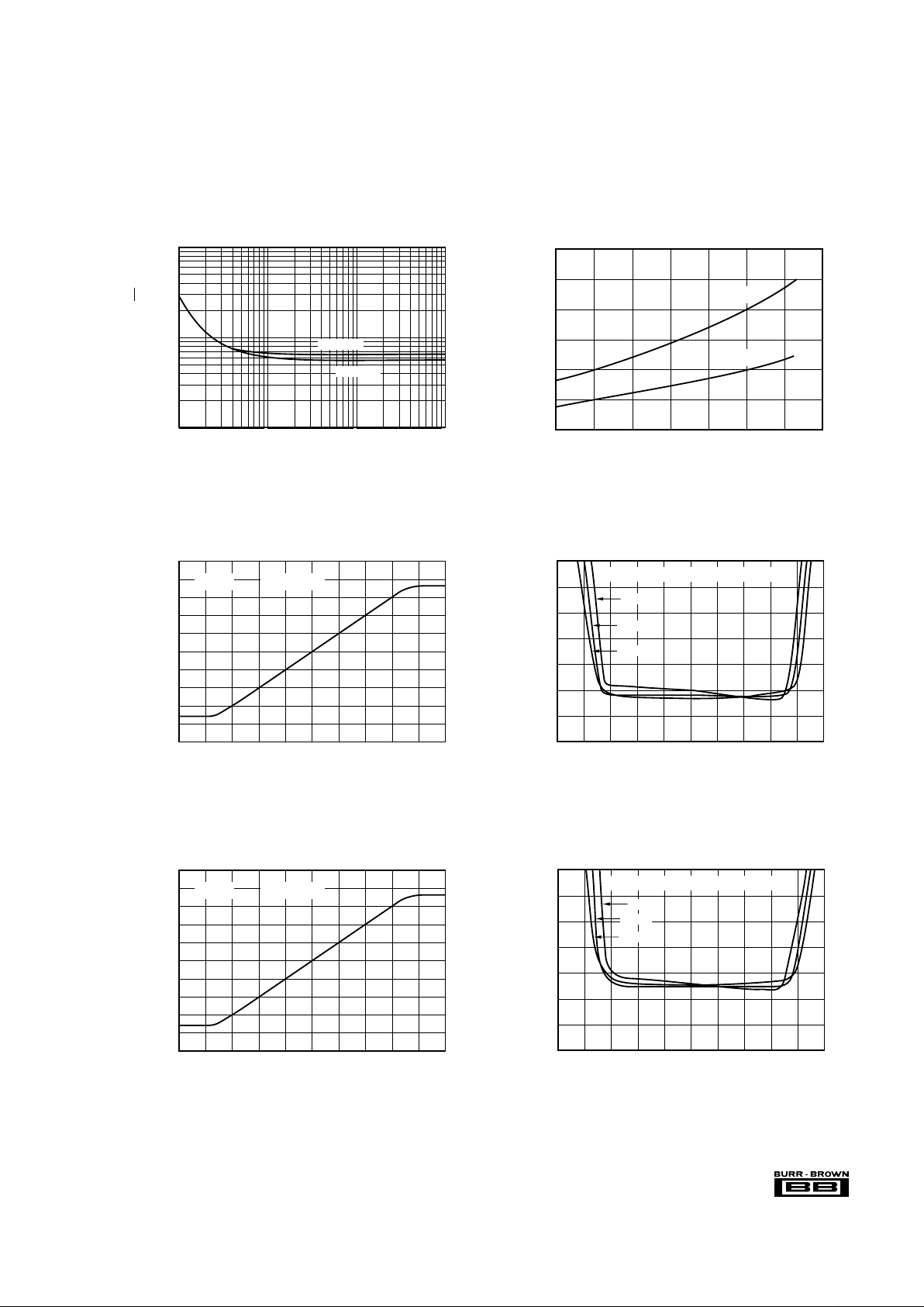
INPUT BIAS CURRENT vs TEMPERATURE
–40
2
1.8
1.6
1.4
1.2
1
0.8
0.6
0.4
0.2
0
Temperature (°C)
Bias Current (µA)
–200 20406080100
BUF600
BUF601
OFFSET VOLTAGE vs TEMPERATURE
–40
5
4
3
2
1
0
–1
–2
–3
–4
–5
Temperature (°C)
Offset Voltage (mV, normalized)
–200 20406080100
BUF600
BUF601
INPUT IMPEDANCE vs FREQUENCY BUF601
100
10M
1M
100k
10k
1k
Frequency (Hz)
Input Impedance (Ω)
1k 10k 100k 1M 10M 100M
INPUT IMPEDANCE vs FREQUENCY BUF600
100
10M
1M
100k
10k
1k
Frequency (Hz)
Input Impedance (Ω)
1k 10k 100k 1M 10M 100M
Page 5
5
®
BUF600, 601
TYPICAL PERFORMANCE CURVES (CONT)
At VCC = ±5V, R
LOAD
= 10kΩ, and TA = 25°C, unless otherwise noted.
BUF601 GAIN ERROR vs INPUT VOLTAGE
–5
14
12
10
8
6
4
2
0
Input Voltage (V)
Gain Error (%)
–4 –3 –2 –1 0 1 2 3 4 5
+85°C
(Full Temperature Range, R
LOAD
= 100Ω)
–40°C
+25°C
BUF601 TRANSFER FUNCTION
–5
5
4
3
2
1
0
–1
–2
–3
–4
–5
Input Voltage (V)
–4–3–2–1012345
Output Voltage (V)
R
LOAD
= 100ΩBUF601
BUF600 GAIN ERROR vs INPUT VOLTAGE
–5
14
12
10
8
6
4
2
0
Input Voltage (V)
Gain Error (%)
–4 –3 –2 –1 0 1 2 3 4 5
85°C
(Full Temperature Range, R
LOAD
= 200Ω)
–40°C
+25°C
BUF600 TRANSFER FUNCTION
–5
5
4
3
2
1
0
–1
–2
–3
–4
–5
Input Voltage (V)
–4–3–2–1012345
Output Voltage (V)
R
LOAD
= 200ΩBUF600
INPUT VOLTAGE NOISE
SPECTRAL DENSITY BUF600/601
100
100
10
1
Frequency (Hz)
Voltage Noise (nV/√Hz)
1000 10k 100k
BUFF600
BUFF601
QUIESCENT CURRENT vs TEMPERATURE
–40
12
10
8
6
4
2
0
Temperature (°C)
Quiescent Current (mA)
–200 20406080100
BUF600
BUF601
Page 6

6
®
BUF600, 601
TYPICAL PERFORMANCE CURVES (CONT)
At VCC = ±5V, R
LOAD
= 100Ω (BUF601), R
LOAD
= 200Ω (BUF600), and TA = 25°C, unless otherwise noted.
BUF600 SMALL SIGNAL PULSE RESPONSE
160
120
80
40
0
–40
–80
–120
–160
0 5 10 15 20 25 30 35 40 45 50
Time (ns)
Voltage (mV)
V
I
VI = 0.2Vp-p
t
RISE
= t
FALL
= 3ns
(Generator)
V
O
BUF600 SMALL SIGNAL PULSE RESPONSE
160
120
80
40
0
–40
–80
–120
–160
Time (ns)
Voltage (mV)
0 5 10 15 20 25 30 35 40 45 50
VI = 0.2Vp-p
t
RISE
= t
FALL
= 1.5ns
(Generator)
V
I
V
O
BUF600 LARGE SIGNAL PULSE RESPONSE
4
3
2
1
0
–1
–2
–3
–4
0 5 10 15 20 25 30 35 40 45 50
Time (ns)
Voltage (V)
V
I
VI = 5Vp-p
t
RISE
= t
FALL
= 3ns
(Generator)
V
O
BUF600 LARGE SIGNAL PULSE RESPONSE
4
3
2
1
0
–1
–2
–3
–4
Time (ns)
Voltage (V)
0 5 10 15 20 25 30 35 40 45 50
VI = 5Vp-p
t
RISE
= t
FALL
= 1.5ns
(Generator)
V
I
V
O
GROUP DELAY TIME vs FREQUENCY
2
1
0
Frequency (Hz)
1M 10M 100M 1G
Group Delay Time (ns)
300k 3G
R
LOAD
= 100Ω
BUF600/601 GAIN FLATNESS
2
1.5
1
0.5
0
–0.5
–1.0
–1.5
–2
–2.5
–3
Frequency (Hz)
1M 10M 100M 1G
Gain (dB)
300k
BUF600
BUF601
VO = 0.2Vp-p BUF600 R
LOAD
= 200Ω
BUF601 R
LOAD
= 100Ω
Page 7

7
®
BUF600, 601
BUF601 BANDWIDTH vs C
OUT
with RECOMMENDED R
S
20
15
10
5
0
–5
–10
–15
–20
–25
–30
Frequency (Hz)
1M 10M 100M 1G
1
2
3
4
VI = 0.4Vp-p
Gain (dB)
3G
RS C
OUT f–3dB
1 0Ω 1pF 980MHz
2 30Ω 12pF 435MHz
3 15Ω 33pF 260MHz
4 12Ω 47pF 215MHz
601
V
I
C
OUT
8
4
180Ω
R
S
R
L
1
5
V
O
R
IN
–5V
+5V
300k
BUF600 BANDWIDTH vs C
OUT
with RECOMMENDED R
S
20
15
10
5
0
–5
–10
–15
–20
–25
–30
Frequency (Hz)
1M 10M 100M 1G
1
2
3
4
VI = 0.4Vp-p
Gain (dB)
RS C
OUT f–3dB
1 0Ω 1pF 820MHz
2 30Ω 12pF 425MHz
3 15Ω 33pF 270MHz
4 12Ω 47pF 215MHz
600
V
I
C
OUT
8
4
180Ω
R
S
R
L
1
5
V
O
R
IN
–5V
+5V
3G300k
BUF601 SMALL SIGNAL PULSE RESPONSE
160
120
80
40
0
–40
–80
–120
–160
0 5 10 15 20 25 30 35 40 45 50
Time (ns)
Voltage (mV)
V
I
VI = 0.2Vp-p
t
RISE
= t
FALL
= 3ns
(Generator)
V
O
BUF601 LARGE SIGNAL PULSE RESPONSE
4
3
2
1
0
–1
–2
–3
–4
0 5 10 15 20 25 30 35 40 45 50
Time (ns)
Voltage (V)
V
O
VI = 5Vp-p
t
RISE
= t
FALL
= 1.5ns
(Generator)
V
I
BUF601 SMALL SIGNAL PULSE RESPONSE
160
120
80
40
0
–40
–80
–120
–160
0 5 10 15 20 25 30 35 40 45 50
Time (ns)
Voltage (mV)
V
I
VI = 0.2Vp-p
t
RISE
= t
FALL
= 1.5ns
(Generator)
V
O
TYPICAL PERFORMANCE CURVES (CONT)
At VCC = ±5V, R
LOAD
= 100Ω (BUF601), R
LOAD
= 200Ω (BUF600), and TA = 25°C, unless otherwise noted.
BUF601 LARGE SIGNAL PULSE RESPONSE
4
3
2
1
0
–1
–2
–3
–4
0 5 10 15 20 25 30 35 40 45 50
Time (ns)
Voltage (V)
VI = 5Vp-p
t
RISE
= t
FALL
= 3ns
(Generator)
V
I
V
O
Page 8

8
®
BUF600, 601
BUF601 BANDWIDTH vs OUTPUT VOLTAGE
20
15
10
5
0
–5
–10
–15
–20
–25
dB
Output Voltage (Vp-p)
300k 1M 10M 100M 1G 3G
Frequency (Hz)
5Vp-p
0.2Vp-p
0.6Vp-p
1.4Vp-p
2.8Vp-p
BUF600 BANDWIDTH vs OUTPUT VOLTAGE
20
15
10
5
0
–5
–10
–15
–20
–25
dB
Output Voltage (Vp-p)
300k 1M 10M 100M 1G 3G
Frequency (Hz)
5Vp-p
0.2Vp-p
0.6Vp-p
1.4Vp-p
2.8Vp-p
BUF600 BANDWIDTH vs R
LOAD
20
15
10
5
0
–5
–10
–15
–20
–25
–30
Frequency (Hz)
Gain (dB)
1M 10M 100M 1G 3G300k
1kΩ
500Ω
150Ω
V1 = 0.2Vp-p
TYPICAL PERFORMANCE CURVES (CONT)
At VCC = ±5V, R
LOAD
= 100Ω (BUF601), R
LOAD
= 200Ω (BUF600), and TA = 25°C, unless otherwise noted.
BUF601 BANDWIDTH vs R
LOAD
20
15
10
5
0
–5
–10
–15
–20
–25
–30
Frequency (Hz)
1M 10M 100M 1G
VI = 0.2Vp-p
Gain (dB)
300k 3G
50Ω
100Ω
150Ω
HARMONIC DISTORTION vs FREQUENCY
0.1M
0
–10
–20
–30
–40
–50
–60
–70
–80
Frequency (Hz)
Harmonic Distortion (dBc)
1M 10M 100M
3f
2f
BUF601 R
LOAD
= 100Ω
HARMONIC DISTORTION vs FREQUENCY
0.1M
0
–10
–20
–30
–40
–50
–60
–70
–80
Frequency (Hz)
Harmonic Distortion (dBc)
1M 10M 100M
3f
2f
BUF600 R
LOAD
= 200Ω
Page 9

9
®
BUF600, 601
IQ vs TIME (Warmup)
0
100
99
98
97
96
95
94
IQ (% of Final Value)
12345678
BUF601
BUF600
Time (s)
BUF600, BUF601 GAIN ERROR vs INPUT VOLTAGE
–5
5
4
3
2
1
0
Input Voltage (V)
Gain Error (%)
–4 –3 –2 –1 0 1 2 3 4 5
BUF600
BUF601
(Full Temperature Range, R
LOAD
= 10kΩ)
TYPICAL PERFORMANCE CURVES (CONT)
At VCC = ±5V, R
LOAD
= 100Ω (BUF601), R
LOAD
= 200Ω (BUF600), and TA = 25°C, unless otherwise noted.
DISCUSSION OF
PERFORMANCE
The BUF600 and BUF601 are fabricated using a highperformance complementary bipolar process, which
provides high-frequency NPN and PNP transistors with
gigahertz transition frequencies (f
Τ
). Power supplies are
rated at ±6V maximum, with the data sheet parameters
specified at ±5V supplies. The BUF600 and BUF601 are
3-stage open-loop buffer amplifiers consisting of complementary emitter followers with a symmetrical class AB
Darlington output stage. The complementary structure provides both sink and source current capability independent of
the output voltage, while maintaining constant output and
input impedances. The amplifiers use no feedback, so their
low-frequency gain is slightly less than unity and somewhat
dependent on loading. The optimized input stage is responsible for the high slew rate of up to 3600V/µs, wide large
signal bandwidth of 320MHz, and quiescent current reduction to ±3mA (BUF600) and ±6mA (BUF601). These
features yield an excellent large signal bandwidth/quiescent
current ratio of 320MHz, 5Vp-p at 3mA/6mA quiescent
current. The complementary emitter followers of the input
stage work with current sources as loads. The internal PTAT
power supply controls their quiescent current and with
its temperature characteristics keeps the transconductance
of the buffer amplifiers constant. The Typical Performance
Curves show the quiescent current variation versus
temperature.
The cross current in the input stage is kept very low,
resulting in a low input bias current of 0.7µA/1.5µA and
high input impedance of 4.8MΩ || 1pF/2.5MΩ || 1pF. The
second stage drives the output transistors and reduces the
output impedance and the feedthrough from output to input
when driving RLC loads.
The input of the BUF600 and BUF601 looks like a high
resistance in parallel with a 1pF capacitance. The input
characteristics change very little with output loading and
input voltage swing. The BUF600 and BUF601 have excellent input-to-output isolation and feature high tolerance to
variations in source impedances. A resistor between 100Ω
and 250Ω in series with the buffer input lead will usually
eliminate oscillation problems from inductive sources such
as unterminated cables without sacrificing speed.
Another excellent feature is the output-to-input isolation
over a wide frequency range. This characteristic is very
important when the buffer drives different equipment over
cables. Often the cable is not perfect or the termination is
incorrect and reflections arise that act like a signal source at
the output of the buffer.
Open-loop devices often sacrifice linearity and introduce
frequency distortion when driving low load impedance. The
BUF600 and BUF601, however, do not. Their design yields
low distortion products. The harmonic distortion characteristics into loads greater than 100Ω (BUF601) and greater
than 200Ω (BUF600) are shown in the Typical Performance
Curves. The distortion can be improved even more by
increasing the load resistance.
Differential gain (DG) and differential phase (DP) are among
the important specifications for video applications. DG is
defined as the percent change in gain over a specified change
in output voltage level (0V to 0.7V.) DP is defined as the
phase change in degrees over the same output voltage
change. Both DG and DP are specified at the PAL subcarrier
frequency of 4.43MHz. The errors for differential gain are
lower than 0.5%, while those for differential phase are lower
than 0.04°.
With its minimum 20mA long-term DC output current
capability, 50mA pulse current, low output impedance over
frequency, and stability to drive capacitive loads, the BUF601
can drive 50Ω and 75Ω systems or lines. The BUF600 with
lower quiescent current and therefore higher output impedance is well-suited primarily to interstage buffering. This
type of open-loop amplifier is a new and easy-to-use step to
prevent an interaction between two points in complex highspeed analog circuitry.
Page 10

10
®
BUF600, 601
Out
160Ω
In
+1
R
OUT
51Ω
R
IN
BUF600AP
C
2
470nF
C
4
2.2µF
+5V
1
5
8
C
1
470nF
C
3
2.2µF
–5V
4
Pos
Neg
GND
The buffer outputs are not current-limited or protected. If the
output is shorted to ground, high currents could arise when
the input voltage is ±3.6V. Momentary shorts to ground (a
few seconds) should be avoided but are unlikely to cause
permanent damage.
CIRCUIT LAYOUT
The high-frequency performance of the BUF600 and BUF601
can be greatly affected by the physical layout of the printed
circuit board. The following tips are offered as suggestions,
not as absolute musts. Oscillations, ringing, poor bandwidth
and settling, and peaking are all typical problems that plague
high-speed components when they are used incorrectly.
• Bypass power supplies very close to the device pins. Use
tantalum chip capacitors (approximately 2.2µF); a parallel 470nF ceramic chip capacitor may be added if desired.
Surface-mount types are recommended due to their low
lead inductance.
• PC board traces for power lines should be wide to reduce
impedance or inductance.
• Make short and low inductance traces. The entire physical circuit should be as small as possible.
• Use a low-impedance ground plane on the component
side to ensure that low-impedance ground is available
throughout the layout.
• Do not extend the ground plane under high-impedance
nodes sensitive to stray capacitances, such as the buffer’s
input terminals.
• Sockets are not recommended, because they add significant inductance and parasitic capacitance. If sockets must
be used, consider using zero-profile solderless sockets.
• Use low-inductance and surface-mounted components.
Using all surface-mount components will offer the best
AC performance.
• A resistor (100Ω to 250Ω) in series with the input of the
buffers may help to reduce peaking.
• Plug-in prototype boards and wire-wrap boards will not
function well. A clean layout using RF techniques is
essential—there are no shortcuts.
FIGURE 2. Test Circuit.
IMPEDANCE MATCHING
The BUF600 and BUF601 provide power gain and isolation
between source and load when used as an active tap or
impedance matching device as illustrated in Figure 3. In this
example, there is no output matching path between the
buffer and the 75Ω line. Such matching is not needed when
the distant end of the cable is properly terminated, since
there is no reflected signal when the buffer isolates the
source. This technique allows the full output voltage of the
buffer to be applied to the load.
FIGURE 3. Impedance Converter.
300Ω
BUF
75Ω
470nF
2.2µF
+5V
1
5
8
470nF
2.2µF
–5V
4
160Ω
75Ω
V
I
V
O
Page 11

11
®
BUF600, 601
75Ω
200Ω
7
4
6
–5V
3
150Ω
V
I
V
O
BUF601
68Ω
120Ω
470nF
2.2µF
+5V
1
5
8
470nF
2.2µF
–5V
4
V
O
BUF601
68Ω
120Ω
470nF
2.2µF
1
8
4
+5V
5
470nF
2.2µF
–5V
V
O
BUF601
68Ω
120Ω
470nF
2.2µF
1
8
4
+5V
2.2µF
470nF
5
–5V
100Ω
2
250Ω
+5V
OPA658
Z
O
BUF
Z
O
+5V
1
5
8
–5V
4
150Ω
Z
O
V
O
V
I
Z
O
BUF
Z
O
+5V
1
5
8
–5V
4
150Ω
Z
O
V
O
V
I
Direct Drive
A
V
=
Z
O
ZO + R
O
R
OUT = ZO
– R
O
AV = – 6dB
Double Matched
R
OUT
FIGURE 4. Driving Cables.
DRIVING CABLES
The most obvious way is to connect the cable directly to the
output of the buffer. This results in a gain determined by the
buffer output resistance and the characteristic impedance of
the cable, assuming it is properly terminated.
Double termination of a cable is the cleanest way to drive it,
since reflections are absorbed on both ends of the cable. The
cable source resistor is equal to the characteristic impedance
less the output resistance of the buffer amplifiers. The gain
is –6dB excluding of the cable attenuation.
VIDEO DISTRIBUTION AMPLIFIER
In this broadcast quality circuit, the OPA623 provides a very
high input impedance so that it may be used with a wide
variety of signal sources including video DACs, CCD cameras, video switches or 75Ω cables. The OPA623 provides a
voltage gain of 2.5V/V, while the potentiometer of 200Ω
allows the overall gain to be adjusted to drive the standard
signal levels into the back-terminated 75Ω cables. Back
matching prevents multiple reflections in the event that the
remote end of the cable is not properly terminated.
FIGURE 5. Video Distribution Amplifier.
Page 12

12
®
BUF600, 601
FIGURE 7. Output Buffer for an Inverting RF-Amplifier (Direct Feedback).
DB
R
1
42Ω
7
4
6
–5V
5
100Ω
BUF601
150Ω
470nF
2.2µF
+5V
8
470nF
2.2µF
–5V
4
250Ω
100Ω
2
DT
75ΩV
O
R
2
240Ω
8
3
75Ω
2.2µF
10nF
470pF
470pF
10nF
2.2µF
+5V
V
I
1
G ≈ – = –2.031 =
R
2
2 (R1 + R
OUT
)
V
O
V
I
1
5
V
O
OPA660
FIGURE 6. Inside a Feedback Loop of a Voltage Feedback Amplifier (BUF601 and OPA660).
DB
100Ω
7
4
6
–5V
5
R
1
150Ω
+5V
+
BUF601
100Ω
470nF
2.2µF
+5V
8
2.2µF
470nF
–5V
4
V
O
R
Q
250Ω
–5V
120Ω
V
I
R
2
150Ω
8
DT
OPA660
G = +2 = 1 +
R
2
R
1
1
5
3
2
1
Page 13

13
®
BUF600, 601
–5V
+5V
BUF600/1
150Ω
+5V
8
–5V
4
V
O
CA 3080
68nF
1kΩ
1kΩ
0.1µF
–5V
47kΩ
Clamp
Pulse
4Vp-p
560kΩ
4148
1N
2N3904
10kΩ
47kΩ75Ω
V
I
5
1
FIGURE 8. Input Amplifier with Baseband Video DC Restoration.
50Ω
DUT
RIN =
50Ω
+5V
1
5
8
–5V
4
R
IN
160Ω
50Ω
R
OUT
51Ω
In Out
Network
Analyzer
50Ω
R
IN
50Ω
Generator
Test Fixture
FIGURE 9. Test Circuit Frequency Response.
FIGURE 10. Test Circuit Pulse Response.
50Ω
DUT
R
IN
=
50Ω
+5V
1
5
8
–5V
4
R
IN
160Ω
50Ω
R
OUT
51Ω
In Out
Digitizing
Scope
50Ω
RIN =
50Ω
Pulse
Generator
Test Fixture
Page 14

14
®
BUF600, 601
75Ω
DUT
+5V
1
5
8
–5V
4
R
IN
160Ω
75Ω
In Out
Video
Analyzer
75Ω
Generator
OPA681
75Ω
120Ω
400Ω
400Ω
+5V
7
4
–5V
R
OUT
75Ω
4.43MHz
VDC
6
3
2
75Ω
Test Fixture
R
IN =
75Ω
R
IN =
75Ω
FIGURE 11. Test Circuit Differential Gain and Phase.
 Loading...