

Page 1
HIGH VOLTAGE FAST-SWITCHING
■ STMicroelectronics PREFERRED
SALESTYPE
■ HIGH VOLTAGECAPABILITY
■ VERYHIGH SWITCHING SPEED
■ MINIMUMLOT-TO-LOT SPREADFOR
RELIABLEOPERATION
■ LOW BASE-DRIVE REQUIREMENTS
BUF420A
NPN POWER TRANSISTOR
APPLICATIONS:
■ SWITCHMODE POWERSUPPLIES
■ MOTORCONTROL
DESCRIPTION
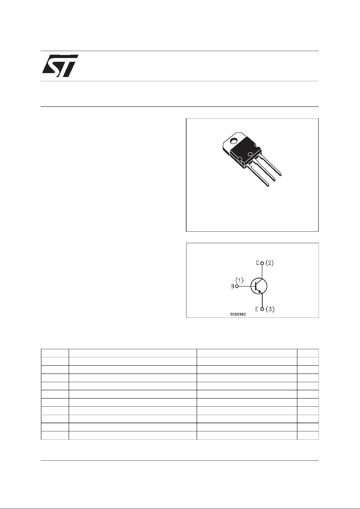
TO-218
3
2
1
The BUF420A is manufactured using High
Voltage Multi Epitaxial Planar technology for high
switching speeds and high voltage capacity. It
use a Cellular Emitter structure with planar edge
termination to enhance switching speeds while
maintaininga wide RBSOA.
INTERNAL SCHEMATIC DIAGRAM
The BUF series is designed for use in
high-frequency power supplies and motor control
applications.
ABSOLUTE MAXIMUM RATINGS
Symb o l Parame t er Val u e Uni t
V
V
V
I
I
P
T
Collector-Emitter Voltage (VBE= -1. 5V) 1000 V
CEV
Collector-Emitter Voltage (IB= 0) 450 V
CEO
Emitter-Base Voltage (IC=0) 7 V
EBO
Collect or Current 30 A
I
C
Collect or Peak Cu rr ent ( tp<5ms) 60 A
CM
Base Current 6 A
I
B
Base Peak Current (tp<5ms) 9 A
BM
Total Dissipat ion at Tc=25oC 200 W
tot
Stora ge T emper at u re -65 to 150
stg
Max. Oper at i ng Junction Tem per at u r e 150
T
j
o
C
o
C
June 2000
1/6
Page 2

BUF420A
THERMAL DATA
R
thj-case
Ther mal Resistance Junction-Case Max 0.63
o
C/W
ELECTRICAL CHARACTERISTICS (T
=25oC unless otherwisespecified)
case
Symbol Parameter Test Cond itions Min. Typ. Max. Unit
I
CER
I
CEV
I
EBO
V
CEO(sus )
Collector C ut -of f
Current (R
BE
=5Ω)
Collector C ut -of f
Current (V
= -1. 5V)
BE
Emit ter Cut -off Curr ent
=0)
(I
C
∗ Collec tor-Emit t er
V
=1000V
CE
=1000V Tc= 100oC
V
CE
V
=1000V
CE
=1000V Tc= 100oC
V
CE
V
=5V 1 mA
BE
I
= 200 m A L = 25 mH 450 V
C
0.2
1
0.2
1
Sust aining Volt age
=0)
(I
B
V
V
CE(sat)
EBO
Emit ter Bas e Vo lt age
=0)
(I
C
∗ Collector-Emit t er
Saturation Voltage
V
∗ Base-Emitt er
BE(sat)
Saturation Voltage
di
/dt Rate of rise on-state
c
Collector C urr ent
V
(3µs) Co llector-Emit t er
CE
Dynamic V o lt age
V
(5µs) Co llector-Emit t er
CE
Dynamic V o lt age
INDUCTIVE LOAD
t
t
St orage Time
s
t
Fall Time
f
Cross Over Time
c
INDUCTI VE LO A D
V
t
t
CEW
St orage Time
s
t
Fall Time
f
Cross Over Time
c
Maximum Collector
Emit ter Voltage
without Snubber
INDUCTI VE LO A D
t
t
St orage Time
s
t
Fall Time
f
Cross Over Time
c
I
=50mA 7 V
E
IC=10A IB=1A
=10A IB=1A Tc=100oC
I
C
=20A IB=2A
I
C
=20A IB=2A Tc=100oC
I
C
IC=10A IB=1A
=10A IB=1A Tc=100oC
I
C
=20A IB=2A
I
C
=20A IB=2A Tc=100oC
I
C
=300V RC=0 tp=3µs
V
CC
=1.5A Tj=25oC
I
B1
=1.5A Tj=100oC
I
B1
=6A Tj=100oC
I
B1
=300V RC=60Ω
V
CC
I
=1.5A Tj=25oC
B1
=1.5A Tj=100oC
I
B1
=300V RC=60Ω
V
CC
=1.5A Tj=25oC
I
B1
=1.5A Tj=100oC
I
B1
70
150
0.8
2.8
0.5
2
0.9
1.5
1.1
1.5
100 A /µs
2.1
8
1.1
4
IC=10A VCC=50V
=-5V RBB=0.6 Ω
V
BB
= 400 V IB1=0.5A
V
clamp
L = 0.25 mH
1
0.05
0.08
IC=10A VCC=50V
=-5V RBB=0.6Ω
V
BB
= 400 V IB1=1A
V
clamp
L = 0.25 mH T
=100oC
j
IC=10A VCC=50V
=-5V RBB=0.6Ω
V
BB
= 400 V IB1=1A
V
clamp
L = 0.25 mH T
=125oC
j
500 V
2
0.1
0.18
IC=10A VCC=50V
=0 RBB=0.15Ω
V
BB
= 400 V IB1=1A
V
clamp
L = 0.25 mH
1.5
0.04
0.07
mA
mA
mA
mA
V
V
V
V
V
V
V
V
A/µs
A/µs
V
V
V
V
µs
µs
µs
µs
µs
µs
µs
µs
µs
2/6
Page 3

BUF420A
ELECTRICAL CHARACTERISTICS (continued)
Symbol Parameter Test Cond itions Min. Typ. Max. Unit
V
V
t
s
t
f
t
c
CEW
t
s
t
f
t
c
t
s
t
f
t
c
CEW
INDUCTI VE LO A D
St orage Time
Fall Time
Cross Over Time
Maximum Collector
Emit ter Voltage
without Snubber
INDUCTI VE LO A D
St orage Time
Fall Time
Cross Over Time
INDUCTI VE LO A D
St orage Time
Fall Time
Cross Over Time
Maximum Collector
Emit ter Voltage
without Snubber
IC=10A VCC=50V
=0 RBB=0.15Ω
V
BB
= 400 V IB1=1A
V
clamp
L = 0.25 mH T
=100oC
j
IC=10A VCC=50V
=0 RBB=0.15Ω
V
BB
= 400 V IB1=1A
V
clamp
L = 0.25 mH T
=125oC
j
IC=20A VCC=50V
=-5V RBB=0.6 Ω
V
BB
= 400 V IB1=4A
V
clamp
L = 0.12 mH
IC=20A VCC=50V
=-5V RBB=0.6Ω
V
BB
= 400 V IB1=4A
V
clamp
L = 0.12 mH T
I
=30A VCC=50V
CWo f f
=-5V RBB=0.6Ω
V
BB
L = 0.08 mH I
=125oC
T
j
=125oC
j
=6A
B1
3
0.15
0.25
500 V
2.2
0.06
0.12
3.5
0.12
0.3
400 V
µs
µs
µs
µs
µs
µs
µs
µs
µs
Turn-onSwitching Test Circuit.
1) Fast electronic switc h
2) N on-inductive Resist or
Turn-offSwitching TestCircuit.
1) Fast electronic switc h
2) N on-inductive Resist or
3) Fast recovery rectif ier
3/6
Page 4

BUF420A
Turn-onSwitching Test Waveforms.
Turn-offSwitching Test Waveforms
ForwardBiased Safe Operating Areas.
(inductiveload).
ReverseBiased Safe Operating Area StorageTime Versus Pulse Time.
4/6
Page 5

TO-218 (SOT-93) MECHANICAL DATA
BUF420A
DIM.
MIN. TYP. MAX. MIN. TYP. MAX.
A 4.7 4.9 0.185 0.193
C 1.17 1.37 0.046 0.054
D 2.5 0.098
E 0.5 0.78 0.019 0.030
F 1.1 1.3 0.043 0.051
G 10.8 11.1 0.425 0.437
H 14.7 15.2 0.578 0.598
L2 – 16.2 – 0.637
L3 18 0.708
L5 3.95 4.15 0.155 0.163
L6 31 1.220
R – 12.2 – 0.480
Ø 4 4.1 0.157 0.161
mm inch
E
A
C
L5
D
L6
L3
L2
H
G
¯
F
R
123
P025A
5/6
Page 6

BUF420A
Information furnished is believed tobeaccurate and reliable. However, STMicroelectronics assumes noresponsibility for theconsequences
of use of such information nor for any infringement of patents or other rights of third parties which may result from its use. No license is
granted by implication or otherwise under any patent or patent rights of STMicroelectronics. Specification mentioned in this publication are
subject tochange without notice. This publication supersedes and replaces all information previously supplied. STMicroelectronics products
are notauthorized for use as critical components in life support devices or systems without express written approval of STMicroelectronics.
The ST logo is a trademark of STMicroelectronics
2000 STMicroelectronics – Printed in Italy – All Rights Reserved
STMicroelectronicsGROUP OF COMPANIES
Australia - Brazil - China - Finland - France - Germany - Hong Kong - India - Italy- Japan - Malaysia - Malta - Morocco -
Singapore- Spain - Sweden - Switzerland -United Kingdom - U.S.A.
http://www.st.com
6/6
 Loading...