

Page 1
1
Memory ICs
Non-volatile electronic potentiometer
BU9831 / BU9831F
The BU9831 / BU9831F is a non-volatile electronic potentiometer with an internal 2k bit EEPROM. The resistance
value can be set by means of serial communications, and because the product contains an internal memory, conditions can be retained.
In addition, the 2k bit memory capacity enables digital data to be stored in the memory.
•
Absolute maximum ratings (Ta = 25°C)
Applied voltage
Power
dissipation
BU9831
BU9831F
Pd
Storage temperature
Operating temperature
Input voltage
∗
1 Reduced by 5.0mW for each increase in Ta of 1°C over 25°C.
∗
2 Reduced by 3.5mW for each increase in Ta of 1°C over 25°C.
VCC
Parameter Symbol
Tstg
Topr
—
– 0.3 ~ + 7.0
Limits
– 65 ~ + 125
– 20 ~ + 85
– 0.3 ~ V
CC + 0.3
mW
V
Unit
°C
°C
V
Wiper current
I
W
± 1.0 mA
500
∗
1
350
∗
2
•
Applications
Portable LCD backlight adjustment devices for notebook computers, and other sound adjustment devices for sets
•
Features
1) Internal 2k bit EEPROM
2) 100kΩ (1kΩ×100 steps) electronic potentiometer
3) Data in memory is automatically read when power supply is turned on, and resistance value is set.
4) Resistance value can be set using serial communications.
5) Low current consumption
When operating: 3mA (max.)
In standby mode: 200µA (max.)
•
Recommended operating conditions
Power supply voltage
Power supply voltage for writing Vccwr
VCC
Parameter Symbol
V
V
Unit
2.7 ~ 5.5
Limits
2.8 ~ 5.5
Input voltage V
IN V 0 ~ VCC
Voltage at resistor ends VRHL V 0 ~ VCC
Wiper pin voltage VW V 0 ~ VCC
Page 2
2
Memory ICs BU9831 / BU9831F
•
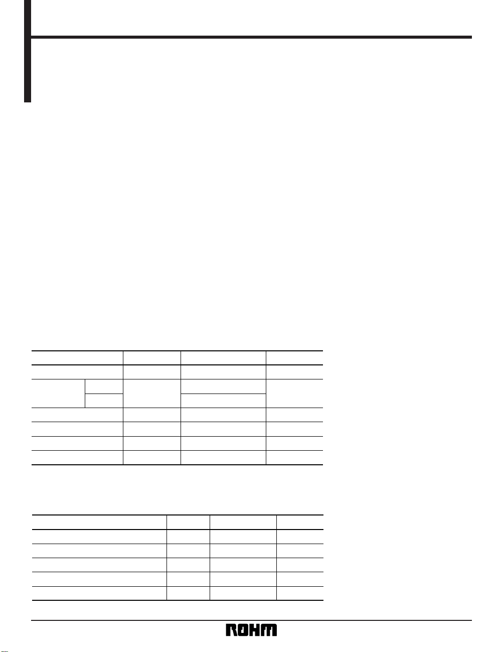
Block diagram
Command decode
Control
Timing Counter
EEPROM
Array
Wiper
decoder
Transistor
switch
Register
array
VW
VL
VH
High
voltage
generator
Write
Disable
Power supply
voltage detector
7bit
16bit
SK
DIO
CS
•
Pin assignments
CS SK DIO GND
VCC VH VW VL
BU9831
1234
8765
•
Pin desoriptions
DIO Input / output of operating codes, addresses, and serial data
GND Reference voltage of 0V for all input / output
VH Resistance high-potential
VCC Connection for power supply
I / O
—
Resistance pin
—
Pin name
3
4
7
SK Serial data clock input
VW Wiper
I
Resistance pin
2
6
CS Chip select input
VL Resistance low-potential
I
Resistance pin
1
5
8
Pin No. FunctionI / O
Page 3
3
Memory ICs BU9831 / BU9831F
•
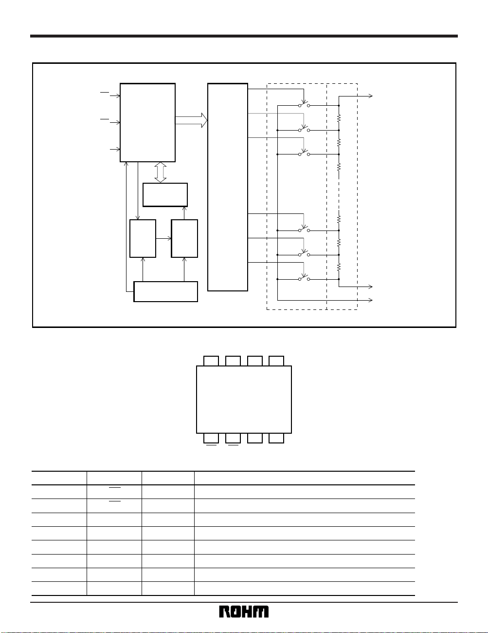
Input circuits
RESET int.
CS
SK
CS int.
•
Output circuits
CS int.
DIO
OE int.
•
Electrical characteristics (unless otherwise noted, Ta = – 20 to + 85°C, VCC = 5V ± 10%)
Input low level voltage
V
IL
Parameter Symbol Min. Typ. Max. Unit
——
0.2 ×
V
CC
V
0.8
×
V
CC
——V
0—0.4 V
VCC –
0.4
—V
CC V
– 1 — 1 µA
–1 — 1 µA
—— 3mA
——200 µA
—— 1 MHz
— 100 — kΩ
— 0.5 1 kΩ
0—VCC V
0—VCC V
Measurement
Circuit
CS, SK, DIO pin
Input high level voltage
V
IH
CS, SK, DIO pin
Output low level voltage
V
OL
IOL = 2.1mA
I
OH = – 0.4mAOutput high level voltage
V
OH
Input leakage current
I
LI
VIN = 0 ~ VCC
Output leakage current
I
LO
VOUT = 0 ~ VCC, CS = VCC
Operating current consumption
ICC
f = 1MHz, tE / W = 10ms (WRITE) Fig.5
Fig.4
Fig.3
Fig.6
Fig.1
—
—
Standby current
I
SB
CS, SK, DIO, VH, VL, VW = VCC Fig.6
SK frequency
f
SK
Total resistance
R
T
If = 10µA
Wiper resistance
R
W
IW = – 1mA Fig.8
Fig.7
—
—
Resistance potential on High side
VVH
—
Resistance potential on Low side
VVL
Conditions
Page 4
4
Memory ICs BU9831 / BU9831F
(unless otherwise noted, Ta = – 20 to + 85°C, VCC = 3V ± 10%)
Input low level voltage
VIL
Parameter Symbol Min. Typ. Max. Unit
——
0.2 ×
V
CC
V
0.8
×
V
CC
——V
0—0.4 V
VCC –
0.4
—V
CC V
– 1 — 1 µA
– 1 — 1 µA
—— 2mA
——100 µA
——500 kHz
— 100 — kΩ
— 12kΩ
0—VCC V
0—VCC V
Measurement
Circuit
CS, SK, DIO pin
Input high level voltage
VIH
CS, SK, DIO pin
Output low level voltage
VOL
IOL = 100µA
I
OH = – 100µA
Output high level voltage
VOH
Input leakage current
ILI
VIN = 0 ~ VCC
Output leakage current
ILO
VOUT = 0 ~ VCC, CS = VCC
Operating current consumption
ICC
f = 1MHz, tE / W = 10ms (WRITE) Fig.5
Fig.4
Fig.3
Fig.6
Fig.1
—
—
Standby current
I
SB
CS, SK, DIO, VH, VL, VW = VCC Fig.6
SK frequency
f
SK
Fig.7Total resistance
R
T
If = 10µA
Wiper resistance
R
W
IW = – 500µA Fig.8
Resistance potential on High side
VVH
—
Resistance potential on Low side
VVL
—
Conditions
•
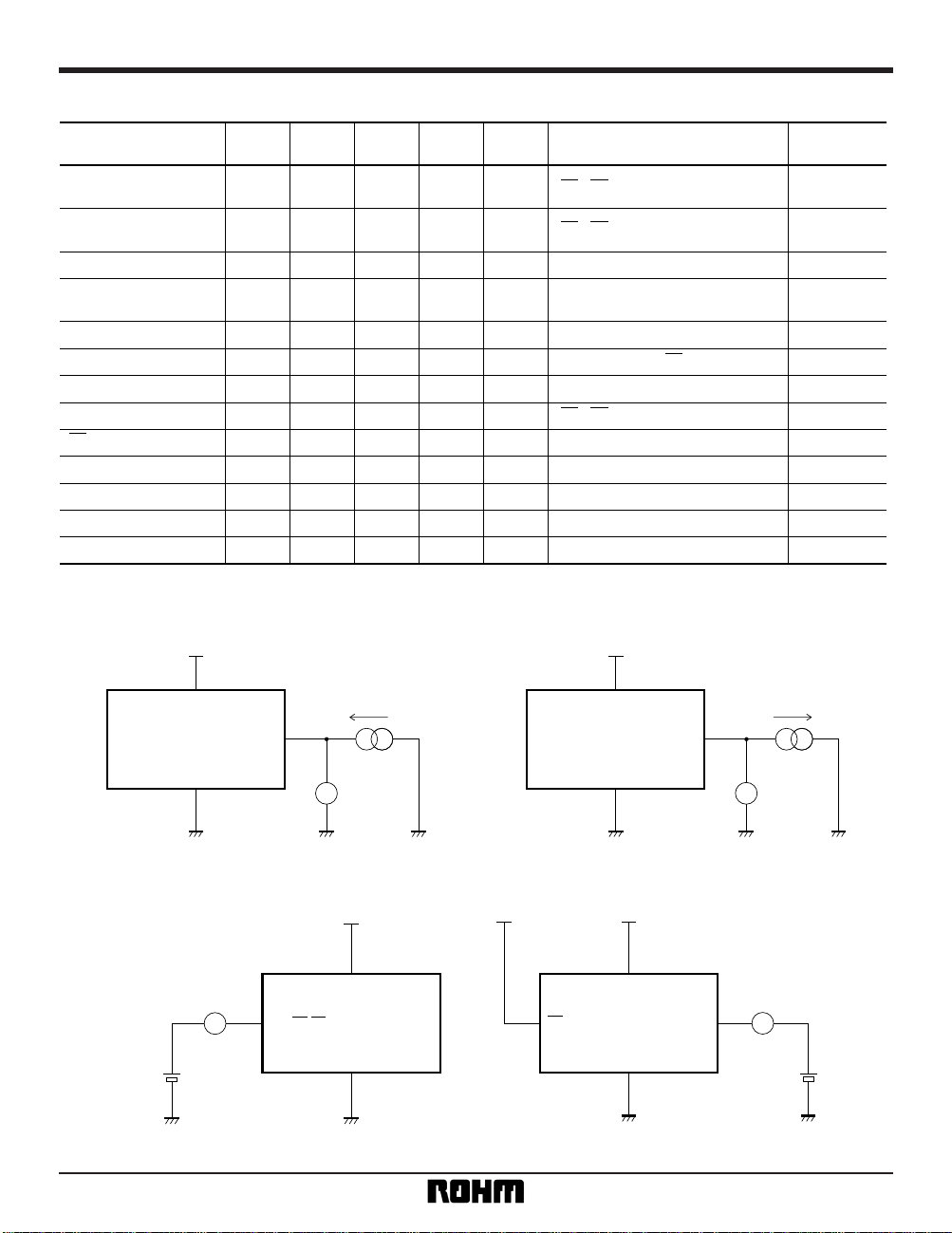
Measurement circuits
VCC
VOL
IOL
VCC
DIO
GND
Data set when output is LOW
V
Fig. 1 LOW output voltage measurement circuit
VCC
VOH
IOH
VCC
DIO
GND
Data set when output is HIGH
V
Fig. 2 HIGH output voltage measurement circuit
VCC
ILI
VCC
DIO, SK, CS
GND
A
VIN = 0 ~ VCC
Fig. 3 Input leakage current measurement circuit
VCCVCC
ILO
VO = 0 ~ VCC
VCC
CS
DIO
GND
A
Fig. 4 Output leakage current measurement circuit
Page 5

5
Memory ICs BU9831 / BU9831F
VCC
ICC
VCC
DIO
GND
A
SK
CS
Input
1MHz Clock
V
IL
Fig. 5 Current consumption measurement circuit
VCC
VCC VCC
ISB
V
CC
DIO
VH, VL, VW
GND
A
SK
CS
Fig. 6 Standby current measurement circuit
VCC
GND
V
DIO
V
W
VH
VL
I force
R
T =
V
I force
I force = 10µA
CS
SK
Fig. 7 Total resistance measurement circuit
IW
VCC
GND
V
DIO
V
W
VH
VL
V force
Measured after wiper
position is set to 64h
RWL = V / IW
V force = 1 / 2 · VCC
SK
CS
Fig. 9 Wiper resistance measurement circuit on High side
VCC
GND
V
DIO
V
W
VH
VL
IW
V force
Measured after wiper
position is set to 00h
RWL = V / IW
V force = 1 / 2 · VCC
CS
SK
Fig. 8 Wiper resistance measurement circuit on Low side
Page 6

6
Memory ICs BU9831 / BU9831F
•
Command modes
Command
Write enabled
Write disabled
Wiper counter data output
Wiper counter data input
Data read
Data write
Transmission memory data read
Transmission memory data write
Increment / decrement wiper
WEN
WDS
WCR
WCW
DRD
DWR
D8 - D14 X
XXXXXXXX D8 - D14 X
D0 - D15
D0 - D15
Wiper counter → output
Input → wiper counter
Memory → output
Input → memory
Memory → wiper counter
Wiper counter → memory
Wiper counter → INC / DEC
TDWR
TWDW
INC/DEC
Start bit
Operation code
Address
1010 0011
XXXXXXXX
1010 0000
XXXXXXXX
1010 1011
XXXXXXXX
1010 0110
XXXXXXXX
1010 1000 A0 - A6 X
1010 0100 A0 - A6 X
1010 1001 A0 - A6 X
1010 0101 A0 - A6 X
1010 1111
Data Operation
X: Don't Care (data may be either 0 or 1)
—
—
—
—
—
—
—
䊊
Auto recall function (ARF)
• After the power supply is turned on, the data for address 00h is automatically loaded and the wiper position set. At
this point, if the data for address 00h is larger than 64h, the wiper position is set to 32h. Since the wiper position is
set using seven bits, the eighth bit may be set to any value. This function is carried out 10ms after the power supply
is turned on, and subsequently the IC enters the standby state.
•
Operation timing characteristics (unless otherwise noted, Ta = – 20 to + 85°C, VCC = 5V ± 10%)
Parameter
Symbol
Min. Typ. Max. Unit
t
CSS 200 — — ns
CS setup time
t
CSH 0——ns
CS hold time
t
DIS 150 — — ns
Data setup time
t
DIH 150 — — ns
Data hold time
t
PD1 — — 350 ns
DO rise delay time
t
PD0 — — 350 ns
DO fall delay time
tE / W — — 10 ms
Self-timed programming cycle
t
CS 1——µs
CS minimum HIGH time
t
SV —— 1 µs
Time during which READY / BUSY display is effective
tOH 0 — 400 ns
Time that DO is HIGH-Z from (CS)
t
WH 450 — — ns
Data clock HIGH time
t
WL 450 — — ns
Data clock LOW time
t
AW — — 500 µs
Resistance value stabilization time
Page 7

䊊
Reading of input data is done at the rising edge of SK.
䊊
Output of data is synchronized to the falling edge of SK.
䊊
Between commands, CS should be set to HIGH for longer than tCS.
If CS remains LOW, the next command cannot be received.
7
Memory ICs BU9831 / BU9831F
(unless otherwise noted, Ta = – 20 to + 85°C, VCC = 5V ± 10%)
Parameter
Symbol
Min. Typ. Max. Unit
t
CSS 400 — — ns
CS setup time
t
CSH 0——ns
CS hold time
t
DIS 300 — — ns
Data setup time
t
DIH 300 — — ns
Data hold time
t
PD1 — — 700 ns
DO rise delay time
t
PD0 — — 700 ns
DO fall delay time
tE / W — — 15 ms
Self-timed programming cycle
t
CS 2——µs
CS minimum HIGH time
t
SV —— 2 µs
Time during which READY / BUSY display is effective
tOH 0 — 800 ns
Time that DO is HIGH-Z from (CS)
t
WH 900 — — ns
Data clock HIGH time
t
WL 900 — — ns
Data clock LOW time
t
AW — — 1000 µs
Resistance value stabilization time
•
Synchronous data I / O timing
t CSS
t CSH
t PD
t DIS
t PD
t OH
t DIH
t WH
t CS
t WL
CS
SK
Input DIO
Output DIO
Fig. 10 Synchronous data I / O timing
Page 8

8
Memory ICs BU9831 / BU9831F
•
Timing charts
(1) Writing enabled / disabled
SK
CS
DIO
H
L
H
L
H
L
ENABLE = 1 1
DISABLE = 0 0
14 8 12 16
110000
Fig. 11 Writing enabled and disabled
1) When the power supply is turned on, the writing recognition latch is reset in the same way as when the write dis-
able command is executed. The write enable command must be input before the write command is input.
2) Once the write enable command has been set, it remains effective until either the write disable command is input,
or the power supply is turned off.
3) No clocks longer than 16 clocks are required. These will be ignored by the IC if input. The command is received
following the clock input for the eight bits of the address subsequent to input of the operation code. The contents of
the address are not related to either of these commands, however, and will be ignored.
(2) Wiper counter data output (WCR)
SK
CS
DIO
1
1
1
11
000
H
L
H
L
H
L
(DO)
D8 D14
HIGH-ZHIGH-Z
14 8 16
24
t CS
Fig. 12 Wiper counter data output
1) When the Wiper Counter Data Output (WCR) command is received, seven bits of the data at the current wiper
position are output to D8, D9, D10, ..., D14, in sequential order. If a clock of longer than 24 clocks is input, indefinite
data may be output. (For the DIO output, the data may change at the tPD0 and tPD1 time delays, in response to the
internal circuit delay starting from the falling edge of the SK signal. During the tPD0 and tPD1 time internals, data
should be loaded after the tPD time has been assured, in case the previous data is indefinite. Refer to Fig. 10,
Synchronous data I / O timing.)
Page 9

9
Memory ICs BU9831 / BU9831F
(3) Wiper counter data input (WCW)
SK
CS
DIO
1
1
0
10
001
H
L
H
L
H
L
VW
14 8
24 32
t AW
D8 D14
Fig. 13 Wiper counter data input
1) This command is used for direct input of wiper position data. Since the data is 7-bit data sequentially input in the
order of D8, D9, D10, ..., D14, it determines one wiper position among 100 taps. Since no address exists at this
point, the address is ignored. The resistance stabilizes after an interval of tAW from the rise of the 32nd clock.
(4) Data read (DRD)
SK
CS
DIO
1
1
1
0A0 A60
00 0
H
L
H
L
H
L
(DO)
D0 D15
HIGH-ZHIGH-Z
14 8 16
32
t CS
Fig. 14 Data read
1) When the data read (DRD) command is received, data is output from the addresses specified by A1 and A0.
2) Output is synchronized to the fall of SK, in order of D0, D1, D2, ..., D15, at the fall of the 16th clock. After 32
clocks have elapsed, the D15 data is retained even if other clocks are input.
Page 10

10
Memory ICs BU9831 / BU9831F
(5) Data write (DWR)
SK
CS
DIO
110 00001
H
L
H
L
H
L
14 8
16 32
t E / W
A0 A6 D0 D15
Fig. 15 Data write
1) This command stores the input data in the address specified by A0 to A6.
2) CS must be LOW during the write mode input, but once writing begins, CS may be either HIGH or LOW.
3) The internal timer circuit in the IC begins to function after the rising edge of the SK at which the last data D0 was
read, and data is written to memory cells during the time period tE / W. The process is terminated automatically.
At this point, the SK input during the tE / W time period may be either HIGH or LOW.
4) The time period between input of this command and the automatic termination of the writing of data is the time
during which data is written to the internal non-volatile memory, so commands input during this interval will not be
accepted. The maximum time interval must be within tE / W.
5) After the write command has been input, if CS is set to LOW after having been set to HIGH, command reception
is enabled following termination of the automatic data writing. Data can then be received from SK and DIO. If CS is
left at LOW following input of the command, however, without being set to HIGH, input of the command is canceled.
(6) Transmission memory data read (TDWR)
SK
CS
DIO
0
1 1 1 1 A0 A60000
H
L
H
L
H
L
VW
14 8 16
t AW
Fig. 16 Transmission memory data read
1) This command transmits the data from the addresses specified by A0 to A6 to the wiper counter. The wiper
moves to the position indicated by the seven bits D8 to D14 of the specified address, and the resistance value stabilizes after the tAW time period starting with the fall of the 15th clock. Data subsequent to the 16th clock is ignored.
Page 11

11
Memory ICs BU9831 / BU9831F
(7) Transmission memory data write (TWDW)
SK
CS
DIO
1
1
1
1A0 A60
000
H
L
H
L
H
L
14 8 16
t E / W
Fig. 17 Transmission memory data write
1) This command transmits the wiper position data to the addresses specified by A0 to A6. The data from the seven
bits D8 to D14 of the specified address are stored in the memory during the time tE / W, starting from the rise of the
16th clock.
2) Writing is done to the internal non-volatile memory during the time when this command is input and automatic
writing of the data is completed. Commands input during this time will not be accepted. The maximum time for this
period must be within tE / W.
3) After the write command has been input, if CS is set to LOW after having been set to HIGH, command reception
is enabled following termination of the automatic data writing. Data can then be received from SK and DIO. If CS is
left at LOW following input of the command, however, without being set to HIGH, input of the command is canceled.
(8) INC / DEC
SK
CS
DIO
1 1 1 1 DEC INC1001
H
L
H
L
H
L
VW
1 4 8 9 10 11
t AW
t AW t AW
Fig. 18 Increment / decrement wiper
1) The wiper position is incremented or decremented starting from the next clock following input of the INC / DEC
command, based on the status of the INC pin.
DIO = H: Incremented. The wiper position moves from the VL to the VH side by 1 tap per clock.
DIO = L: Decremented. The wiper position moves from the VH to the VL side by 1 tap per clock.
2) The tap is moved at each rise of the clock, until CS is set to HIGH.
When the tap is farthest to the VH side, incrementing is ignored.
In the same way, when the tap is farthest to the VL side, decrementing is ignored.
Page 12

12
Memory ICs BU9831 / BU9831F
•
Application examples
BU9831
VH
VW
VL
Fig. 19 Operation amplifier gain adjustment
BU9831
Fine adjustment of the input offset voltage can be done in order to
suppress the error voltage of the output based on the input voltage.
Fig. 20 Adjustment of the operation amplifier offset voltage
Reg
Output current can be adjusted by adjusting the output load.
BU9831
Fig. 21 Variable output adjustment of regulator
•
Operation notes
(1) When turning the power supply on and off
1) When turning the power supply on and off, CS should be set to HIGH ( = V
CC).
2) When CS is LOW, the BU9831 is active, meaning that input can be received. If the power supply is turned on in
this state, noise and other factors can cause malfunctioning and erroneous writing. To prevent this, when turning the
power supply on, make sure that CS is HIGH ( = V
CC).
(Example of proper operation) The CS pin is pulled up to V
CC.
After turning the power supply off, wait at least 10ms before turning it on again.
If the power supply is turned on without observing this condition, please be aware that there may be times
when the circuits in the IC are not reset.
(Example of incorrect operation) The CS pin is LOW when the power supply is turned on or off.
In this case, CS is normally LOW, and the EEPROM may cause malfunctioning or erroneous writing
because of noise.
∗ Be aware that the case shown in this example may occur even if the CS input is HIGH-Z.
Page 13

13
Memory ICs BU9831 / BU9831F
VCC
VCC
GND
VCC
CS
GND
Correct example
Incorrect example
(2) Noise countermeasures
1) SK noise
If there is noise in the rise of the SK clock input, the system may recognize more clocks than were actually input,
and malfunctioning may occur because of offset bits.
2) V
CC noise
Noise and surges in the power supply line can cause malfunctioning. To eliminate these factors, we recommend
installing a bypass capacitor between the power supply and the ground.
•
External dimension (Units: mm)
DIP8 SOP8
BU9831 BU9831F
0.5 ± 0.1
3.2 ± 0.2 3.4 ± 0.3
85
14
9.3
± 0.3
6.5 ± 0.3
0.3
±
0.1
0.51Min.
2.54
0° ~ 15°
7.62
0.4 ± 0.11.27
0.15
0.3Min.
0.15 ± 0.1
0.11
6.2 ± 0.3
4.4 ± 0.2
5.0 ± 0.2
85
41
1.5 ± 0.1
 Loading...