

Page 1
BU9817FV
Multimedia ICs
4-channel temperature sensor IC for
2
PCs with I
BU9817FV
The BU9817FV is a 4-channel, 8-bit, A / D converter / overvoltage detector that is perfect for temperature sensors with
2
built-in I
!
Notebook computers, desktop computers, household
electric appliances
!
1) By attaching a thermistor, a maximum four-channel
temperature sensor is possible.
2) Can set comparison voltages independently.
3) Built-in I
4) Detection level and operating mode settings are pro grammable.
C BUS interfaces. The host can access the BU9817FV anytime for the voltage data.
Applications
Features
2
C BUS interface.
C BUS interface
5) Extremely low operating current perfect for portable
equipment.
6) Operating voltage of V
DD
= 3V to 5.5V.
Absolute maximum ratings
!!!!
Parameter Symbol Limits Unit
Power supply voltage
Power dissipation
Operating temperature
Storage temperature
Voltage applied to pins
* Reduced by 3.5mW for each increase in Ta of 1˚C over 25˚C.
Recommended operating conditions
!!!!
Parameter Symbol UnitMax.Typ.Min.
Operating power supply voltage
(Ta = 25°C)
V
DD
Pd
Topr
Tstg
V
IN
V
DD
7.0
350
– 15 ~ + 75
– 55 ~ +125
GND – 0.5 ~ V
DD
(Ta = 25°C)
3.0 5.5— V
+ 0.5
V
mW
˚C
˚C
V
Note) I2C BUS is a registered trademark philips.
Page 2
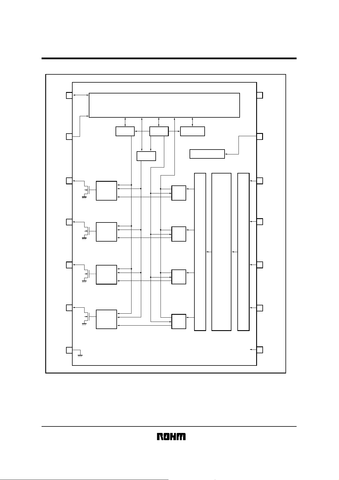
Multimedia ICs
Block diagram
!!!!
BU9817FV
SDA
SCL
OD1
OD2
Sel
14 VDD
13 STOPB
12
AD1
11
AD2
1
I2C BUS Interface
Vul
Register
Pointer
Register
Vdl
2
3
4
Reset
Voltage
Hysteresis
Comparator
Reset
Voltage
Hysteresis
Comparator
Register
ADV
Register
ADV
Register
Configuration
Register
Reset & Shutdown
Sel
Reset
Shutdown
8bit
A / D
OD3
OD4
GND
AD3
5
6
7
Reset
Voltage
Hysteresis
Comparator
Reset
Voltage
Hysteresis
Comparator
ADV
Register
ADV
Register
10
AD4
9
CLK
8
Page 3

Multimedia ICs
Pin descriptions
!!!!
Pin No. Pin name Function
10
11
12
13
14
1
2
3
4
5
6
7
8
9
SDA
SCL
OD1
OD2
OD3
OD4
GND
CLK
AD4
AD3
AD2
AD1
STOPB
DD
V
I2C BUS Serial Data Line
2
C BUS Serial Clock Input
I
Open Drain Output 1
Open Drain Output 2
Open Drain Output 3
Open Drain Output 4
Ground
Clock for Logic Input
Analog-to-Digtal Converter Input 4
Analog-to-Digtal Converter Input 3
Analog-to-Digtal Converter Input 2
Analog-to-Digtal Converter Input 1
Reset & Power save mode set
Supply Voltage 3.0V to 5.5V
BU9817FV
Page 4

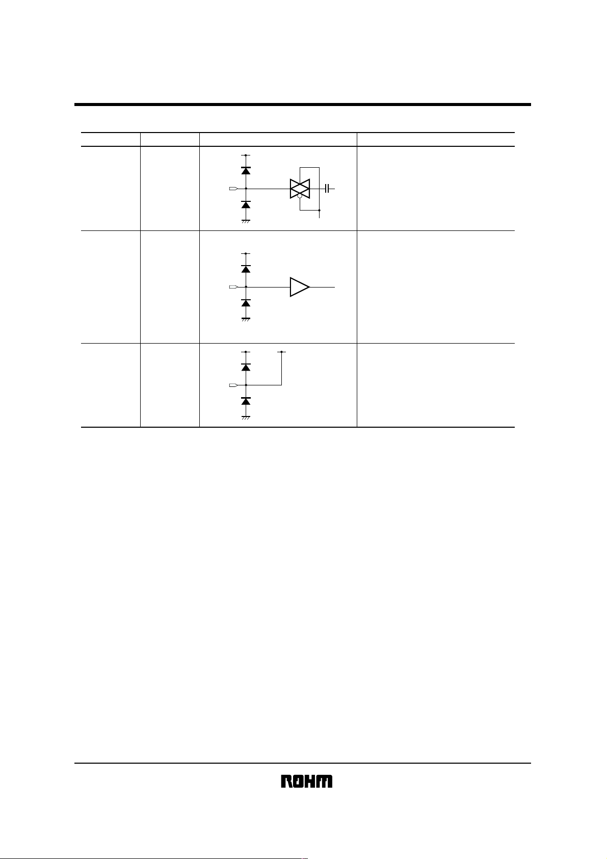
Multimedia ICs
Input / output equivalent circuits
!!!!
Pin. No Pin name Input / output circuits Function
2
I
C BUS serial data input / output.
1
2
SDA
SCL
When only input address accords slave
address (BU9817FV's), register data is
inputted or outputted.
2
I
C BUS serial clock input.
BU9817FV
3
4
5
6
7
8
OD1
OD2
OD3
OD4
GND
CLK
Open-drain output corresponds to AD1 to
AD4 input.
Connect this pin a pull-up resister.
The pull-up resister should be above V
4mA (Ω).
Ground terminal.
Clock input for ADC block.
Input clock is 32.768kHz.
AD converter and voltage hysteresis
comparator use this clock to operate.
DD
/
Page 5
Multimedia ICs
Input / output equivalent circuits
!!!!
Pin. No Pin name Input / output circuits Function
BU9817FV
10
11
12
13
14
9
AD1
AD2
AD3
AD4
STOPB
V
DD
AD input.
Each channel is converted in order.
(AD1, AD2, AD3, AD4, AD1,AD2...)
Reset and power save mode setting.
High: Operation mode
Operation follows the setting of
configuration register.
Low : Reset & Power save mode
Reset the all internal circuit and stop
the ADC operation.
Go into power save mode.
∗
Be sure to set STOPB pin low for initial
reset of the internal circuit, when the
BU9816FV is power up.
Power supply.
Supply voltage 3.0V to 5.5V.
Page 6

Multimedia ICs
Electrical characteristics
!
BU9817FV
(unless otherwise noted, VDD = 5.0V, Ta = 25°C)
Parameter
Circuit current (normal)
Circuit current
(shutdown / reset / STOPB)
Input high level voltage
Input low level voltage
Input high level current
Input low level current
Input capacity
Open drain output
low level voltage
SDA
output low level voltage
SDA
output fall time
STOPB
minimum pulse width
〈STOPB minimum pulse width〉
V
DD
GND
Minimum pulse width
Symbol Min. Typ. Max. Unit Conditions
I
CC
0.2
0.75
2.0
mA
SDA, SCL = “H”
CLK = 32.768kHz
SDA, SCL = “H”
ICC.sd
—
1.0
2.0
CLK = 32.768kHz
µA
Mode setting or
STOPB = Low
—
V
—
V
—
µA
—
µA
—
pF
V
loL = 4.0mA
loL = 6.0mA
V
CL = 400pF
ns
loL = 6.0mA
µs
—
0.3V
iH
V
V
iL
I
iH
I
iL
Ci
VoLod
VoLsda
tfsda
pwstopb
DD
DD
V
– 0.5
—
– 1.0
—
0.0
0.0
—
10
× 0.7
V
0.0
0.0
0.0
—
0.2
0.2
—
—
DD
DD
+ 0.5
V
V
DD
× 0.3
1.0
—
10
0.6
0.6
250
—
〈A / D〉
AD resolution
Non-linearity error
Differential non-linearity error
1-channel conversion time
Input range
RES
Nle
Ndle
Tc
Ai
—
– 2
– 1
—
GND
—
—
305
—
8
—
—
V
bits
2
LSB
1
DD
LSB
µs
V
2 points connected
fCLK = 32.768kHz
—
—
—
Page 7

Multimedia ICs
Measurement circuit
!
I2C BUS
Controller
BU9817FV
A
1
V
820Ω
V
820Ω
820Ω
A
2
820Ω
14
13
AA
V
1.2kΩ
V
1.2kΩ
V
1.2kΩ
V
1.2kΩ
3
4
5
6
7
12
11
10
9
8
NNNN
32.768kHz
A
Fig.1
Page 8

Multimedia ICs
Circuit operation
!
Explanation of operating mode
Operating mode
Normal mode
Interval High mode
Interval Low mode
Shutdown mode
Configuration
register settings
00000
00110
00100
00000
∗∗
∗∗
∗∗
∗∗
0b
0b
0b
1b
ADC operation
conversion interval
1.221ms
1 second intervals
4 second intervals
Stopped
Open drain
operation timing
10th clock after
A / D conversion
10th clock after
A / D conversion
10th clock after
A / D conversion
Hold status
Register status
Normal operation
Normal operation
Normal operation
Hold data
BU9817FV
Current
consumption (typ.)
0.75mA
Note: average
less than 3µA
Note: average
less than 2µA
Less than 1µA
Reset mode
The asterisk can be either 0 or 1.
Conversion time is for fCLK = 32.768kHz.
∗
These mode setting bits (bit 0 and bits 3 to 5) are common for each channel, the last setting of bits (bit0 and bits3 to 5) is
∗
effective for all channels. Furthermore, bits 1 and 2 are independent and can be set for each channel.
Note: These parameters are reference values derived through calculations and are not guaranteed characteristic values.
∗
00
∗∗1∗∗∗
b
Stopped
Reset fixed at high
Data reset
Less than 1µA
Explanation of ADC / open drain operation
(Normal mode)
Tad = 1.221ms, 40 clock
10 clock
ADC operation
(Interval mode)
ADC operation
4ch 1ch 2ch 3ch 4ch 1ch 2ch 3ch 4ch 1ch
OD1
OD2
OD3
OD4
Tin = 1s, 4s
Tc = 1.831ms, 60 clock
10 clock 10 clock 10 clock
1ch 2ch 3ch 1ch 2ch 3ch4ch 1ch
OD1
OD2
OD3
OD4
Page 9

BU9817FV
Multimedia ICs
Circuit operation
!
Explanation of I
• Slave address
1001111R / W
MSB LSB
• Conforms to I
SCL clock frequency
Start condition hold time
Start condition setup time
Data setup time
Data hold time
Stop condition setup time
(Start conditions)
2
C BUS interface
2
C BUS standards
Parameter Symbol Min. Max. Unit
0
f SCL
t HD: STA
t SU: STA
t SU: DAT
t HD: DAT
t SU: STO
0.6
0.6
100
0.6
400
—
—
—
0
0.9
—
kHz
µs
µs
ns
µs
µs
(Data conditions)
(Stop conditions)
SCL
SDA
SCL
SDA
SCL
SDA
t SU: STA
t SU: DAT t HD: DAT
t HD: STA
t SU: STO
Page 10

Multimedia ICs
Circuit operation
!
OD output voltage response diagram
(Example: open-drain output is set active low)
Vul
Vdl
OD Output
(Comparator Mode)
BU9817FV
AD pin voltage waveform
OD Output
(Interrupt Mode)
∗∗∗
Read Read Read
Time
* Note: Resetting OD output under interrupt mode occurs at only shutdown mode or reset mode or STOPB or when data
read generated from host. Except for these cases, OD output is kept setting.
Page 11

Multimedia ICs
Circuit operation
!
Register structure
SDA
SCL
I2C BUS
Interface
Pointer
Register
(Register select)
BU9817FV
1ch Configuration Register
1ch Vdl Register
1ch Vul Register
1ch ADV Register
2ch Configuration Register
2ch Vdl Register
2ch Vul Register
2ch ADV Register
3ch Configuration Register
3ch Vdl Register
3ch Vul Register
3ch ADV Register
I2C Bus data structure
(1) Write Mode
S Address
(2) Read Mode
1) Pointer register set
S Address
2) Preset pointer register
S Address
—
AAPointer reg. Byte Write Data Byte A P
W
—
AAPointer reg. Byte
W
Sr Address ARPRead Data Byte
ARPRead Data Byte
—
A
4ch Configuration Register
4ch Vdl Register
4ch Vul Register
4ch ADV Register
—
A
S: Start condition
P: Stop condition
Sr: Restart condition
A: acknowledge
—
A: acknowledge bar
Page 12

Multimedia ICs
Mode settings table 1 / 2
(1) Pointer register (selects which registers will be read from or written to)
BU9817FV
D7 D6
00D50
D4 to D7: These bits are used for test mode and must be kept zero for normal operation.
Channel Select
D3 D2 Channel
0
0
1
1
Register Select
D1 D0 Register
0
0
1
1
D4
0
Channel 1
0
Channel 2
1
Channel 3
0
Channel 4
1
ADV Register (Read only) (Power on Reset default)
0
Configuration Register (Read / Write)
1
Vdl Register (Read / Write)
0
Vul Register (Read / Write)
1
D3
Channel Select
D2 D1
Register Select
D0
(2) ADV Register (Read only)
Channel D7 D6 D5 D4 D3 D2 D1 D0
1 ch
2 ch
3 ch
4 ch
D0 to D7: Voltage data
The defaults for the power-on-reset and reset modes are 1 for all bits.
MSB
MSB
MSB
MSB
bit6
bit6
bit6
bit6
bit5
bit5
bit5
bit5
bit4
bit4
bit4
bit4
bit3
bit3
bit3
bit3
bit2
bit2
bit2
bit2
bit1
bit1
bit1
bit1
LSB
LSB
LSB
LSB
(3) Configuration Register (Read / Write)
Channel D7 D6 D5 D4 D3 D2 D1 D0
1 ch
2 ch
3 ch
4 ch
The defaults for the power-on-reset and reset modes are 0 for all bits.
0
0
0
0
Interval
0
0
Mode
0
0
Interval
Speed
Reset Shutdown
Opendrain
Polarity
Opendrain
Polarity
Opendrain
Polarity
Opendrain
Polarity
Comp. / Int.
Comp. / Int.
Comp. / Int.
Comp. / Int.
Page 13

BU9817FV
Multimedia ICs
Mode settings table 2 / 2
D0 : Shutdown
“0” - Operation mode.
“1” - The BU9817FV stops A / D operation and goes into low power shutdown mode.
D0 bit of each channel is common bit.
D1 : Comparator / Interrupt mode
“0” - Comparator mode.
“1” - Interrupt mode.
D2 : Open Drain Polarity
“0” - active low.
“1” - active high.
D3 : Reset
“0” - Operation mode.
“1” - Reset any bits except D3 bit of the configuration register, any registers, the A / D converter, and the
voltage hysteresis comparator.
D3 bit of each channel is common bit.
D4 : Interval Speed
Set the conversion cycle time of the 8bit A / D and the voltage hysteresis comparator when D5 bit (Interval
Mode) is “1”.
“0” - conversion cycle time is 4s.
“1” - conversion cycle time is 1s.
D4 bit of each channel is common bit.
D5 : Interval Mode
“0” - normal mode.
“1” - Interval mode.
D5 bit of each channel is common bit.
(4) Vul and Vdl Register (Read / Write)
Channel D7 D6 D5 D4 D3 D2 D1 D0
1 ch
2 ch
3 ch
4 ch
D0 to D7: Voltage limit data of Vul and Vdl.
Default after power on reset and reset mode is Vul = 80h, Vdl = 66h.
MSB
MSB
MSB
MSB
bit6
bit6
bit6
bit6
bit5
bit5
bit5
bit5
bit4
bit4
bit4
bit4
bit3
bit3
bit3
bit3
bit2
bit2
bit2
bit2
bit1
bit1
bit1
bit1
LSB
LSB
LSB
LSB
Page 14

Multimedia ICs
Application example
!!!!
BU9817FV
DD
V
From system
controller
OD1 Output
OD2 Output
OD3 Output
SDA
SCL
1
2
3
4
5
14
13
12
11
10
STOPB Input (From Reset IC)
Power on Reset
V
DD
RS
AD1 Input
DD
V
RS
AD2 Input
AD3 Input
Thermal Zone
RTH
Thermal Zone
RTH
RTH: NTC Thermistor
OD4 Output
6
78
9
AD4 Input
CLK Input (fCLK = 32.768kHz)
Fig.2
Page 15

BU9817FV
Multimedia ICs
Explanation for external components
!!!!
(1) AD input pin (example when used as a temperature sensor)
To the AD input pin, input a voltage with divided resistance from a resistor and NTC thermistor. For the sensor to
measure the temperature, the NTC thermistor is used. The thermistor is a p-type semiconductor and as the temperature
increases, the resistance value becomes lower. In other words, the resistance temperature coefficient is negative,
and so the AD input pin voltage temperature characteristics are also negative.
Put nearby BU9817FV
V
CC
ADx
GND is required common and stability.
External dimensions
!!!!
5.0 ± 0.2
14
4.4 ± 0.2
6.4 ± 0.3
1
0.1
1.15 ± 0.1
0.65
BU9817FV
(Units : mm)
8
7
0.22 ± 0.1
NTC thermistor
Put nearby measured object
0.15 ± 0.1
0.3Min.
0.1
SSOP-B14
 Loading...