

Page 1

1
Standard ICs
Pulse driver for LCD drive
BU9764FV
1) Six internal level converter channels.
2) TTL input.
3) Shifts levels to convert 5V signals into 16V signals.
4) Compact SSOP-B16 package.
•
Absolute maximum ratings (Ta = 25°C)
Parameter
V
DD1
VDD2
VIN
VOUT
– 0.5 ~ VSS + 7.0
– 0.5 ~ V
SS + 20.0
– 0.5 ~ V
DD1 + 0.5
– 0.5 ~ V
DD2 + 0.5
V
Symbol Limits Unit
V
V
V
V
DD1
Pin
V
DD2
VIN1 ~ VIN6
VOUT1 ~ VOUT6
IOUT ± 10 VOUT1 ~ VOUT6mA
Topr – 25 ~ + 85 °C
Tstg – 65 ~ + 150 °C
Pd 400 mW
—
—
—
Power supply voltage (1)
Power supply voltage (2)
∗
1
Input voltage
Output voltage
Output current
Operating temperature range
Storage temperature range
Power dissipation
∗
2
∗
1 VDD2 > VDD1
∗
2 Power dissipation is reduced by – 4.0mW for each increase in Ta of 1°C over 25°C.
•
Recommended operating conditions (Ta = 25°C)
Parameter
Power supply voltage (1)
Power supply voltage (2)
Ambient temperature
V
DD1
VDD2
Ta
5.0 ± 0.5
16 ± 0.5
0 ~ 70
V
Symbol Limits Unit
V
°C
V
DD1
Pin
V
DD2
—
The BU9764FV is a level converter IC designed for LCD drive, which receives 5V signals and converts them to 16V
signals. The compact SSOP-B16 package contains six internal level converters.
•
Applications
Small- to medium-sized TFT liquid crystal panels for movie projectors, LCD projectors, and other similar devices
•
Features
Page 2

2
Standard ICs BU9764FV
•
Block diagram
1
2
3
4
5
6
7
8
VDD2
VOUT1
VOUT2
VOUT3
VSS
VOUT4
VOUT5
VOUT6
16
15
14
13
12
11
10
9
VDD1
VIN1
VIN2
VIN3
VSS
VIN4
VIN5
VIN6
•
Pin descriptions
Pin No. I / O
16
V
DD1 —
—
I
V
DD2
1
—
—
—
—
V
SS
5, 12
V
IN1 ~ VIN6
9, 10, 11
13, 14, 15
O
V
OUT1 ~ VOUT6
2, 3, 4
6, 7, 8
Pin name Function Processing when not used
Power supply pin for input buffer
Power supply pin for output buffer
Pulse input pin
Ground pin
∗
3
Pulse output pin Open
∗
3 When using the IC, ground both pins 5 and 12.
short VSS
Page 3
3
Standard ICs BU9764FV
VDD1
GND
Input pad
VDD2
VDD2
GND
Output pad
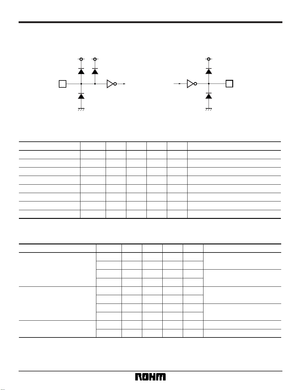
•
Input / output circuits
(1) Input circuit
Pin nos. 9, 10, 11, 13, 14, 15
(2) Output circuit
Pin nos. 2, 3, 4, 6, 7, 8
•
Electrical characteristics (unless otherwise noted, Ta = 25°C, VDD1 = 5V, VDD2 = 16V)
Parameter
V
IH
VIL
IIN
VOH
VOL
IOH
IOL 1.0
V
Symbol
2.0
—
– 1.0
15.9
—
—
Min.
—
—
—
—
16.0
0.0
—
Typ.
—
—
0.8
1.0
—
0.1
– 1.0
mA
V
mA
Max. Unit Conditions
V
µA
—
—
V
VOL = 0.5V
IDD ——20µAVIN = 0V, or VDD1
IOH = 20µA
V
OH = 15.5V
I
OH = – 20µA
Input high level voltage
Input low level voltage
Input current
Output high level voltage
Output low level voltage
Output high level current
Output low level current
Standby current
—
•
AC characteristics (unless otherwise noted, Ta = 25°C, VDD1 = 5V, VDD2 = 16V)
Parameter
t
TLH
tTHL
tTLH
tTHL
tPLH
tPHL
tPLH —
ns
Symbol
—
—
—
—
—
—
Min.
30
20
20
30
30
20
20
Typ.
60
40
40
60
60
40
40
ns
ns
ns
Max. Unit Conditions
ns
ns
ns
tPHL —3060ns
∆T——10ns
∆T——10ns
∗
4 NOT 100% TESTED
Output transition time
∗
4
Propagation delay time
Propagation delay time differential
between channels
∗
4
Load: 35pF
Load: 5pF
Load: 35pF
Load: 5pF
Load: 35pF
Load: 5pF
Page 4

4
Standard ICs BU9764FV
•
External dimensions (Units: mm)
SSOP-B16
9
8
16
1
0.1
6.4 ± 0.3
4.4 ± 0.2
5.0 ± 0.2
0.1
0.15 ± 0.1
0.22 ± 0.1
0.65
1.15 ± 0.1
0.3Min.
 Loading...