

Page 1
1
Standard ICs
Quad 2-input / 2-output analog switch
BU9761FS
The BU9761FS are analog switches with four circuits each, two for input and two for output. Depending on the status
of the SELECT pin, the two input signals can be switched to either of two output pins. In addition, the EN pin can be
used to set the output status to high impedance.
•
Applications
Videos, movies, TVs, mini-component sets, radio cassette players, audio equipment, personal computers
•
Features
1) Ultra-compact slim package. (SSOP-A20)
2) Low current dissipation. (I
Q = 1µA Max.)
3) Equipped with Output Enable terminal.
4) Low switching ON resistance. (R
ON = 130Ω)
5) Low dispersion in switching ON resistance for the
various channels. (∆RON = 25Ω Max.)
•
Absolute maximum ratings (Ta = 25°C)
Parameter Symbol Limits Unit
V
DD
V
Pd
600
∗
1
mW
Topr °C
Tstg °C
– 25 ~ + 75
– 0.3 ~ + 7.0
– 50 ~ + 150
Power supply voltage
Power dissipation
Operating temperature
Storage temperature
∗
1 Reduced by 4.8mW for each increase in Ta of 1°C over 25°C.
•
Recommended operating conditions (Ta = 25°C)
Parameter Symbol Min. Typ. Max. Unit
Power supply voltage V
DD 4.0 5.0 6.0 V
Page 2
2
Standard ICs BU9761FS
EN H L
OUT1 ~ 8 High-Z Output Enable
•
Pin truth table
• EN
• SELECT
HL
INA OB INA OA
INB OA INB OB
Input
Output
Input
Output
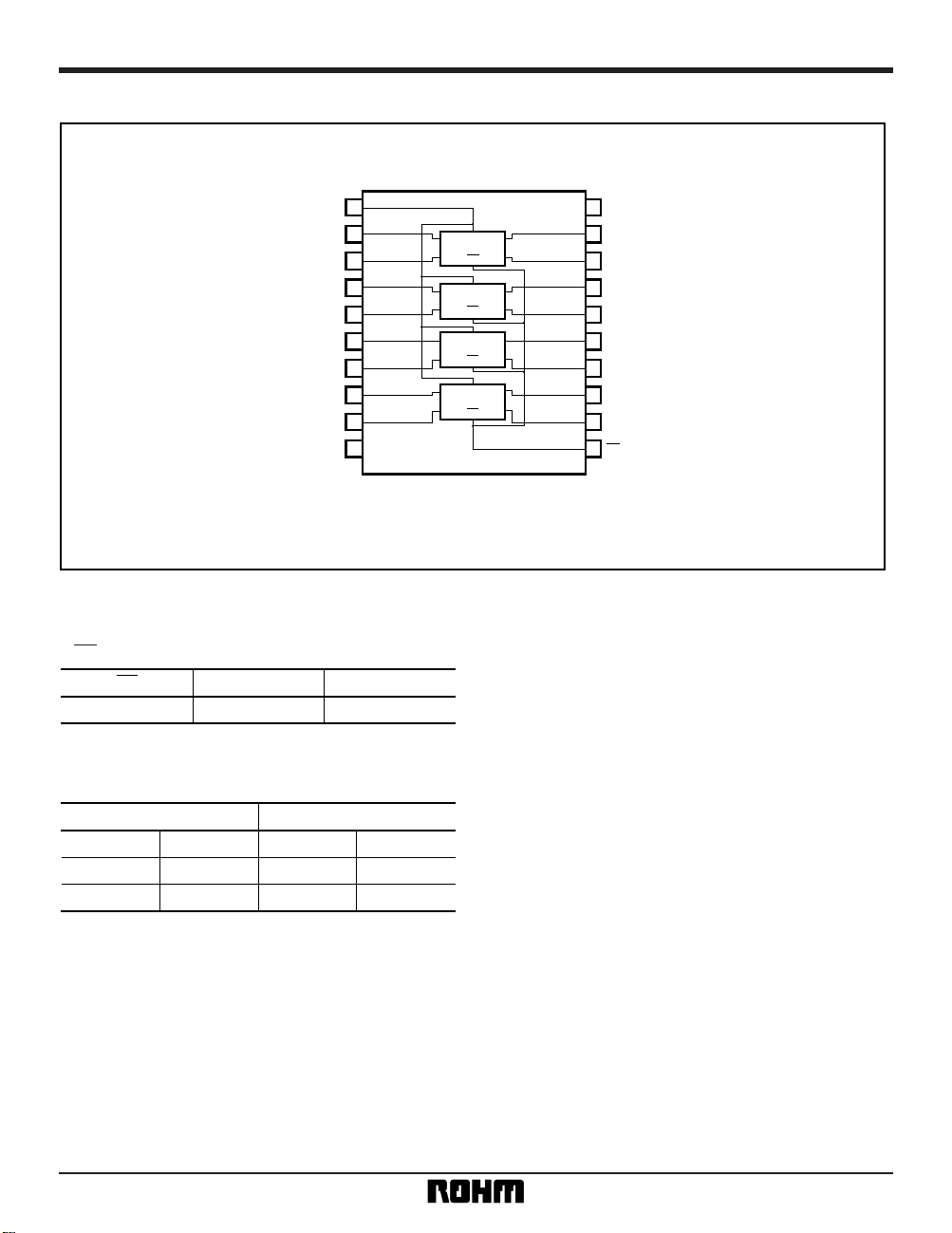
•
Block diagram
1
20
2
19
3
18
4
17
5
16
6
15
7
14
8
13
9
12
10
11
OA
OB
INA
SWA
EN
INB
OA
OB
INA
SWB
EN
INB
OA
OB
INA
SWC
EN
INB
OA
OB
INA
SWD
EN
INB
SELECT
IN1
IN2
IN3
IN4
IN5
IN6
IN7
IN8
GND
V
DD
OUT1
OUT2
OUT3
OUT4
OUT5
OUT6
OUT7
OUT8
EN
(Top View)
Page 3

3
Standard ICs BU9761FS
•
AC characteristics (unless otherwise noted, Ta = 25°C, VDD = 5V, CL = 50 pF, RL = 10kΩ)
Symbol Min. Typ. Max. Unit Conditions
Measurement
circuit
V
DD
(V)
t
PLH1
—
40
—
ns 5
Output "L"→Output "H"
Output "H"→Output "L"
Fig.4
t
PHL1
—
40
—
ns 5
t
PLH2
—
50
—
ns 5
Output "L"→Output "H"
Output "H"→Output "L"
Fig.5
t
PHL2
—
40
—
ns 5
t
PHZ
—
200
—
ns 5
Output "H"→Output "High Z"
Output "L"→Output "High Z"
Fig.6
Fig.7
t
PLZ
—
200
—
ns 5
t
PZH
—
50
—
ns 5
Output "High Z"→Output "H"
Output "High Z"→Output "L"
Fig.6
Fig.7
t
PZL
—
50
—
ns 5
C
C
—
35
—
pF 5 f = 1MHz
—
C
S
—
65
—
pF 5 f = 1MHz
—
D
—
0.06
—
% 5 Fig.8
—
1.15
—
MHz 5 V
IN
= 2.5V
P-P
Fig.8
FT
—
– 70
—
dB 5 Fig.9
CT
C
—
620
—
mV
P-P
5f = 10kHz Fig.10
CT
—
– 50
—
dB 5 Fig.11
Parameter
V
IN
= 2.5V
P-P
, f = 1kHz
V
IN
= 2.5V
P-P
, f = 10kHz
V
IN
= 2.5V
P-P
, f = 10kHz
f
Max.
Propagation delay time
IN to OUT
Propagation delay time
SELECT to OUT
Output Enable time
Output Disable time
Input capacitance
(control input)
Input capacitance
(switch input)
Sine wave distortion
(T.H.D.)
Max. propagation frequency
Feedthrough attenuation
Crosstalk
(control / switch)
Crosstalk between channels
•
DC characteristics (unless otherwise noted, Ta = 25°C, VDD = 5 V)
Parameter Symbol Min. Typ. Max. Unit Conditions
V
IH 3.5 ——VRL = 10kΩ
Fig.1
V
IL —— 1.5 V RL = 10kΩ
Fig.1
I
IH —— 0.3 µ
AR
L = 10kΩ
Fig.1
I
IL —— 0.3 µ
AR
L = 10kΩ
Fig.1
R
ON — 135 150 Ω
Fig.2
— 12 25
Ω
Fig.2
——
µ
A Fig.3
I
Q —— 1.0 µ
AV
IN = GND
—
Ioff
Measurement
circuit
V
IN = VDD / 2, RL = 1kΩ
V
IN = VDD / 2, RL = 1kΩ
V
IN = 5V, VOUT = 0V
V
IN = 0V, VOUT = 5V
0.3
– 0.3
∆
R
ON
Input high-level voltage
Input low-level voltage
Input high-level current
Input low-level current
ON resistance
ON resistance deflexion
OFF-channel leakage current
Quiescent current
Page 4

4
Standard ICs BU9761FS
•
Measurement circuits
A
V
V
OUT
GND
R
L
IO
I
I
VI
SELECT EN
VDD
Fig.1 Input voltage, current
VOUT
VOUT
VIN =
V
IN
GND
R
L
IO
SELECT EN
VDD
VDD
RON = RL
( )
2
– 1
kΩ
Fig.2 ON resistance, ON resistance deviation
GND
VOUT
VIN
IOFF
IO
SELECT EN
VDD
A
Fig.3 OFF-channel leakage current
VOUT
GND
R
L CL
I
O
SELECT EN
VDD
P.G
50%50%
50%
90%
VIN
VOUT
tPHL1 tPLH1
Fig.4 Propagation delay time (IN to OUT)
VOUT
VSE
GND
R
L CL
IO
SELECT EN
VDD
P.G
50%50%
50%
90%
VSE
VOUT
tPHL2
tPLH2
Fig.5 Propagation delay time (SELECT to OUT)
VOUT
VEN
GND
R
L CL
IO
SELECT EN
VDD
P.G
50%50%
50%
90%
VEN
VOUT
tPHZ tPZH
Fig.6 Output Enable, Disable time 1
Page 5

5
Standard ICs BU9761FS
VOUT
VEN
RL
CL
IO
SELECT EN
VDD
P.G
50%50%
50%
10%
VEN
VOUT
tPLZ tPZL
Fig.7 Output Enable, Disable time 2
VOUTVIN
RL CL
IO
SELECT EN
VDD
Fig.8 Sine wave distortion,
maximum propagation frequency
~
VOUTVIN
RL
CL
IO
SELECT EN
VDD
~
Fig.9 Feedthrough attenuation
RL
CL
IO
SELECT EN
VDD
P.G
1kΩ
Fig.10 Crosstalk (between control switches)
VIN
~
IO
IO
SELECT
EN
RL
RL CL
CL
GND
V
DD
1kΩ
Fig.11 Crosstalk
Page 6

6
Standard ICs BU9761FS
•
Electrical characteristic curve
125 1501007550250
0
400
200
600
800
1000
1200
AMBIENT TEMPERATURE: Ta (°C)
POWER DISSIPATION: Pd (mW)
BU9761FS
Fig.12 Power dissipation vs. ambient
temperature
•
External dimensions (Units: mm)
SSOP-A20
11
10
20
1
0.11
7.8 ± 0.3
5.4 ± 0.2
8.7 ± 0.2
0.15 ± 0.1
0.36 ± 0.10.8
1.8 ± 0.1
0.3Min.
0.15
 Loading...