

Page 1
BU941ZT/BU941ZTFP
BUB941ZT
HIGH VOLTAGE IGNITION COIL DRIVER
NPN POWER DARLINGTON
■ VERYRUGGED BIPOLARTECHNOLOGY
■ BUILTIN CLAMPINGZENER
■ HIGH OPERATINGJUNCTION
TEMPERATURE
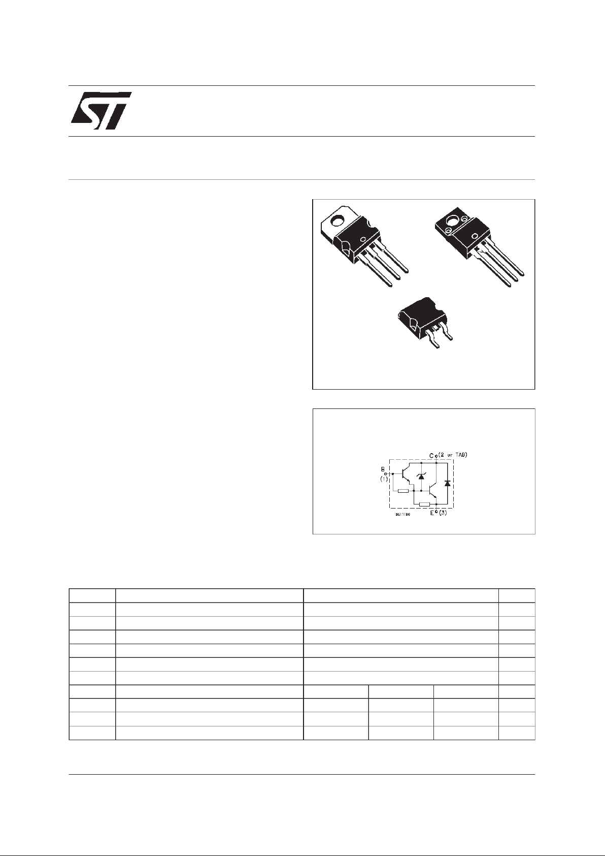
■ WIDERANGE OF PACKAGES
■ SURFACE-MOUNTING D2PAK(TO-263)
POWERPACKAGEIN TUBE (NO SUFFIX)
OR IN TAPE& REEL (SUFFIX ”T4”)
APPLICATIONS
■ HIGH RUGGEDNESSELECTRONIC
IGNITIONS
INTERNAL SCHEMATIC DIAGRAM
January 1999
1
3
D2PAK
TO-263
1
2
3
TO-220
1
2
3
ABSOLUTE MAXIMUM RATINGS
Symb o l Param et e r Val ue Uni t
V
CEO
Collector-Emitter Voltage (IB= 0 ) 350 V
V
EBO
Emitter-Base Voltage (IC=0) 5 V
I
C
Collector Current 15 A
I
CM
Collector Peak Curre nt 30 A
I
B
Base Current 1 A
I
BM
Base Peak Current 5 A
BU941ZT BU941 ZTFP BUB94 1Z T
P
tot
Tot al Dissipat ion at Tc=25oC 150 55 150 W
T
stg
Sto rage Tem pe r ature -65 t o 175 -65 to 175 -65 to 175
o
C
T
j
Max. Operat ing Ju nc t io n T emperat ure 175 175 175
o
C
TO-220FP
1/8
Page 2
THERMAL DATA
TO-220
D2PAK
TO - 2 20FP
R
thj-case
Ther mal Resistan ce Junction- ca s e Max 1 2.7
o
C/W
ELECTRICAL CHARACTERISTICS (T
case
=25oC unlessotherwise specified)
Symbol Parameter Test Condition s Min. Typ. Max. Unit
I
CEO
Collec t or Cut-of f
Current (I
B
=0)
V
CE
=300V
V
CE
=300V Tj=125oC
100
0.5
µA
mA
I
EBO
Emitt er Cut-off Curren t
(I
C
=0)
V
EB
=5V 20 mA
V
CL
∗ Clamping Voltage IC= 10 0 mA 350 500 V
V
CE(sat)
∗ Collect or- Emit t er
Saturation Voltage
IC=8A IB=100mA
I
C
=10A IB=250mA
1.8
1.8
V
V
V
BE(sat)
∗ Ba se-Emi tt er
Saturation Voltage
IC=8A IB=100mA
I
C
=10A IB=250mA
2.2
2.5
V
V
h
FE
∗ DC Current Gain IC=5A VCE= 1 0 V 300
V
F
Diode F orw a rd Voltag e IF=10A 2.5 V
Func tional Test
(see fig. 1)
V
CC
=24V L=7mH 10 A
t
s
t
f
INDUCTIV E LOAD
Storage Time
Fall Time
(see fig. 3)
VCC=12V L=7mH V
clamp
=300V
I
C
=7A IB=70mA
V
BE
=0 RBE=47Ω
15
0.5
µs
µs
∗
Pulsed: Pulse duration = 300 µs, duty cycle 1.5 %
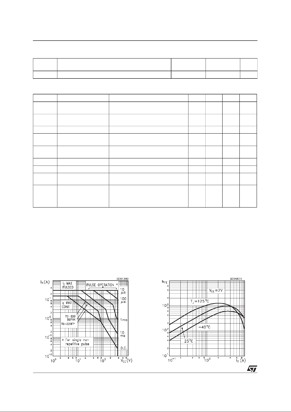
Safe OperatingArea DC Current Gain
BU941ZT / BU941ZTFP / BUB941ZT
2/8
Page 3
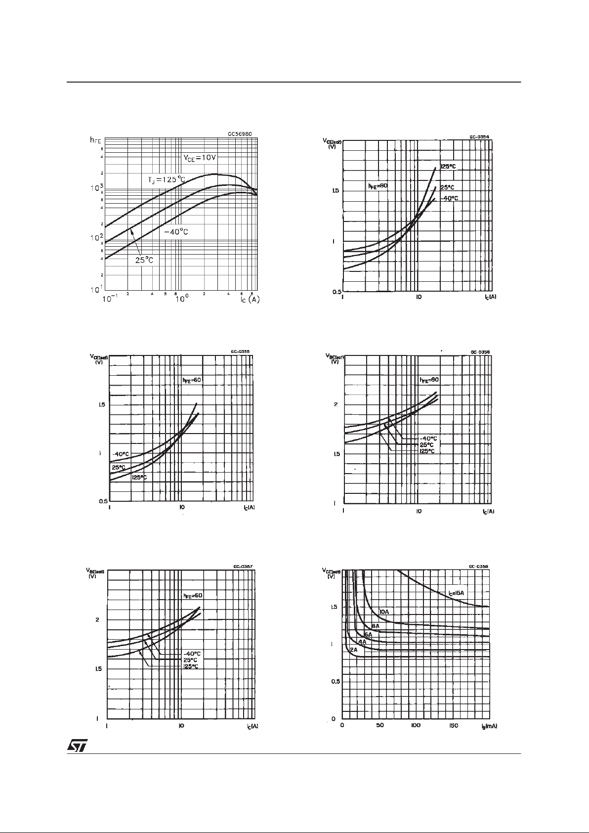
DCCurrent Gain
Collector-emitterSaturation Voltage
Base-emitterSaturation Voltage
Collector-emitterSaturationVoltage
Base-emitterSaturation Voltage
Collector-emitterSaturationVoltage
BU941ZT / BU941ZTFP / BUB941ZT
3/8
Page 4

FIGURE1: Functional Test Circuit FIGURE2: Functional Test Waveforms
FIGURE3: SwitchingTime Test Circuit
BU941ZT / BU941ZTFP / BUB941ZT
4/8
Page 5

DIM.
mm inch
MIN. TYP. MAX. MIN. TYP. MAX.
A 4.40 4.60 0.173 0.181
C 1.23 1.32 0.048 0.051
D 2.40 2.72 0.094 0.107
D1 1.27 0.050
E 0.49 0.70 0.019 0.027
F 0.61 0.88 0.024 0.034
F1 1.14 1.70 0.044 0.067
F2 1.14 1.70 0.044 0.067
G 4.95 5.15 0.194 0.203
G1 2.4 2.7 0.094 0.106
H2 10.0 10.40 0.393 0.409
L2 16.4 0.645
L4 13.0 14.0 0.511 0.551
L5 2.65 2.95 0.104 0.116
L6 15.25 15.75 0.600 0.620
L7 6.2 6.6 0.244 0.260
L9 3.5 3.93 0.137 0.154
DIA. 3.75 3.85 0.147 0.151
P011C
TO-220 MECHANICAL DATA
BU941ZT / BU941ZTFP / BUB941ZT
5/8
Page 6

DIM.
mm inch
MIN. TYP. MAX. MIN. TYP. MAX.
A 4.4 4.6 0.173 0.181
B 2.5 2.7 0.098 0.106
D 2.5 2.75 0.098 0.108
E 0.45 0.7 0.017 0.027
F 0.75 1 0.030 0.039
F1 1.15 1.7 0.045 0.067
F2 1.15 1.7 0.045 0.067
G 4.95 5.2 0.195 0.204
G1 2.4 2.7 0.094 0.106
H 10 10.4 0.393 0.409
L2 16 0.630
L3 28.6 30.6 1.126 1.204
L4 9.8 10.6 0.385 0.417
L6 15.9 16.4 0.626 0.645
L7 9 9.3 0.354 0.366
Ø 3 3.2 0.118 0.126
L2
A
B
D
E
H
G
L6
¯
F
L3
G1
123
F2
F1
L7
L4
TO-220FP MECHANICAL DATA
BU941ZT / BU941ZTFP / BUB941ZT
6/8
Page 7

DIM.
mm inch
MIN. TYP. MAX. MIN. TYP. MAX.
A 4.4 4.6 0.173 0.181
A1 2.49 2.69 0.098 0.106
B 0.7 0.93 0.027 0.036
B2 1.14 1.7 0.044 0.067
C 0.45 0.6 0.017 0.023
C2 1.21 1.36 0.047 0.053
D 8.95 9.35 0.352 0.368
E 10 10.4 0.393 0.409
G 4.88 5.28 0.192 0.208
L 15 15.85 0.590 0.624
L2 1.27 1.4 0.050 0.055
L3 1.4 1.75 0.055 0.068
L2
L3
L
B2
B
G
E
A
C2
D
C
A1
DETAIL”A”
DETAIL”A”
A2
P011P6/E
TO-263 (D2PAK) MECHANICAL DATA
BU941ZT / BU941ZTFP / BUB941ZT
7/8
Page 8

Information furnished isbelieved tobe accurate and reliable. However, STMicroelectronics assumes noresponsibility for the consequences
of use of such information nor for any infringement of patents or other rights of third parties which may result from its use. No license is
granted by implication or otherwise under any patent or patent rights of STMicroelectronics. Specification mentioned in this publication are
subject tochange without notice.This publication supersedes and replaces all information previously supplied. STMicroelectronics products
are not authorized for use as critical components in life support devices or systems without express written approval of STMicroelectronics.
The ST logo is a registered trademark of STMicroelectronics
1998 STMicroelectronics – Printed in Italy – All Rights Reserved
STMicroelectronicsGROUP OF COMPANIES
Australia - Brazil - Canada - China - France -Germany - Italy - Japan - Korea - Malaysia - Malta - Mexico - Morocco - The Netherlands-
Singapore - Spain - Sweden - Switzerland - Taiwan -Thailand - UnitedKingdom - U.S.A.
http://www.st.com
.
BU941ZT / BU941ZTFP / BUB941ZT
8/8
 Loading...