

Page 1
BU941Z/BU941ZP
HIGH VOLTAGE IGNITION COIL DRIVER
■ VERYRUGGED BIPOLARTECHNOLOGY
■ BUILTIN CLAMPINGZENER
■ HIGH OPERATINGJUNCTION
TEMPERATURE
■ WIDERANGE OF PACKAGES
APPLICATIONS
■ HIGH RUGGEDNESSELECTRONIC
IGNITIONS
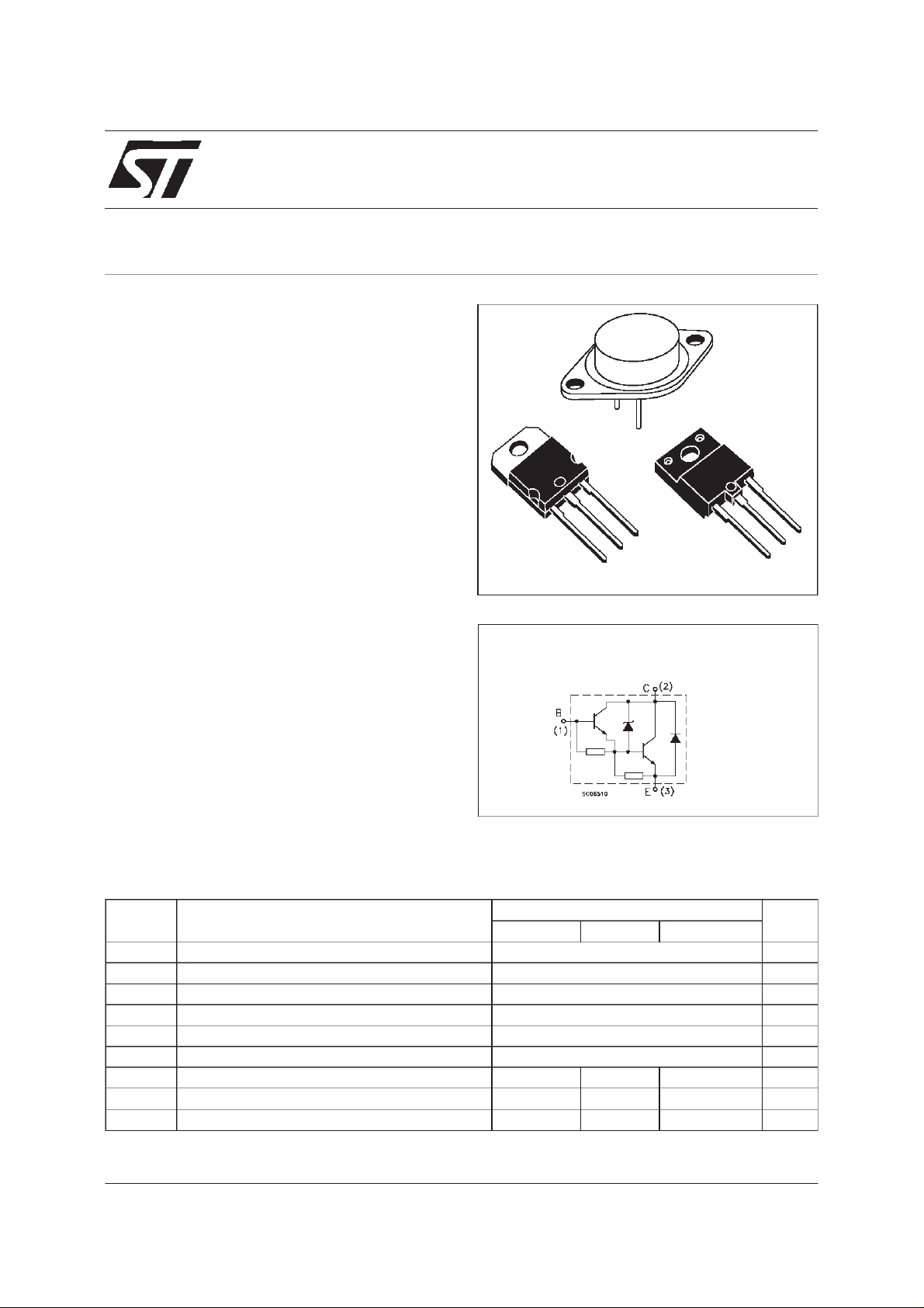
BU941ZPFI
NPN POWER DARLINGTON
TO-3
1
2
3
2
TO-218 ISOWATT218
1
3
2
1
INTERNAL SCHEMATIC DIAGRAM
for TO-3
Emitter: pin 2
Base: pin1
Collector: tab
ABSOLUTE MAXIMUM RATINGS
Symbol Parameter Value Unit
BU941Z BU941ZP BUB9 41Z PFI
V
V
I
I
P
T
Collector-Emitter Voltage (IB= 0 ) 350 V
CEO
Emitter-Base Voltage (IC=0) 5 V
EBO
Collector Current 15 A
I
C
Collector Peak Curre nt 30 A
CM
Base Current 1 A
I
B
Base Peak Current 5 A
BM
Tot al Dissipat ion at Tc=25oC 180 155 65 W
tot
Storage Temperature -65 to 200 -65 to 175 -65 to 175
stg
Max. Operat ing Ju nc t io n T emperat ure 200 175 175
T
j
o
C
o
C
January 2000
1/8
Page 2
BU941Z/BU941ZP/BU941ZPFI
THERMAL DATA
R
thj-case
Thermal Resistance Junction-case Max 0.97 0.97 2.3
TO-3 TO-218 ISOWATT218
o
C/W
ELECTRICAL CHARACTERISTICS (T
=25oC unlessotherwise specified)
case
Symbol Parameter Test Cond ition s Min. Typ. Max. Unit
I
I
V
V
CE(sat)
CEO
EBO
CL
Collec t or Cut-of f
Current (I
B
=0)
Emitt er Cut-off Curren t
(I
=0)
C
∗ Cl am pi ng Voltag e IC= 10 0 mA 350 500 V
∗ Collec t or -Emit t er
Saturation Voltage
V
∗ Base-Emi tter
BE(sat)
Saturation Voltage
h
∗ DC C urrent Gain IC=5A VCE= 1 0 V 300
FE
V
Diode F orw a rd Voltag e IF=10A 2.5 V
F
Func tional Test
V
=300V
CE
=300V Tj=125oC
V
CE
=5V 20 mA
V
EB
IC=8A IB=100mA
=10A IB=250mA
I
C
=12A IB=300mA
I
C
IC=8A IB=100mA
=10A IB=250mA
I
C
=12A IB=300mA
I
C
V
=24V L=7mH 10 A
CC
100
0.5
1.8
1.8
2
2.2
2.5
2.7
(see fig. 1)
INDUCTIV E LOAD
t
s
t
f
Storage Time
Fall Time
(see fig. 3)
∗
Pulsed: Pulse duration = 300 µs, duty cycle 1.5 %
VCC=12V L=7mH
=0 RBE=47Ω
V
BE
=300V IC=7A
V
clamp
I
=70mA
B
15
0.5
µA
mA
V
V
V
V
V
V
µs
µs
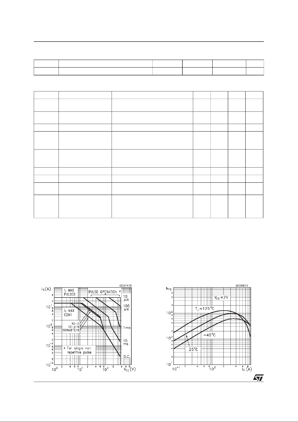
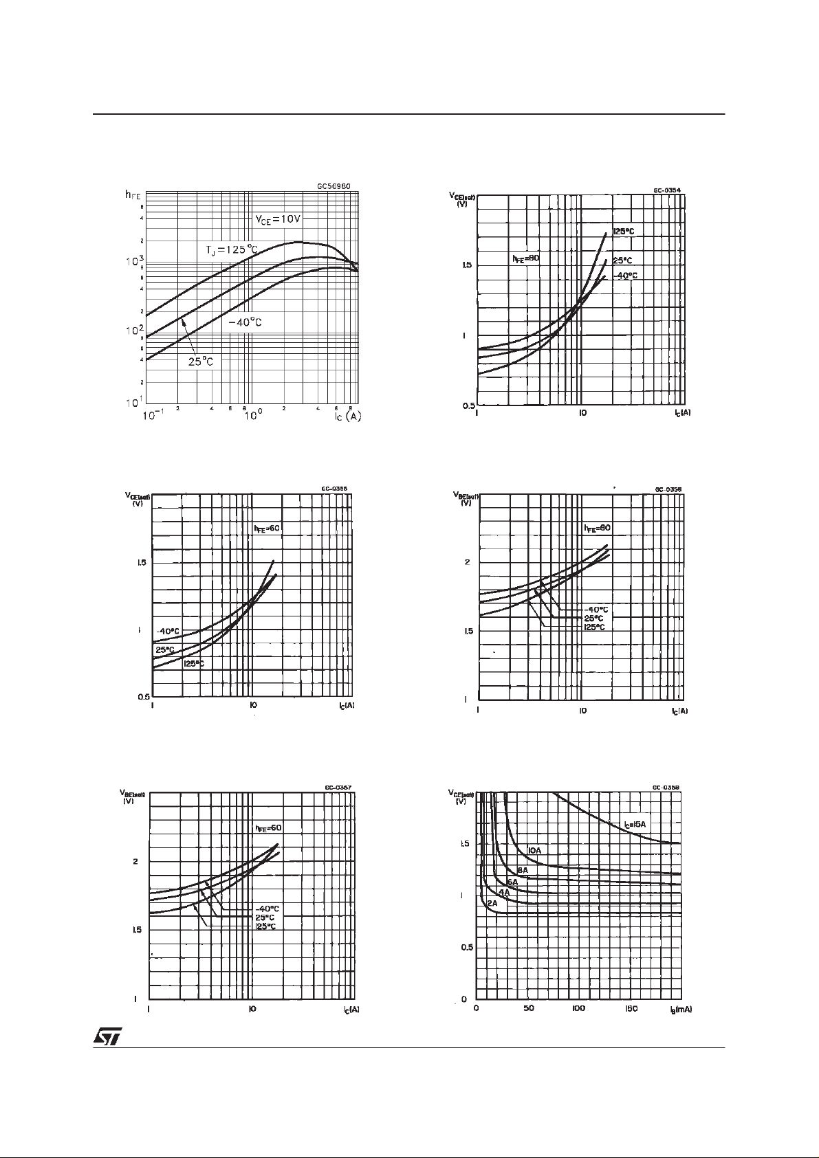
Safe OperatingArea DC Current Gain
2/8
Page 3
BU941Z/BU941ZP/BU941ZPFI
DCCurrent Gain
Collector-emitterSaturation Voltage
Collector-emitterSaturationVoltage
Base-emitterSaturation Voltage
Base-emitterSaturation Voltage
Collector-emitterSaturationVoltage
3/8
Page 4

BU941Z/BU941ZP/BU941ZPFI
FIGURE1: Functional Test Circuit FIGURE2: Functional Test Waveforms
FIGURE3: SwitchingTime Test Circuit
4/8
Page 5

TO-3 MECHANICAL DATA
BU941Z/BU941ZP/BU941ZPFI
DIM.
mm inch
MIN. TYP. MAX. MIN. TYP. MAX.
A 11.00 13.10 0.433 0.516
B 0.97 1.15 0.038 0.045
C 1.50 1.65 0.059 0.065
D 8.32 8.92 0.327 0.351
E 19.00 20.00 0.748 0.787
G 10.70 11.10 0.421 0.437
N 16.50 17.20 0.649 0.677
P 25.00 26.00 0.984 1.023
R 4.00 4.09 0.157 0.161
U 38.50 39.30 1.515 1.547
V 30.00 30.30 1.187 1.193
P
DA
G
U
V
O
N
R
B
C
E
P003F
5/8
Page 6

BU941Z/BU941ZP/BU941ZPFI
TO-218 (SOT-93) MECHANICAL DATA
DIM.
MIN. TYP. MAX. MIN. TYP. MAX.
A 4.7 4.9 0.185 0.193
C 1.17 1.37 0.046 0.054
D 2.5 0.098
E 0.5 0.78 0.019 0.030
F 1.1 1.3 0.043 0.051
G 10.8 11.1 0.425 0.437
H 14.7 15.2 0.578 0.598
L2 – 16.2 – 0.637
L3 18 0.708
L5 3.95 4.15 0.155 0.163
L6 31 1.220
R – 12.2 – 0.480
Ø 4 4.1 0.157 0.161
mm inch
E
A
C
L5
D
L6
L3
L2
H
G
¯
F
R
123
P025A
6/8
Page 7

BU941Z/BU941ZP/BU941ZPFI
ISOWATT218MECHANICAL DATA
DIM.
A 5.35 5.65 0.211 0.222
C 3.30 3.80 0.130 0.150
D 2.90 3.10 0.114 0.122
D1 1.88 2.08 0.074 0.082
E 0.75 0.95 0.030 0.037
F 1.05 1.25 0.041 0.049
F2 1.50 1.70 0.059 0.067
F3 1.90 2.10 0.075 0.083
G 10.80 11.20 0.425 0.441
H 15.80 16.20 0.622 0.638
L 9 0.354
L1 20.80 21.20 0.819 0.835
L2 19.10 19.90 0.752 0.783
L3 22.80 23.60 0.898 0.929
L4 40.50 42.50 1.594 1.673
L5 4.85 5.25 0.191 0.207
L6 20.25 20.75 0.797 0.817
N 2.1 2.3 0.083 0.091
R 4.6 0.181
DIA 3.5 3.7 0.138 0.146
MIN. TYP. MAX. MIN. TYP. MAX.
mm inch
- Weight: 4.9 g (typ.)
- Maximum Torque (applied to mountingflange) Recommended: 0.8 Nm; Maximum: 1 Nm
- The side of thedissipator must beflat within 80 µm
P025C/A
7/8
Page 8

BU941Z/BU941ZP/BU941ZPFI
Information furnished isbelieved tobe accurate and reliable. However, STMicroelectronics assumes noresponsibility for the consequences
of use of such information nor for any infringement of patents or other rights of third parties which may result from its use. No license is
granted by implication or otherwise under any patent or patent rights of STMicroelectronics. Specification mentioned in this publication are
subject tochange without notice.This publication supersedes and replaces allinformation previously supplied. STMicroelectronics products
are not authorized for use as critical components in life support devices or systems without express written approval of STMicroelectronics.
The ST logo is a trademark of STMicroelectronics
2000 STMicroelectronics – Printed in Italy – All Rights Reserved
STMicroelectronicsGROUP OF COMPANIES
Australia - Brazil - China - Finland - France - Germany- Hong Kong - India - Italy- Japan -Malaysia - Malta - Morocco -
Singapore- Spain - Sweden - Switzerland - United Kingdom - U.S.A.
http://www.st.com
8/8
 Loading...