

Page 1
1
Multimedia ICs
KARAOKE echo IC
BU9253AS / BU9253FS / BU9255FS
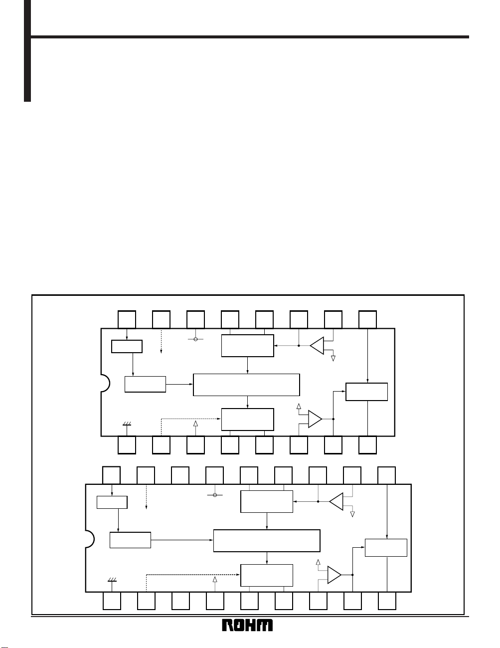
The BU9253AS, BU9253FS and BU9255FS are single-chip ICs that contain all the components needed to configure
a KARAOKE echo system: an A / D and D / A converter, SRAM, LPF, and mixer for mixing source signals. With
these ICs, an echo function can be configured easily and with minimum external components.
•
Applications
KARAOKE functions for portable stereo sets, mini component stereo sets, video CDs and DVDs, etc.
•
Features
1) Echo mixing ratio is adjustable with a DC voltage.
2) A second order LPF can be configured with the
internal amplifier and an attached capacitor and
resistor.
3) Delay time of 131ms. (when f
CLK = 357kHz)
4) Internal mute function.
5) Single power supply (5V).
•
Block diagram
BU9253FS / BU9255FS
BU9253AS
1
COUNTER
V
CC
A / D
SRAM
D / A
OSC
2345678
16 15 14 13 12 11 10 9
MIX
123456789
COUNTER
V
CC
A / D
SRAM
D / A
OSC
16 15 14 13 12 11 10
MIX
18
17
+
–
+
–
+
–
+
–
Page 2
2
Multimedia ICs BU9253AS / BU9253FS / BU9255FS
•
Pin descriptions
BU9253FS / BU9255FS BU9253AS
Pin No. Pin name Function
1
GND
2
ECHO VR
3
BIAS
4
DAINT IN
5
DAINT OUT
6
DALPF IN
7
DALPF OUT
8
MIX OUT
9
MIX IN
10
ADLPF IN
11
ADLPF OUT
12
ADINT OUT
13
ADINT IN
14
V
CC
15
MUTE
16
CR
Analog DC bias
DA integrator input
Echo level DC control
DA integrator output
DA LPF input
DA LPF output
Source sound and echo sound
mixing output
Mixing amplifier source sound input
AD LPF input
AD LPF output
AD integrator output
AD integrator input
Vcc
Mute control
Oscillator output
Ground
•
Absolute maximum ratings (Ta = 25°C)
Parameter Symbol Limits Unit
Applied voltage V
CC 7V
Power dissipation
Pd
500
∗
1
600
∗
2
BU9253FS
BU9253AS
500
∗
1
BU9255FS
mW
Operating temperature Topr – 10 ~
+ 70 °C
Storage temperature Topr – 55 ~
+ 125 °C
Input voltage
VIN – 0.3 ~ VCC + 0.3 V
∗
1 Reduced by 5.0mW for each increase in Ta of 1°C over 25°C.
∗
2 Reduced by 6.0mW for each increase in Ta of 1°C over 25°C.
•
Recommended operating conditions (Ta = 25°C)
Parameter
Power supply voltage V
CC 4.0 5.5 V5.0
Symbol Min. Typ. Max. Unit
Pin No. Pin name Function
1
GND
2
ECHO VR
3
N.C.
4
BIAS
5
DAINT IN
6
DAINT OUT
7
DALPF IN
8
DALPF OUT
9
MIX OUT
10
MIX IN
11
ADLPF IN
12
ADLPF OUT
13
ADINT OUT
14
ADINT IN
15
V
CC
16
17
18
N.C.
MUTE
CR
Ground
Echo level DC control
Internally
Analog DC bias
DA integrator input
DA integrator output
DA LPF input
DA LPF output
Source sound and echo sound
mixing output
Mixing amplifier source sound input
AD LPF input
AD LPF output
AD integrator output
AD integrator input
Vcc
Internally
Mute control
Oscillator output
Page 3

3
Multimedia ICs BU9253AS / BU9253FS / BU9255FS
•
Electrical characteristics (Ta = 25°C, VCC = 5.0V, fCLK = 375kHz, f = 1kHz, VI = - 10dBV, pin 2 = VCC, pin 15 = VCC,
distortion = 400Hz ~ 30kHz filter, output noise voltage : DIN-AUDIO)
*Pin No. are for BU9253FS , BU9255FS and BU9253AS
Parameter
Symbol
Min. Typ. Max. Unit Conditions
V
OM2 1.4 1.7 — Vrms
VNO2 — – 90 – 80 dBV
G
V2 – 1 0 1 dB
G
V1 – 5.6 – 3.5 – 1.4 dB
f
C
— 375 — kHz
V
L
0 — 0.7 V
V
M
1.6 — 2.8 V
V
H
3.8 —
5.0
V
V
OM1 1.4 1.7 — Vrms
VNO1 — – 80 – 60 dBV
THD2 — 0.02 0.1 %
THD1 — 1.5 3 %
I
CC — 6 12 mACurrent consumption
Voltage gain 1
Voltage gain 2
Output distortion 1
Output distortion 2
Output noise voltage 1
Output noise voltage 2
Max. output voltage 1
Max. output voltage 2
Mute control
Oscillation frequency
No signal
Delay total gain
IN1→OUT
Through total gain
IN2→OUT, pin2 = ground
Delay side
Through,
pin2 = ground
Delay,
Rg = 1kΩ
Through side
Rg = 1kΩ, pin2 = ground
Delay,
THD = 10%
Through side, THD = 1%
Pin 2 = ground
H mode hold voltage, pin 15 DC
M mode hold voltage, pin 15 DC
L mode hold voltage, pin 15 DC
Page 4

4
Multimedia ICs BU9253AS / BU9253FS / BU9255FS
•
Measurement circuit (for BU9253FS / BU9255FS)
VCC
VCC
100µ
0.1µ
0.01µ
0.012µ
2.2µ
20k
8.2k
1k
2.2µ
IN1
IN2
1k
4700p
10k
100p
39k
MIX
2.2µ
22k
RESISTOR : [Ω]
Unit
CAPACITOR: [F]
OUT
3300p
15k10k
4.7k
0.01µ
0.01µ
22µ
V
CC
1
2
34
5678
0.47µ
D / A
SRAM
A / DOSC
16 15
14
13
12 11
10
9
COUNTER
+
–
+
–
Fig. 1
Page 5

5
Multimedia ICs BU9253AS / BU9253FS / BU9255FS
• When switching between the muted and unmuted
state (pin 15 (pin 17) L→M→H), the pin 15 (pin 17) M
time should be longer than one SRAM cycle. This is to
assure stability by initializing the SRAM before mode
switching.
Note: Figures in parentheses ( ) are for BU9253AS.
(2) Differences between BU9253AS / FS and BU9255FS
There is a difference regarding the signal stopping for
muting. With BU9253AS / FS, the output from pin 8 (pin
9) is stopped during muting. With BU9255FS, the output
from pin 5 is stopped during muting.
•
Application example (for BU9253FS / BU9255FS)
VCC
VCC
100µ
0.1µ
0.01µ
0.012µ
20k
20k
8.2k
IN
4700p
10k
100p
39k
MUTE
MIX
2.2µ
2.2µ
RESISTOR : [Ω]
Unit
CAPACITOR: [F]
OUT
3300p
15k
10k
4.7k
0.01µ
0.01µ
22µ
ECHO LEVEL
12345678
0.47µ
D / A
SRAM
A / D
OSC
16 15 14 13 12 11 10 9
COUNTER
Fig. 2
+
–
+
–
+
+
+
(1) Mute control functions
H Unmuted (operating state)
M Muted
L Clock stop and muted
Pin 15 voltage (pin 17) Mode
Page 6

6
Multimedia ICs BU9253AS / BU9253FS / BU9255FS
•
External dimensions (Units: mm)
SSOP-A16
0.51Min.
0° ~ 15°
7.62
3.95 ± 0.3
1.778
10
9
6.5 ± 0.3
19.4 ± 0.3
18
1
0.5 ± 0.1
3.4 ± 0.2
0.3
± 0.1
SDIP18
BU9253ASBU9253FS / BU9255FS
0.36 ± 0.10.8
0.11
6.6 ± 0.2
4.4 ± 0.2
6.2 ± 0.31.5 ± 0.1
1
16
8
9
0.15
0.3Min.
0.15 ± 0.1
(3) Setting the echo loop gain
VIN
LPF
R
R
AD SRAM
OdB
V
IN
VO
VDLY
Recommendable gain
+ 3dB
Recommendable gain
– 6dB
R: R = 1: 1
mix
Echo loop ATT V
IN ~ VDLY···A = (A < 1)
∗
With Pin NO. BU9253FS
VIN
VDLY
OUT
DA
2
VR
9
7
8
Fig. 3
+
+
With VOMax being the maximum amplitude of VO at this
time (when the phases, including that of the DLY circuit, are in alignment):
Thus, maximum allowable input is the value of V
OMax
provided the specifications (1 = A). Assuming a feedback ratio (A) of 0.7 and a maximum V
OUT of 4.0 VP-P,
V
IN must be less than 1.2 VP-P.
V
OMax. = (1 + A + A2 + ···) VIN =
1
1-A
∞
Σ
K = 0
A
K
· VIN = VIN
 Loading...