

Page 1
1
Multimedia ICs
PS / 2 Mouse Controller
BU9206
The BU9206 is a PS / 2 mouse communication controller for PCs. This processor shapes waveforms and counts signals from the mouse rotary encoder as the mouse is moved, to provide two-way communication between mouse and
PC system.
•
Applications
PC mouse
•
Features
1) For PS / 2 mouse.
2) Compatible with a wide range of input signals, because it automatically sets the input threshold levels
for the X and Y direction, corresponding to the output level of the rotary encoder inside the mouse.
3) CMOS process enables low current consumption.
•
Absolute maximum ratings (Ta = 25°C)
Parameter
V
DD
Pd
Topr
Tstg
– 0.3 ~ + 7.0
1000
∗
– 25 ~ + 75
– 55 ~ + 125
V
Symbol Limits Unit
mW
°C
°C
VIN – 0.3 ~ VDD + 0.3 V
VOUT – 0.3 ~ VDD + 0.3 V
∗
Reduced by 10 mW for each increase in Ta of 1°C over 25°C.
Power supply voltage
Power dissipation
Operating temperature
Storage temperature
Input voltage
Output voltage
•
Recommended operating conditions (Ta = 25°C)
Parameter
VDD 4.5 5.0 5.5 V VDD
VIH2 0.4∗VDD —VDD V SCLK, SDATA
VIL2 0 — 0.16∗VDD V SCLK, SDATA
VAUP 0.3∗VDD — 0.8∗VDD V XA, XB, YA, YB
VALP 0 — 0.48∗VAUP V XA, XB, YA, YB
SWR, SWL, TEST2B, TEST1B,
TEST0, RESETB
VIH1 0.8∗VDD —VDD V
SWR, SWL, TEST2B, TEST1B,
TEST0, RESETB
VIL1 0 — 0.2∗VDD V
Symbol Min. Typ. Max. Unit Application pin
Power supply voltage
H input voltage 1
H input voltage 2
L input voltage 1
L input voltage 2
XY input H voltage
XY input L voltage
Page 2
2
Multimedia ICs BU9206
•
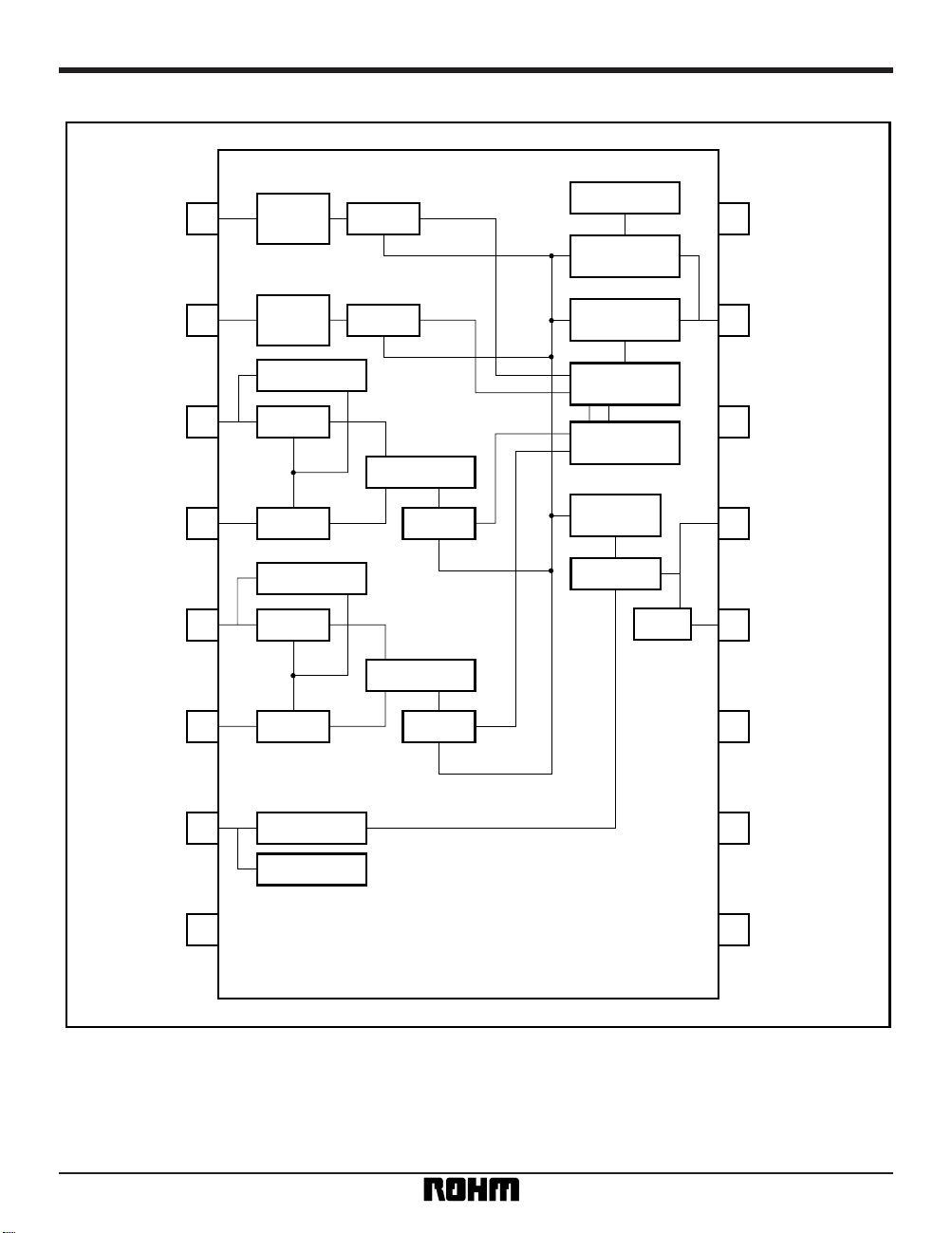
Block diagram
1
2
3
4
5
6
7
8
SWR
SWL
XA
XB
YA
YB
SCLK
V
SS
VDD
SDATA
RESETB
OSC1
OSC2
TEST0
TEST1B
TEST2B
16
15
14
13
12
11
10
9
Peak det.
Accumlator
Comp.
Comp.
Peak det.
Accumlator
Comp.
Comp.
Regi.
SCLK gen.
I / O inhibit
Osc
Data decoder
Data shifter
for output
Data shifter
for input
Scaling and
turbo
Sample
timing
Data encoder
Clk gen.
Regi.
Latch
Latch
Noise
cancel
Noise
cancel
Page 3

3
Multimedia ICs BU9206
•
Pin descriptions
Pin No.
Pin name
SWR1IN
I / O I / O formatFunction
Right switch input
Pull-up resistor built in
Low active
Left switch input
Pull-up resistor built in
Low active
Serial clock input / output
Pull-up resistor built in
Open drain output
Tip test input
Pull-up resistor built in
Low active
Normally open or connected to V
DD
Pull-up resistor built in
Normally connected to GND
SWL2IN
XA3IN
Rotary encoder X-direction, A-phase input
Rotary encoder X-direction, B-phase input
Rotary encoder Y-direction, A-phase input
Rotary encoder Y-direction, B-phase input
XB4IN
YA5IN
YB6IN
SCLK7 I / O
V
SS
8— —
Input / output reference voltage: 0V
TEST2B9IN
TEST1B10 IN
TEST011 IN
SWR
SWL
XA
XB
YA
YB
Typ.38kΩ
TEST1B
TEST2B
Typ.11kΩ
TURBO
Typ.38kΩ
Typ.5kΩ
Vref
COMP
+
–
Page 4

4
Multimedia ICs BU9206
Pin No.
Pin name
OSC212 IN
I / O I / O formatFunction
Pin to connect oscillator for clock
Connect a 4MHz oscillator between
OSC1 and OSC2.
OSC113 OUT
RESETB14 IN
Reset input
Pull-up resistor built in
Low active
SDATA15 I / O
V
DD16 — —
Power supply pin
Connect a 4.5 - 5.5V power supply.
Serial data input / output
Pull-up resistor built in
Open drain output
RESETB
OSC2 OSC1
SDATA
Typ.38kΩ
Typ.5kΩ
Page 5

5
Multimedia ICs BU9206
•
Electrical characteristics (unless otherwise noted, Ta = 25°C, VDD = 5.0V)
Parameter
Symbol Conditions Applied pin
IDD fCK = 4.0MHz VDD
Min.
0.5
Typ.
2.1
Max.
4.0
Unit
mA
VOL1 ISINK = 4.0mA SCLK, SDATA— 0.43 0.6 V
IIL1 VIN = VSS SWR, SWL, TEST0, RESETB98 130 195 µA
IIL2 VIN = VSS TEST1B, TEST2B330 440 660 µA
IIL3 VIN = VSS SCLK, SDATA0.75 1.0 1.5 mA
IIL4 VIN = VSS XA, XB, YA, YB——10µA
IIH1 VIN = VDD SWR, SWL, TEST0, RESETB——10µA
IIH2 VIN = VDD TEST1B, TEST2B——10µA
IIH3 VIN = VDD SCLK, SDATA——10µA
IIH4 VIN = VDD XA, XB, YA, YB——10µA
IOSC VIN = GND or VDD OSC2— ± 6 ± 20 µA
fOSCOscillation frequency OSC1— 4.0 — MHz
Supply current
Output low level voltage 1
Input low level current 1
Input low level current 2
Input low level current 3
Input low level current 4
Input high level current 1
Input high level current 2
Input high level current 3
Input high level current 4
OSC2 input current
•
Application circuit
1
2
3
4
5
6
7
8
SWR
SWL
XA
XB
YA
YB
SCLK
V
SS
VDD
SDATA
V
SS
SCLK
V
DD
SDATA
RESETB
OSC1
OSC2
TEST0
TEST1B
TEST2B
16
15
14
13
12
11
10
9
Fig. 1
Page 6

6
Multimedia ICs BU9206
•
External dimensions (Units: mm)
DIP16
0.51Min.
0.3
± 0.1
916
81
6.5 ± 0.3
3.2
±
0.2
4.25
±
0.3
0.5 ± 0.1
19.4 ± 0.3
2.54
0° ~ 15°
7.62
 Loading...