

Page 1
1
Multimedia ICs
Clock generator for personal
computers
BU2192F
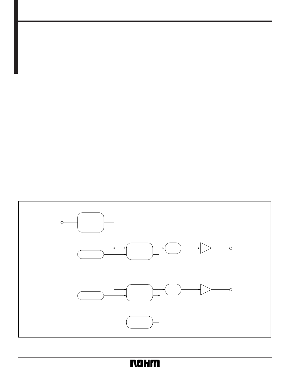
The BU2192F is a clock generator IC for personal computers, and uses a single crystal resonator to generate the
three clock signals needed for personal computers.
•
Applications
Personal computers
•
Features
1) Clock signals of two different types can be generated with a single attached crystal generator.
2) Internal PLL loop filter, eliminating the need for an
attached component.
3) Single 5V power supply.
4) SOP 8-pin package.
•
Block diagram
XTAL
OSC
DATA1
DATA2
PLL1
1 / 2
1 / 4
CLK1
33.8680MHz
24.5795MHz
CLK2
PLL2
VREF
XTAL1
14.3181MHz
Page 2
2
Multimedia ICs BU2192F
•
Pin descriptions
Pin No. Pin name Function Circuit
1
2
3
4
5
6
7
8
CLK2
GND
XTAL I
N.C.
CLK1
N.C.
DV
DD
AVDD
Clock output 2 (f2 = 24.5795MHz)
GND
Reference oscillation input
Clock output 1 (f1 = 33.8680MHz)
Digital power supply
Analog power supply
A
—
B
—
A
—
—
—
—
—
•
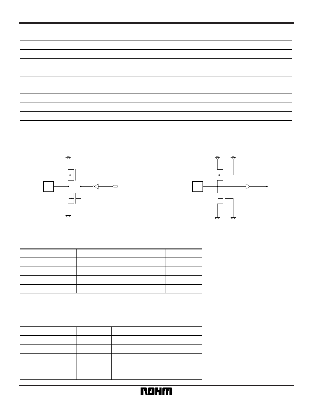
Input / output circuits
Pin
From inside
Pin
To inside
Type A Type B
1 • 5 3
•
Absolute maximum ratings (Ta = 25°C)
•
Recommended operating conditions (Ta = 25°C)
Parameter Symbol Limits Unit
Applied voltage
Input voltage
Storage temperature
Power dissipation
V
DD
VIN
Tstg
Pd
– 0.5 ~ + 7.0
– 0.5 ~ V
DD + 0.5
– 30 ~ + 125
450
∗
V
V
°C
mW
䊊 Do not represent guaranteed performance.
∗
Reduced by 4.5mW for each increase in Ta of 1°C over 25°C.
䊊 Not designed for radiation resistance.
Parameter Symbol Limits Unit
Power supply voltage
Input high level voltage
Input low level voltage
Operating temperature
Output load
V
DD
VIH
VIL
Topr
CL
– 4.5
0.8 × V
DD
0.0
– 5
~ + 5.5
~ V
DD
~ 0.2 × VDD
~ + 70
V
V
V
°C
pF
15 (Max.)
Page 3

3
Multimedia ICs BU2192F
•
Electrical characteristics (unless otherwise noted, Ta = 0 to 70°C, VDD (AVDD) = 4.5V to 5.5V, CL ⬉ 15pF,
XTALI [f
REF] = 14.3181MHz)
Parameter
Symbol Min. Typ. Max. Unit Conditions
Input Vth XTALI
Output low level voltage
Output high level voltage
Operating circuit current
Output frequency 1
Output frequency 2
Rise time
Fall time
Jitter
Jitter
Power up time
Duty
V
th
VOL
VOH
IDD
f1
f2
tR
tF
J1s
Jabs
t
PT
Duty
0.8
—
VDD – 0.5
—
– 100ppm
– 100ppm
—
—
—
—
—
45
—
—
—
30
33.8680
24.5795
—
—
80
300
—
50
—2.2
0.4
—
50
+ 100ppm
+ 100ppm
5
5
250
1
10
55
V
V
V
mA
MHz
MHz
nsec
nsec
psec
nsec
msec
%
l
OL = 4.0mA
l
OL = – 4.0mA
f
REF = 14.3181MHz, no load
f
REF × 123 / 26 / 2
f
REF × 103 / 15 / 4
V
DD × 0.2 to VDD × 0.8
V
DD × 0.8 to VDD × 0.2
1sigma
MIN-MAX width
∗
Measure with Vth = 1 / 2VDD
∗
The time for the output to stabilize after the power supply reaches 90% after being turned on.
However, if the power supply rise (to rise condition) takes the entire time, this requirement is satisfied.
•
Application example
CLK2
GND
XTALI
N.C.
AV
DD
DVDD
N.C.
CLK1
0.1µF
33.8680MHz
24.5795MHz
f
REF = 14.3181MHz
1 8
27
36
45
Page 4

4
Multimedia ICs BU2192F
SOP8
0.4 ± 0.11.27
0.15
0.3Min.
0.15 ± 0.1
0.11
6.2 ± 0.3
4.4 ± 0.2
5.0 ± 0.2
85
41
1.5 ± 0.1
•
External dimensions (Units: mm)
 Loading...