

Page 1
现货库存、技术资料、百科信息、热点资讯,精彩尽在鼎好!
FEATURES
.HIGHSURGECAPABILITY
.HIGH ON-STATECURRENT
.HIGH STABILITYAND RELIABILITY
.BTW68 Serie :
INSULATEDVOLTAGE= 2500V
(ULRECOGNIZED: E81734)
DESCRIPTION
The BTW 68 (N) Family of Silicon Controlled Rectifiers uses a high performance glass passivated
technology.
This general purpose Family of Silicon Controlled
Rectifiers is designed for power supplies up to
400Hz on resistive or inductive load.
(RMS)
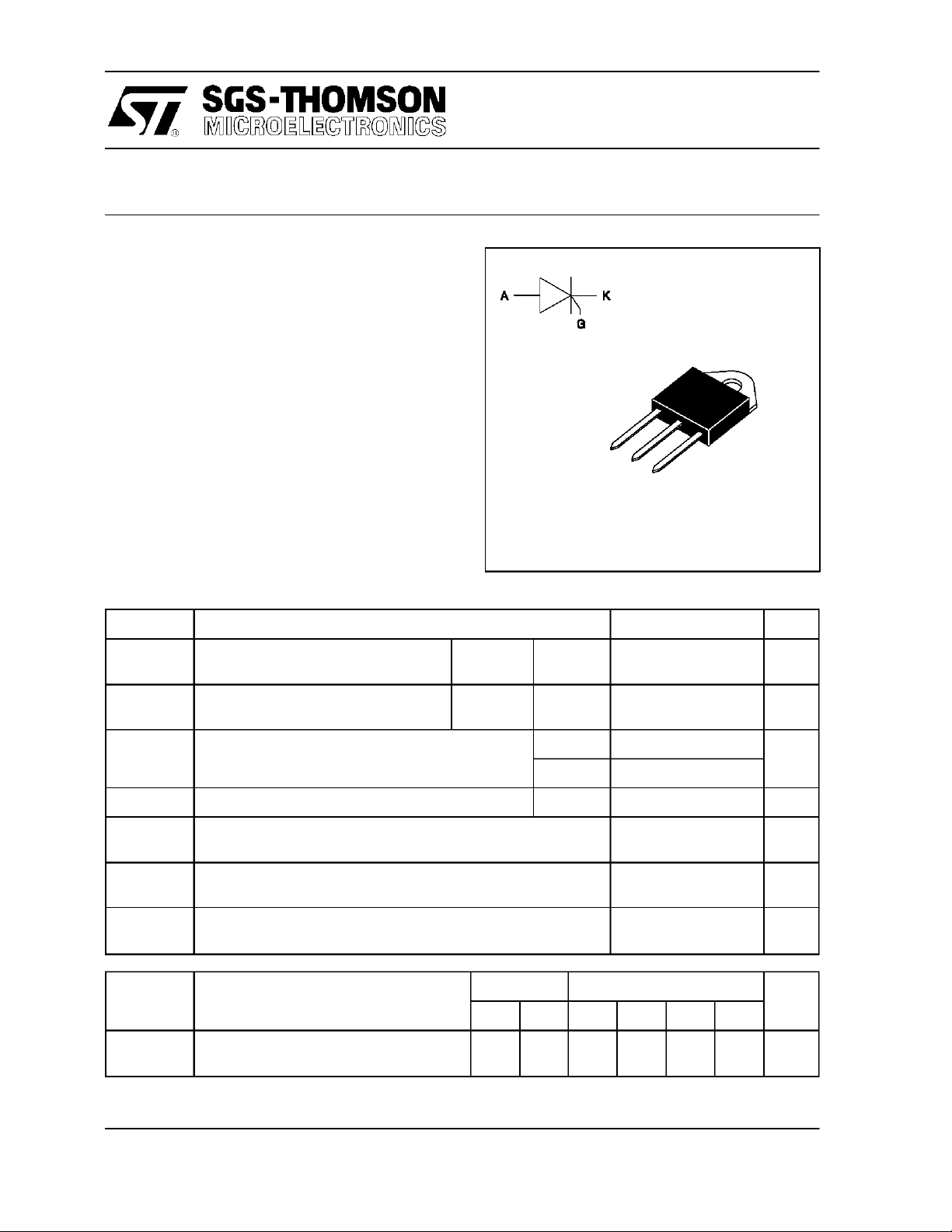
BTW 68 (N)
K
A
G
TOP 3
(Plastic)
SCR
ABSOLUTE RATINGS (limitingvalues)
Symbol Parameter Value Unit
I
T(RMS)
I
T(AV)
I
TSM
I2tI
dI/dt Critical rate of rise of on-state current
Tstg
Tj
Tl Maximum lead temperature for soldering during 10 s at 4.5 mm
Symbol Parameter BTW 68 BTW 68 / BTW 68 N Unit
RMS on-state current
(180° conduction angle)
Average on-state current (180°
conduction angle,single phase circuit)
Non repetitive surge peak on-state current
( Tj initial = 25°C)
2
t value tp=10 ms 800 A2s
Gate supply : IG= 100 mA diG/dt = 1 A/µs
Storage and operating junction temperature range - 40 to + 150
from case
BTW 68
BTW 68 N
BTW 68
BTW 68 N
200 400 600 800 1000 1200
Tc=80°C
Tc=85°C
Tc=80°C
Tc=85°C
tp=8.3 ms 420 A
tp=10 ms 400
30
35
19
22
100 A/µs
- 40 to + 125
230 °C
A
A
°C
°C
V
DRM
V
RRM
March 1995
Repetitive peak off-state voltage
Tj = 125 °C
200 400 600 800 1000 1200 V
1/5
Page 2
BTW 68 (N)
THERMAL RESISTANCES
Symbol Parameter Value Unit
Rth (j-a) Junction to ambient 50 °C/W
Rth (j-c) DC Junction to case for DC BTW 68 1.1 °C/W
BTW 68 N 0.8
GATECHARACTERISTICS (maximumvalues)
P
ELECTRICAL CHARACTERISTICS
=1W PGM= 40W (tp = 20 µs) I
G (AV)
Symbol Test Conditions Value Unit
= 8A (tp = 20 µs) V
FGM
RGM
=5V.
BTW 68 BTW 68 N
I
GT
V
GT
V
GD
tgt VD=V
I
L
I
H
V
TM
I
DRM
I
RRM
dV/dt Linear slope up to
tq VD=67%V
VD=12V (DC) RL=33Ω Tj=25°C MAX 50 mA
VD=12V (DC) RL=33Ω Tj=25°C MAX 1.5 V
VD=V
DRMRL
DRMIG
dIG/dt = 1.5A/µs
IG= 1.2 I
IT= 500mA gate open Tj=25°C MAX 75 mA
BTW 68 ITM= 60A
BTW 68 N ITM= 70A tp= 380µs
V
V
VD=67%V
gate open
dITM/dt=30 A/µsdV
DRM
RRM
GT
Rated
Rated
DRM
DRMITM
=3.3kΩ Tj= 125°C MIN 0.2 V
= 200mA
= 60A VR= 75V
/dt= 20V/µs
D
V
V
DRM
DRM
≤ 800V
≥ 1000V
Tj=25°C TYP 2 µs
Tj=25°C TYP 40 mA
Tj=25°C MAX 2.1 2.2 V
Tj=25°C MAX 0.02 mA
Tj= 125°C6
Tj= 125°C MIN 500
250
Tj= 125°C TYP 100 µs
V/µs
2/5
Page 3

BTW 68 (N)
Package I
BTW 68
(Insulated)
BTW 68 N
(Uninsulated)
Fig.1 : Maximum average power dissipation versus
average on-state current (BTW 68).
T(RMS)
A V BTW
30 200 X
35 600 X
V
DRM/VRRM
Sensitivity Specification
400 X
600 X
800 X
1000 X
1200 X
800 X
1000 X
1200 X
Fig.2 : Correlation between maximum average power
dissipation and maximum allowable temperatures (T
and T
contact (BTW 68).
) for different thermal resistances heatsink +
case
amb
Fig.3 : Maximum average power dissipation versus
average on-state current (BTW 68 N).
Fig.4 : Correlation between maximum average power
dissipation and maximum allowable temperatures (T
and T
contact (BTW 68 N).
) for different thermal resistances heatsink +
case
amb
3/5
Page 4

BTW 68 (N)
Fig.5 : Average on-state current versus case
temperature (BTW 68).
Fig.7 : Relative variation of thermal impedance versus
pulse duration.
Zth/Rth
1.00
Zth(j-c)
Fig.6 : Average on-state current versus case
temperature (BTW 68 N).
Fig.8 : Relative variation of gate trigger current versus
junction temperature.
0.10
Zth( j-a)
0.01
tp(s)
1E-3 1E-2 1E-1 1E+0 1 E+1 1E+2 1E+3
Fig.9 : Non repetitive surge peak on-state current
versus number of cycles.
Fig.10 : Non repetitive surge peak on-state current for a
sinusoidal pulse with width : t ≤ 10 ms, and
corresponding value of I2t.
4/5
Page 5

Fig11 : On-state characteristics (maximum values).
PACKAGE MECHANICAL DATA
TOP3 Plastic
A
R4.6
G
P
NN
I
D
B
J
L
M
BTW 68 (N)
REF. DIMENSIONS
H
A 15.10 15.50 0.594 0.611
B 20.70 21.10 0.814 0.831
C 14.30 15.60 0.561 0.615
D 16.10 16.50 0.632 0.650
G 3.40 - 0.133 -
H 4.40 4.60 0.173 0.182
C
L 0.50 0.70 0.019 0.028
M 2.70 2.90 0.106 0.115
N 5.40 5.65 0.212 0.223
P 1.20 1.40 0.047 0.056
Millimeters Inches
Min. Max. Min. Max.
I 4.08 4.17 0.161 0.164
J 1.45 1.55 0.057 0.062
Cooling method : C
Marking : type number
Weight : 4.7 g
Information furnished is believed to be accurate and reliable. However, SGS-THOMSON Microelectronics assumes no responsability
for the consequences of use of such information nor for any infringement of patents or other rights of third parties which may
result from its use. No license is granted by implication orotherwise under any patent or patent rights of SGS-THOMSON Microelectronics.
Specifications mentioned in this publication are subject to change without notice. This publication supersedes and replaces all
information previously supplied.
SGS-THOMSON Microelectronics products are not authorized for use as critical components in life support devices or systems
without express written approval of SGS-THOMSON Microelectronics.
Recommended torque value : 0.8 m.N.
Maximum torque value : 1 m.N.
1995 SGS-THOMSON Microelectronics - Printed in Italy - All rights reserved.
SGS-THOMSON Microelectronics GROUP OF COMPANIES
Australia - Brazil - France - Germany - Hong Kong - Italy - Japan - Korea - Malaysia - Malta - Morocco - The Nether-
lands Singapore - Spain - Sweden - Switzerland - Taiwan - Thailand - United Kingdom - U.S.A.
5/5
 Loading...