

Page 1
BTW67 and BTW69 Series
STANDARD 50A SCRs
MAIN FEATURES:
Symbol Value Unit
I
T(RMS)
V
DRM/VRRM
I
GT
50 A
600to1200 V
80 mA
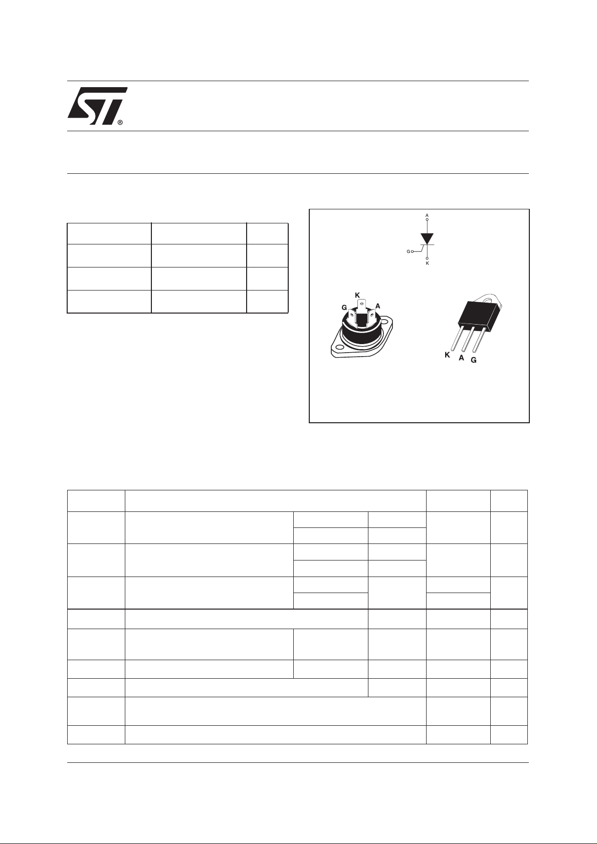
DESCRIPTION
Available in high power packages, the BTW67 /
BTW69 Series is suitable in applications where
power handling and power dissipation are critical,
such as solid state relays, welding equipment,
high power motor c ontrol.
RD91
(BTW67)
TOP3
(BTW69)
Based on a clip assembly technology, they offer a
superior performance in surge current handling
capabilities.
Thanks to their internal ceramic pad, they provide
high voltage insulation (2500V RMS), com plying
with UL standards (file ref: E81734).
ABSOLUTE RATINGS (limiting values)
Symbol Parameter Value Unit
I
T(RMS)
I
T(AV)
I
TSM
²
I
tI
dI/dt
I
GM
P
G(AV)
T
stg
Tj
V
RGM
RMS on-state current
(180° conduction angle)
Average on-state current
(180° conduction angle)
Non repetitivesurge peakon-statecurrent tp = 8.3 ms
²
t Value for fusing
Critical rate of rise of on-state current I
,tr≤100 ns
2xI
GT
Peak gate current tp = 20 µs Tj = 125°C 8 A
Average gate power dissipation Tj = 125°C 1 W
Storage junction temperature range
Operating junction temperature range
Maximum peak reverse gate voltage 5 V
=
G
RD91 Tc = 70°C
50 A
TOP3 Ins. Tc = 75°C
RD91 Tc = 70°C
32 A
TOP3 Ins. Tc = 75°C
610
Tj = 25°C
tp = 10 ms 580
Tj = 25°C 1680
F = 60 Hz Tj = 125°C 50 A/µs
-40to+150
-40to+125
A
2
A
S
°C
April 2001 - Ed: 4
1/5
Page 2
BTW67 and BTW69 Series
ELECTRICAL CHARACTERISTICS (Tj = 25°C, unless otherwise specified)
Symbol Test Conditions Value Unit
I
GT
VD=12V RL=33Ω
V
GT
V
GD
I
H
I
L
dV/dt V
V
TM
V
t0
R
d
I
DRM
I
RRM
VD=V
DRMRL
=3.3kΩ
IT=500mA Gateopen
IG=1.2I
=67%V
D
GT
DRM
Gate open
ITM=100A tp=380µs
Threshold voltage Tj = 125°C MAX. 1.0 V
Dynamic resistance Tj = 125°C MAX. 8.5 mΩ
V
DRM=VRRM
Tj = 125°C MIN.
Tj = 125°C MIN. 1000 V/µs
Tj = 25°C MAX. 1.9 V
Tj = 25°C MAX. 10 µA
Tj = 125°C 5 mA
THERMAL RESISTANCES
Symbol Parameter Value Unit
R
th(j-c)
R
th(j-a)
Junction to case (DC) RD91 (Insulated) 1.0 °C/W
Junction to ambient
MIN. 8
MAX. 80
MAX. 1.3 V
0.2 V
MAX. 150 mA
MAX.
200
TOP3 Insulated 0.9
TOP3 Insulated 50
mA
mA
°C/W
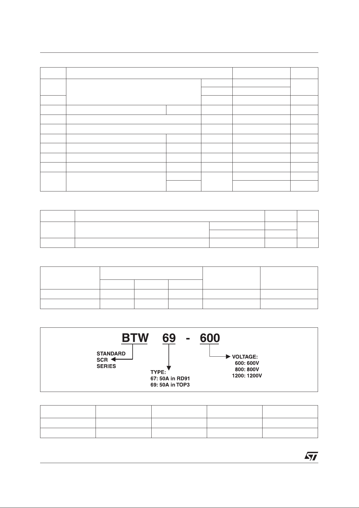
PRODUCT SELECTOR
PartNumber
600 V 800 V 1200 V
BTW67-xxx X X X 80 mA RD91
BTW69-xxx X X X 80 mA TOP3 Ins.
Voltage (xxx)
Sensitivity
Package
ORDERING INFORMATION
OTHER INFORMATION
Part Number Marking Weight Base Quantity Packing mode
BTW67-xxx BTW67xxx 20.0 g 25 Bulk
BTW69-xxx BTW69xxx 4.5 g 120 Bulk
Note:xxx=voltage
2/5
Page 3

BTW67 and BTW69 Series
Fig. 1: Maximum average power dissipation
versus average on-state curr ent.
Fig. 3: Relative variation of thermal impedance
versus pulse duration.
Fig. 2: Average and D.C. on-state current versus
case temperature.
Fig. 4: Relative variation of gate trigger current,
holding current and latching current versus
junction temperature.
Fig. 5: Surge peak on-state current versus
number of cycles.
Fig. 6: Non-repetitive surge peak on-st ate
current for a sinusoidal pulse with width
tp < 10ms, and corresponding value of I²t.
3/5
Page 4

BTW67 and BTW69 Series
Fig. 7: On-state characteristics (maximum
values).
PACKAGE MECHANICAL DATA
RD91 (Plastic)
DIMENSIONS
REF.
A 40.00 1.575
A1 29.90 30.30 1.177 1.193
A2 22.00 0.867
B 27.00 1.063
B1 13.50 16.50 0.531 0.650
B2 24.00 0.945
C 14.00 0.551
C1 3.50 0.138
C2 1.95 3.00 0.077 0.118
E3 0.70 0.90 0.027 0.035
F 4.00 4.50 0.157 0.177
I 11.20 13.60 0.441 0.535
L1 3.10 3.50 0.122 0.138
L2 1.70 1.90 0.067 0.075
N1 33° 43° 33° 43°
N2 28° 38° 28° 38°
Millimeters Inches
Min. Max. Min. Max.
4/5
Page 5

PACKAGE MECHANICAL DATA
TOP3 Ins.(Plastic)
BTW67 and BTW69 Series
Information furnished is believed to be accurate and reliable. However, STMicroelectronics assumes no responsibility for
the consequences of use of such information nor for any infringement of patents or other rights of third parties which may
result from its use. No license is granted by implication or otherwise under any patent or patent rights of
STMicroelectronics. Specifications mentioned in this publication are subject to change without notice. This publication
supersedes and replaces all information previously supplied.STMicroelect ronics products are not authorized for use as
critical components in life support devices or systems without express written approval of STMicroelectronics.
© The ST logo is a registered trademark of STMicroelectronics
© 2001 STMicroelectronics - Printed in Italy - All rights reser ved
.
STMicroelectronics GROUP OF COMPANIES
Australia - Brazil - China - Finland - France - Germany - Hong Kong - India - Italy - Japan - Malaysia-Malta - Morocco
Singapore - Spain - Sweden - Switzerland - United Kingdom - U.S.A.
http://www.st.com
5/5
 Loading...