

Page 1
Smart Highside High Current Power Switch
)
PROFET® BTS650P
Features
•
Overload protection
•
Current limitat ion
•
Short circuit pr otection
•
Overtemperature protection
•
Overvoltage protection (including load dump)
•
Clamp of negative volt age at output
•
Fast deenergizing of induc tive loads
•
Low ohmic inverse current operation
•
Reverse battery pr otection
•
Diagnostic feedback with load current sense
•
Open load detection via c ur r ent sense
•
Loss of
•
Electrostatic discharge (ESD) protection
V
protection
bb
2
)
1
)
Application
•
Power switch with c ur r ent sense diagnostic
feedback for 12
•
Most suitable f or loads with high inrush current
like lamps and motors; all types of resis tive and
inductive loads
•
Replaces electromechanic al r elay s , fuses and
discrete circuits
V and 24 V DC grounded loads
Product Summary
Overvoltage protection
Output clamp
Operating voltage
On-state resistance
Load current (ISO)
Short circuit current l i m i t ation
Current sense ratio
TO-220AB/7
1
Standard
V
bb(AZ)
V
ON(CL
V
bb(on)
R
ON
I
L(ISO)
I
L(SC)
I
L :
7
I
IS
62 V
5.0 ... 34 V
6.0
70 A
130 A
14 000
1
SMD
42
V
mΩ
7
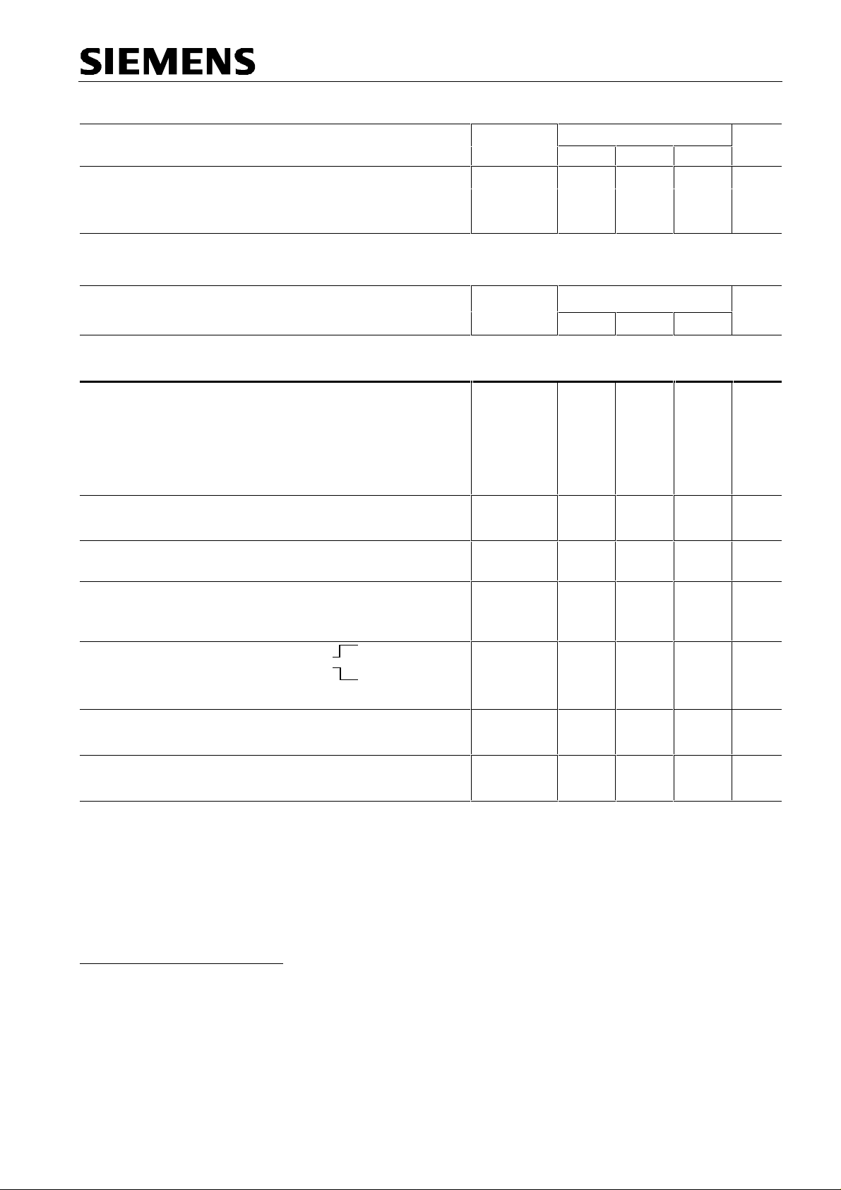
General Description
N channel vertical power F E T with charge pump, cur r ent controlled input and diagnost ic feedback with load
current sense, integrated in Smart S IPMOS chip on chip technology. Fully protected by em bedded pr otection
functions.
4 & Tab
+ V
R
Voltage
source
Voltage
sensor
3
IN
ESD
I
IN
V
IN
V
IS
Logic
I
IS
IS
5
R
IS
Overvoltage
protection
Charge pump
Level shifter
Rectifier
Current
limit
Gate
protection
Limit for
unclamped
ind. loads
Output
Voltage
detection
Temperature
sensor
bb
Current
Sense
PROFET
bb
OUT
1,2,6,7
I
L
Load GND
Load
Logic GND
1
) With additional ext er nal diode.
2
)
Additional external diode requir ed for energized inductive loads ( s ee page 9) .
Semiconductor Group Page 1 of 16 1998-Nov.-2
Page 2

Pin Symbol Function
1OUTO
Output to the load. The pins
especially in high current applic ations!
BTS650P
1,2,6 and 7 must be s hor ted with each other
3
)
2 OUT O Output to the load. The pins 1,2, 6 and 7 m us t be shorted with each ot her
especially in high current applic ations!
3 IN I Input, act iv ates the power switch in c as e of short to ground
4V
5ISS
6OUTO
7OUTO
Maximum Ratings at
bb
T
Positive power supply v oltage, the tab is electrically connected t o this pin.
+
In high current applications the tab should be used f or the V
instead of this pin
Diagnostic feedback pr ov iding a s ens e c ur r ent proportional to the load
current; zer o c ur r ent on failure (see Truth Table on page 7)
Output to the load. The pins
especially in high current applic ations!
Output to the load. The pins
especially in high current applic ations!
j = 25 °C unless otherwise specified
4
)
.
1,2,6 and 7 must be s hor ted with each other
1,2,6 and 7 must be s hor ted with each other
3)
connection
bb
3)
3)
Parameter Symbol Values Unit
Supply voltage (overvoltage protect ion s ee page 4)
Supply voltage for short circuit protection,
T
=-40 ...+150°C: (see diagram on page 10)
j,start
Load current (short circuit current, see page 5)
Load dump protection
5
)
R
= 2 Ω,
I
R
= 0.54 Ω,
L
V
LoadDump
t
= 200 ms,
d
=
V
A
+
V
,
s
V
= 13.5 V
A
V
bb
V
bb
I
L
V
Load dump
42 V
34 V
self-limited A
6
)
75 V
IN, IS = open or grounded
Operating temperature range
Storage temperature range
Power dissipation (DC), TC ≤ 25 °C
T
T
P
j
stg
tot
-40 ...+150
-55 ...+150
170 W
°C
Inductive load switch-off energy dissipation, single pulse
V
= 12V,
bb
I
= 20 A, ZL = 7.5 mH, 0 Ω, see diagrams on page 10
L
Electrostatic discharge capability (ESD)
Human Body Model acc. M IL-STD883D, met hod 3015.7 and ESD
assn. std. S 5.1-1993, C = 100 pF, R = 1.5 kΩ
Current through input pin (DC)
Current through current sense status pin (DC)
see internal circuit diagr am s on page 7 and 8
T
j,start
= 150°C,
T
= 150°C const.,
C
E
V
I
I
AS
ESD
IN
IS
1.5 J
+15 , -250
+15 , -250
4kV
mA
3
)
Not shorting all outputs will considerably increase the on-state resis tance, reduce the peak c ur r ent
capability and decrease t he c ur r ent sense accuracy
4
)
Otherwise add up to 0.7 mΩ (depending on used length of the pin) to the RON if the pin is used inst ead of
the tab.
5
)
R
= internal resis tance of the load dump tes t pulse generator.
I
6
)
V
Load dump
is setup without the DUT connected to the generator per ISO 7637-1 and DIN 40839.
Semiconductor Group Page 2 1998-Nov.-2
Page 3
BTS650P
Thermal Characteristics
Parameter and Conditions Symbol Values Unit
min typ max
7
)
Thermal resistance chip - case:
junction - ambient (free air):
SMD version, device on PCB
8
R
thJC
R
thJA
)
:33
-- -- 0.75
--
60 --
K/W
Electrical Characteristics
Parameter and Conditions Symbol Values Unit
at
T
j = -40 ... +150 °C,
Load Switching Capabilities and Characteristics
On-state resistance (Tab to pins 1,2, 6,7, see
measurement circ uit page 7)
Nominal load current
ISO 10483-1/6.7:
Nominal load current
T
= 85 °C,
A
T
Maximum load current in resistive range
(Tab to pins 1,2,6,7)
see diagram on page 13
Turn-on time
12
Turn-off time IIN to 10%
R
= 1 Ω ,
L
Slew rate on
R
= 1 Ω ,
L
Slew rate off
R
= 1 Ω ,
L
T
=-40...+150°C
j
12)
T
J
12)
T
J
V
= 12 V unless otherwis e s pec ified
bb
I
= 20 A,
L
V
= 0,
I
9
)
V
ON
V
I
,
I
ON
OUT
= 20 A,
L
= 90 A,
L
= 20 A,
L
T
c
= 1.8 V,
= 1.8 V,
)
IN
V
= 6V
bb
10
)
(Tab to pins 1, 2,6,7)
V
= 0.5 V,
ON
10)
, device on PCB
≤ 150 °C
j
V
≤ 0.5 V ,
ON
V
)
IIN to 90%
(10 to 30%
T
T
T
= 85 °C
8))
T
T
c
= 25 °C
(70 to 40%
V
OUT
)
= 25 °C
min typ max
T
= 25 °C:
j
= 150 °C:
j
= 150 °C: -- 10.7
j
= 150 °C:
j
11
)
= 25 °C:
c
= 150 °C:
V
OUT
V
OUT
:
:
R
ON
R
ON(Static)
I
L(ISO)
I
L(NOM)
I
L(Max)
t
on
t
off
dV/dt
-dV/dt
on
off
-- 4.4
7.9
10.5
-- 10 17
55 70 -- A
13.6 17 -- A
250
150
100
30
--
--
--
--
420
110
-- 0.7 -- V/µs
-- 1.1 -- V/µs
6.0
--
--
mΩ
A
µs
7
)
Thermal resist anc e R
8
)
Device on 50mm*50mm*1.5m m epox y P CB FR4 with 6cm
connection. PCB is v er tical without blown air.
9
)
Decrease of V
long as V
10
)
Not tested, s pec ified by design.
11
)
T
is about 105°C under thes e c onditions.
J
12
)
See timing diagram on page 14.
below 10 V causes slowly a dynamic inc r eas e of RON to a higher value of R
bb
> V
bIN
bIN(u) max
case to heatsink ( about 0.5 ... 0.9 K/W with silicone paste) not included!
thCH
, RON increase is less than 10 % per s ec ond for TJ < 85 °C.
2
(one layer, 70µm thick) copper area for V
ON(Static)
bb
. As
Semiconductor Group Page 3 1998-Nov.-2
Page 4

Inverse Load Current Operation
On-state resistance (Pins 1,2,6,7 to pin 4)
V
= 12 V,
bIN
see diagram on page 10
I
= - 20 A
L
T
= 25 °C:
j
T
= 150 °C:
j
Nominal inverse load current (Pins 1,2,6,7 to Tab)
V
= -0.5 V,
ON
T
c
= 85 °C
Drain-source diode voltage (V
I
-
=
L
20 A,
I
IN
= 0,
11
T
j = +150°C
out
> V
bb
)
Operating Parameters
13
9,
Operating voltage (
V
IN
Undervoltage shutdown
= 0)
)
14
)
Undervoltage start of charge pump
see diagram page 15
15
Overvoltage protection
I
= 15 mA
bb
Standby current
I
= 0
IN
)
T
T
=-40°C:
j
= 25...+150°C:
j
T
=-40...+25°C:
j
T
= 150°C:
j
R
ON(inv)
I
L(inv)
-
V
ON
V
bb(on)
V
bIN(u)
V
bIN(ucp)
V
bIN(Z)
I
bb(off)
BTS650P
-- 4.4
7.9
55 70 -- A
-- 0.6 -- V
5.0 -- 34 V
1.5 3.0 4.5 V
3.0 4.5 6.0 V
60
62
--
--
--
66
15
25
6.0
10.5
25
50
--
--
mΩ
V
µA
13
)
If the device is turned on before a V
For all voltages 0 ... 34 V the device is fully protected against overtem per ature and short circuit.
14
)
15
)
= V
- V
V
bIN
(typ.) t he c har ge pum p is not active and
See also
bb
see diagram on page 7. When
IN
V
in circuit diagram on page 9.
ON(CL)
-decrease, the oper ating voltage range is extended down to
bb
V
V
OUT
increases from les s than V
bIN
≈
V
- 3 V.
bb
bIN(u)
up to
V
bIN(ucp)
V
bIN(u)
= 5 V
.
Semiconductor Group Page 4 1998-Nov.-2
Page 5

BTS650P
I
(
)
Parameter and Conditions Symbol Values Unit
at
T
j = -40 ... +150 °C,
Protection Functions
Short circuit current limit (Tab to pins 1,2,6, 7)
V
= 12 V, time until shutdown max. 350 µs
ON
Short circuit shutdown delay after input current
positive slope,
min. value valid only if input "off-signal" time exceeds 30 µs
Output clamp
inductive load switch off
see diagram Ind. and over v olt. output clamp page 8
Output clamp (inductive load switch off)
at
V
=
V
bb
I
= 40 mA
L
OUT
Short circuit shutdown detection voltage
(pin 4 to pins 1,2,6,7)
Thermal overload trip temperature
Thermal hysteresis
16
-
V
)
ON
V
ON(CL)
V
= 12 V unless otherwis e s pec ified
bb
T
T
T
=+150°C:
c
>
V
ON(SC)
L
(e.g. overvoltage)
=-40°C:
c
=25°C:
c
= 40 mA:
I
L(SC)
I
L(SC)
I
L(SC)
t
d(SC)
-
V
OUT(CL)
V
ON(CL)
V
ON(SC)
T
jt
∆
T
min typ max
--
-65
110
130
115
--
180
--
A
80 -- 350 µs
14 16.5 20 V
39 42 47 V
-- 6 -- V
150 -- -- °C
jt
-- 10 -- K
Reverse Battery
17
Reverse battery voltage
On-state resistance (Pins 1,2,6,7 to pin 4)
V
= -12V,
bb
V
IN
= 0,
I
L
Integrated resistor in Vbb line
16
)
This output clamp can be "switched off" by using an additional diode at the IS-Pin (see page 8). If the diode
is used, V
17
)
The reverse load curr ent through the intrins ic dr ain- s our c e diode has to be limited by the connected load
(as it is done with all polarity symmetric loads). Note that under off-conditions (
transistor is not activated. This results in raised power dis s ipation due to the higher voltage dr op ac r os s the
intrinsic drain-sour c e diode. The temperatur e pr otection is not act iv e dur ing r ev er s e c ur r ent operation!
Increasing reverse battery voltage capability is simply possible as described on page 9.
is clamped to Vbb- V
OUT
)
= - 20 A,
R
= 1 kΩ
IS
ON(CL)
-
V
bb
T
= 25 °C:
j
T
= 150 °C:
j
at inductive load swit c h off.
R
ON(rev)
R
bb
-- -- 32 V
--
5.4
8.9
7.0
12.3
-- 120 --
I
=
I
IN
= 0) the power
IS
mΩ
Ω
Semiconductor Group Page 5 1998-Nov.-2
Page 6

BTS650P
I
T
j
T
j
k
I
I
,
T
j
V
I
T
j
V
V
T
j
V
T
j
I
T
j
T
j
T
j
I
T
j
T
j
13
)
Parameter and Conditions Symbol Values Unit
at
T
j = -40 ... +150 °C,
Diagnostic Characteristics
V
= 12 V unless otherwis e s pec ified
bb
min typ max
Current sense ratio,
= 90 A,
L
static on-condition,
=
ILIS
ON
IS
bIN
see diagram on page 12
L
< 1.5 V
<
OUT
> 4.0 V
:
IS
18
- 5V,
)
,
= 20 A,
L
= 10 A,
L
= 4 A,
L
IIS=0 by
I
=0 (e.g. during deenergiz ing of inductive loads):
IN
Sense current saturation
Current sense leakage current
Current sense overvoltage protection
I
= 15 mA
bb
Current sense settling time
19
)
T
j
Input
=-40°C:
=25°C:
=150°C:
=-40°C:
=25°C:
=150°C:
=-40°C:
=25°C:
=150°C:
=-40°C:
=25°C:
T
=150°C:
j
I
= 0:
IN
V
= 0,
I
IN
T
≤ 0:
L
=-40°C:
j
= 25...+150°C:
k
ILIS
I
IS,lim
I
IS(LL)
I
IS(LH)
V
bIS(Z)
t
s(IS)
12 500
12 500
11 500
12 500
12 000
11 500
12 500
11 500
11 500
11 000
11 000
11 200
14 200
13 700
13 000
14 500
14 000
13 400
15 000
14 300
13 500
18 000
15 400
14 000
16 000
16 000
14 500
17 500
16 500
15 000
19 000
17 500
15 500
28 500
22 000
19 000
6.5 -- -- mA
--
--
60
62
--20.5
--
66
--
--
--
-- -- 500
µA
V
µs
Input and operating current (see diagram page
IN grounded (V
Input current for turn-off
18
)
If VON is higher, the sense c ur r ent is no longer proportional to the load current due to sens e c ur r ent
saturation, s ee
19
)
Not tested, s pec ified by design.
20
)
We recommend the r es is tance between IN and GND t o be les s than 0.5
kΩ for turn-off. Consider that when the device is s witched off (I
500
reaches almost V
IN
= 0)
I
IS,lim
bb
20
)
.
.
I
IN(on)
I
IN(off)
-- 0.8 1.5 mA
-- -- 80 µA
kΩ for turn-on and more than
= 0) the voltage between IN and GND
IN
Semiconductor Group Page 6 1998-Nov.-2
Page 7

Truth Table
BTS650P
Input
current
level level I
Normal
operation
Very high
load current
Currentlimitation
Short circuit to
GND
Overtemperature
Short circuit to
V
bb
Open load L
Negative ou t put
L
H
HH I
HH 0
L
H
L
H
L
H
H
LL 0
Output Current
Sense
IS
L
H
L
L
L
L
H
H
22
)
Z
H
0
nominal
IS, lim
0
0
0
0
0
<nominal
0
0
21
)
Remark
/ k
L
, up to IIS=I
ilis
ON(Fold back)
=I
up to VON=V
IIS no longer proportional to I
if VON>V
VON > V
ON(SC)
ON(Fold back)
, shutdown will occure
IS,lim
L
voltage cl amp
Inverse load
current
L
H
H
H
0
0
L = "Low" Level
H = "High" Level
Overtemperature reset by cooling: Tj < T
(see diagram on page 15)
jt
Short circuit to GND: Shutdown rem ains latched until next reset via input (see diagram on page 14)
Terms
I
bb
V
bIN
V
bb
R
IN
V
IN
I
IN
Two or more devices c an eas ily be c onnec ted in
parallel to increase load curr ent capability.
4
V
bb
I
L
IN
3
PROFET
IS
5
V
bIS
V
IS
OUT
1,2,6,7
I
IS
D
S
R
IS
V
V
OUT
RON measurement layout
ON
V force
bb
Typical RON for SMD version is about 0.2 mΩ
than straight leads due to l ≈ 2 mm
5.5mm
Out Force
contacts
(both out
pins parallel)
≤
l
Sense
contacts
less
21
)
Low ohmic short to
22
)
Power Transist or " OFF", potential defined by external impedance.
V
may reduce the output current
bb
I
and can thus be detect ed v ia the sense current
L
I
IS
Semiconductor Group Page 7 1998-Nov.-2
.
Page 8

BTS650P
Input circuit (ESD protection)
R
V
Z,IN
V
bIN
IN
I
V
IN
When the device is switched off (I
ZD
IN
IN
between IN and GND reaches alm os t V
bb
= 0) the voltage
. Use a
bb
mechanical switch, a bipolar or M OS transistor with
appropriate breakdown volt age as dr iv er .
V
= 66 V (typ).
Z,IN
Short circuit detection
Fault Condition:
(80 ...350 µs) .
V
ON
> V
(6 V typ.) and t > t
ON(SC)
+ V
d(SC)
bb
Current sense status output
V
bb
V
devices are connected in par allel) .
driven only by the inter nal c ir c uit as long as
5 V. If you want measure load currents up to
should be less than
Note: For large v alues of
reach almost V
V
= 66 V (typ.),
Z,IS
bb
R
bb
ZD
I
IS
R
= 1 kΩ nominal (or 1 kΩ /n, if n
IS
V
Z,IS
IS
R
IS
I
=
I
/
k
S
L
ilis
V
V
- 5 V
bb
I
L(M)
. See also overvolt age pr otection.
bb
/
K
ilis
R
IS
.
the voltage
V
can
IS
V
IS
can be
-
V
out
I
, R
L(M)
>
IS
IS
If you don't us e the current sense out put in your
application, you can leave it open.
Inductive and overvoltage output clamp
+ V
bb
V
Z1
Logic
unit
Short circuit
detection
V
OUT
ON
V
ON
V
ZG
OUT
PROFET
V
is clamped to V
ON
switch-off without D
V typ. via V
-19
V
ON(CL)
via VZ1. Using DS gives faster deener giz ing of
. With DS, V
ZG
D
S
ON(Cl)
, V
S
IS
= 42 V typ. A t inductive load
is clamped to V
OUT
is clamped to Vbb -
OUT
V
OUT
OUT(CL)
=
the inductive load, but higher peak power dissipation in
the PROFET.
Semiconductor Group Page 8 1998-Nov.-2
Page 9

BTS650P
V
Overvoltage protection of logic part
+
bb
V
V
Z,IS
R
bb
PROFET
V
Z,VIS
= 66 V typ.,
R
IS
V
OUT
= 1 kΩ
V typ.
V
V
Z,IN
Z,IS
R
IN
R
= 120 Ω typ.,
bb
IN
IS
R
IS
Signal GND
V
Z,IN
Logic
R
=
nominal. Note that when ov er v oltage exceeds 71
a voltage above 5V can occur between IS and GND, if
, V
R
V
are not used.
Z,VIS
Reverse battery protection
V
-
bb
R
bb
IN
OUT
R
IN
Logic
IS
D
S
Power
Transistor
R
L
Vbb disconnect with energized inductive
load
Provide a current path with load current capability by
V
OUT
OUT
< 72 V or
ZL
250 mA.
V
ZL
using a diode, a Z-diode, or a v ar is tor. (
V
< 30 V if RIN=0). For higher c lam p v oltages
Zb
currents at IN and IS have to be limit ed to
Version a:
V
bb
IN
V
bb
PROFET
IS
Version b:
V
V
bb
IN
V
Zb
bb
PROFET
IS
R
D
Signal GND
R
≥ 1 kΩ,
V
R
IS
= 1 kΩ
battery prot ec tion in applications with V
17)
16
V
; recommended value:
0.1A
V
|
bb
if DS is not used (or
| - 12V
R
IS
V
nominal. Add
1
R
IN
1
R
+
IN
R
R
=
Power GND
for reverse
IN
above
bb
1
1
+
R
IS
0.1A
V
| - 12V
|
bb
=
V
if D
is used).
To minimize power dissipation at reverse battery
operation, the sum m ar iz ed c ur r ent into the IN and IS
pin should be about 120mA. T he c ur r ent can be
provided by using a small signal diode D in parallel to
the input switch, by using a MOSFE T input switch or
R
by proper adjusting the c ur r ent through
IS
and
RV
.
Note that ther e is no r ev er s e battery protection when
using a diode without additional Z - diode V
Version c: Sometimes a neccessary v oltage clamp is
given by non inductive loads R
connected to the
L
same switch and eliminat es the need of clamping
circuit:
S
V
bb
IN
V
bb
PROFET
IS
OUT
ZL
, VZb.
R
L
Semiconductor Group Page 9 1998-Nov.-2
Page 10

BTS650P
r
A
Inverse load current operation
V
V
bb
+
-
V
IN
IN
V
IS
bb
PROFET
IS
I
R
- I
L
OUT
V
OUT
IS
IS
The device is specif ied for inverse load current
V
>
V
operation (
OUT
> 0V). The current sens e
bb
feature is not av ailable dur ing this kind of operation (
= 0). With
I
= 0 (e.g. input open) only the intrinsic
IN
drain source diode is conduct ing r es ulting in considerably increased power dissipation. If the dev ic e is
switched on (V
decreased to the muc h lower v alue
= 0), this power dis s ipation is
IN
R
ON(INV)
*
2
I
(specifications s ee page 4) .
Temperature protection during inverse load
Note:
current operation is not possible!
Inductive load switch-off energy
dissipation
E
bb
Maximum allowable load inductance for
a single switch off
+
-
I
IS
L = f (IL );
L [µH]
1000000
100000
10000
1000
100
10
1
T
1
j,start
=
150°C, V
= 12 V, RL = 0 Ω
bb
10 A 100 A 1000 A
IL [A]
E
AS
V
bb
i (t)
V
bb
PROFET
IN
IS
I
IN
OUT
R
IS
L
L
{
Z
L
R
L
Energy stored in load inductance:
·L·I
2
2
L
1
E
=
/
L
While demagnetizing load induct anc e, the energy
dissipated in PROF E T is
E
= Ebb + EL - ER= ∫ V
AS
ON(CL)·iL
with an approximate solution for RL > 0
I
· L
AS
=
L
(V
·R
bb
L
2
+ |V
OUT(CL)
|) ln (1+
E
Ω:
|V
(t) dt,
I
·R
L
L
OUT(CL)
E
E
E
|
Load
L
R
)
Externally adjustable current limit
If the device is c onduc ting, the sense curr ent can be
used to reduce the shor t circuit current and allow
higher lead inductance (see diagram abov e) . The
device will be turned off, if the threshold voltage of T2
is reached by I
T1 will be reset. The device is turned on again,
R
V*CV
the short circ uit current is defined by I
device is shut down after t
R
V
IN
Signal
Signal
GND
T1
. After a delay time defined by
S*RIS
L(SC)
with latch function.
d(SC)
V
bb
V
bb
IN
PROFET
C
T2
V
OUT
IS
R
and the
R
IS
Powe
GND
load
Semiconductor Group Page 10 1998-Nov.-2
Page 11

Options Overview
BTS650P
Type BTS 550P
555
650P
Overtemperature protection with hysteresis XX
23
T
>150 °C, latch function
j
T
>150 °C, with auto-restart on cooling
j
)
X
X
Short circuit to GND protection
switches off when
(when first t ur ned on after approx. 180 µs)
Overvoltage shutdown
V
ON
>6 V typ.
XX
--
Output negative voltage transient limit
to
V
to
- V
bb
ON(CL)
V
= -19 V typ X
OUT
XX
24
)
24)
X
23
)
Latch except when
V
-
V
<
bb
OUT
V
≠ 0 V only if forced ex ternally). So the dev ic e r em ains latched unless
between turn on and t
24
)
Can be "switched off " by using a diode D
d(SC)
.
ON(SC)
after shutdown. In most cases
(see page 8) or leaving open the cur r ent sense output.
S
V
= 0 V after s hutdown (
OUT
V
<
bb
V
(see page 5). No latch
ON(SC)
V
OUT
Semiconductor Group Page 11 1998-Nov.-2
Page 12

Characteristics
typ
p
min
BTS650P
Current sense versu s load current :
I
= f(
I
IS
I
IS
), TJ= -40 ... +150 °C
L
[mA]
7
6
5
max
4
3
2
1
0
0 20406080
min
Current sense ratio:
I
= f(
I
ILIS
22000
20000
18000
16000
14000
12000
10000
), TJ= 25 °C
L
0 20406080
IS
k
max
typ
Current sense ratio:
K
= f(
I
ILIS
k
ilis
),TJ = -40°C
L
30000
28000
26000
24000
22000
20000
18000
16000
14000
12000
10000
max
ty
I
L
[A]
Current sense ratio:
K
= f(
I
ILIS
k
ilis
),TJ = 150°C
L
I
L
[A]
22000
20000
18000
16000
max
14000
12000
min
10000
0 20406080
I
[A]
L
0 20406080
I
[A]
L
Semiconductor Group Page 12 1998-Nov.-2
Page 13

BTS650P
Typ. current limitat ion characteristic
= f (VON, Tj )
I
L
I
[A]
L
450
400
350
300
250
200
150
100
50
0
V
ON(F B )
0 5 10 15 20
VON > V
(other wis e immediate s hutdown )
TJ = 25°C
TJ = -40°C
only for t < t
ON(S C)
TJ = 150°C
d(S C)
V
In case of V
ON
> V
(typ. 6 V) the device will be
ON(SC)
switched off by internal short circuit detection.
ON
[V]
Typ. input current
I
= f (
V
),
IN
I
IN
[mA]
bIN
V
bIN = Vbb
1.6
1.4
1.2
1
0.8
0.6
0.4
0.2
0
0 20406080
-
V
IN
V
[V]
bIN
Typ. on-state resistance
= f (Vbb, Tj )
R
ON
R
[mOhm]
ON
;
I
= 20 A;
L
V
14
12
10
8
Tj = 150°C
85°C
6
25°C
4
-40°C
2
0
0 5 10 15
IN
= 0
static
dynamic
V
bb
40
[V]
Semiconductor Group Page 13 1998-Nov.-2
Page 14

Timing diagrams
BTS650P
Figure 1a: Switching a resistive load,
change of load current in on- c ondition:
I
IN
V
OUT
90%
10%
I
L
I
IS
t
on
dV/dton
tt
slc(IS)
Load 1
t
son(IS)
Load 2
t
soff(IS)
t
off
slc(IS)
dV/dtoff
t
Figure 2b: Switching an inductive load:
I
IN
V
OUT
I
L
I
IS
t
The sense signal is not v alid dur ing a s ettling time
after turn- on/off and after c hange of load current.
Figure 2a: Switching motor s and lam ps :
I
IN
V
OUT
I
IL
I
IS
Sense current saturation can occur at v er y high
inrush currents ( s ee I
IS,lim
on page 6).
Figure 3a: Short circuit :
shut down by short c ir c uit detection, res et by I
I
IN
I
L
I
L(SCp)
t
d(SC)
I
IS
V
>>0
OUT
V
=0
OUT
t
Shut down remains latc hed until next reset via input.
IN
= 0.
t
Semiconductor Group Page 14 1998-Nov.-2
Page 15

Figure 4a: Overtemper ature
T
<
Reset if
I
I
T
j
jt
IN
IS
BTS650P
V
OUT
T
j
Auto Restart
Figure 6a: Undervoltage rest ar t of charge pump,
overvoltage clamp
V
OUT
VIN= 0
t
V
ON(CL)
6
dynamic, short
Undervoltage
not below
V
4
2
bIN(u)
V
ON(CL)
IIN= 0
0
V
0
bIN(u)
V
bIN(ucp)
Semiconductor Group Page 15 1998-Nov.-2
Page 16

Package and Ordering Code
0.8
All dimensions in mm
Standard TO-220AB/7 Ordering c ode
BTS650P Q67060-S6308-A2
BTS650P
Published by Siemens AG, Bereich Halbleiter Vetrieb, Werbung,
Balanstraße 73, D-81541 München
Siemens AG 1998. All Rights Reserved
Attention please!
As far as patents or other r ights of third parties ar e c onc erned, liability
is only assumed for components, not for applications , processes and
circuits implemented within components or assemblies. The
information describes a type of component and shall not be
considered as w arranted char acteris tics . Terms of deliv ery and rights
to change design reserved. For ques tions on tec hnology , deliv ery and
prices please c ontact the Semiconductor Group Offic es in Ger many
or the Siemens Companies and Representatives worldwide (see
address list). Due to tec hnical requir ements components may c ontain
dangerous substances. For information on the types in question
please contact y our nearest Siemens Office, Semiconductor Group.
Siemens AG is an approved CECC manufacturer.
Packing: Please use the recy cling operators known to y ou. We can
also help you - get in touch with your nearest sales office. By
agreement we will take pack ing material bac k , if it is s or ted. You mus t
bear the costs of tr ans port. For pac k ing mater ial that is retur ned to us
unsorted or which we are not obliged to accept, we shall have to
invoice you for any costs incurred.
Components used in life-support devices or systems must be
expressly authorised for such purpose! Critical components
the Semiconductor Group of Siemens AG, may only be used in life
supporting devices or systems
the Semiconductor Group of Siemens AG.
26
)
with the express written approval of
25
)
of
SMD TO 220AB/7, Opt. E3180 Ordering code
BTS650P E3180A T&R: Q67060- S 6308- A 4
Footprint:
1
9.4
16.15
4.6
0.47
0.8
8.42
25
)
A critical component is a component used in a life-support
device or system whose failure can reasonably be expected to
cause the failure of that life-support device or system, or to affect
its safety or effectiveness of that device or system.
26
)
Life support devices or systems are intended (a) to be implanted
in the human body or (b) support and/or maintain and sustain
and/or protect human life. If they fail, it is reasonably to assume
that the health of the user or other persons may be endangered.
Semiconductor Group Page 16 1998-Nov.-2
 Loading...