

Page 1
Smart Highside Power Switch
)
)
)
)
PROFET® BTS 426 L1
Features
•
Overload protection
•
Current limitation
•
Short circuit protection
•
Thermal shutdown
•
Overvoltage protection (including load dump)
•
Fast demagnetization of inductive loads
•
Reverse battery protection
•
Undervoltage and overvoltage shutdown with
auto-restart and hysteresis
•
Open drain diagnostic output
•
Open load detection in ON-state
•
CMOS compatible input
•
Loss of ground and loss of
•
Electrostatic discharge (ESD) protection
1
)
V
protection
bb
Product Summary
Overvoltage protection
Operating voltage
On-state resistance
Load current (ISO)
Current limitation
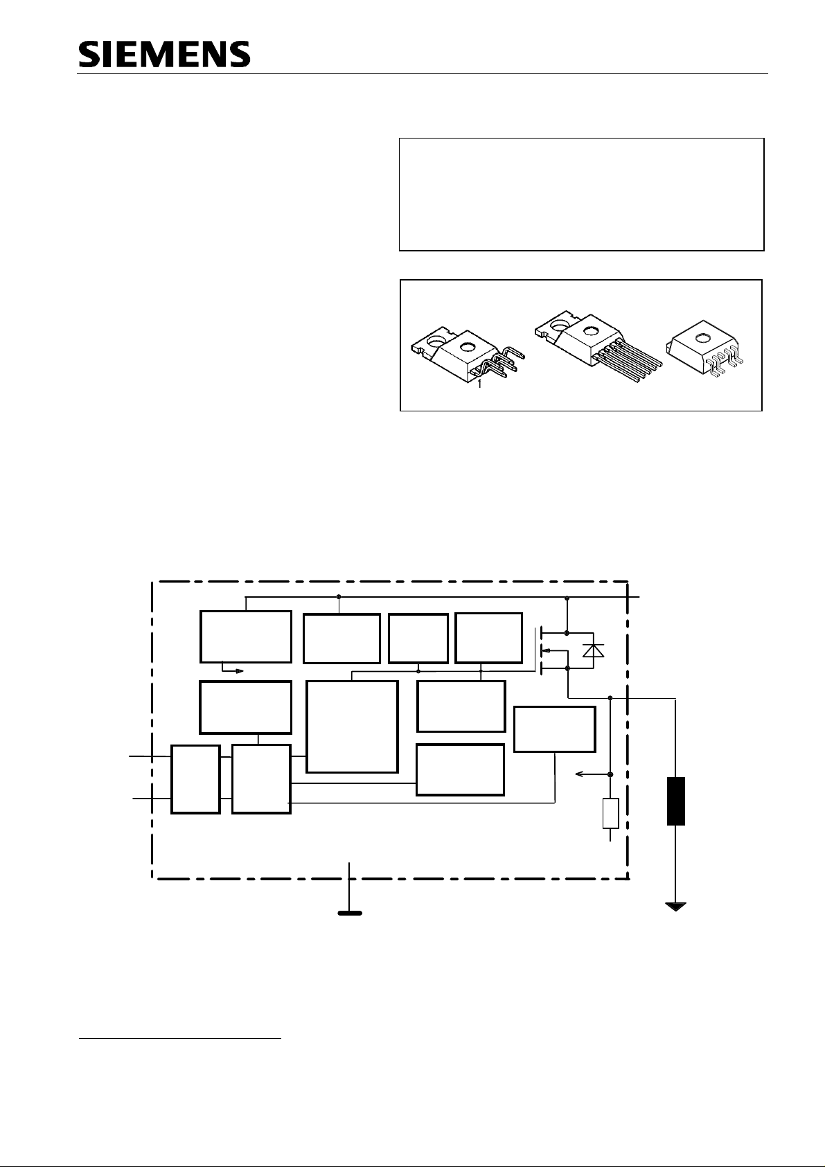
TO-220AB/5
5
Standard
Straight leads
V
bb(AZ
V
bb(on
R
ON
I
L(ISO
I
L(SCr
1
43 V
5.0 ... 34 V
60
7.0 A
16 A
5
1
SMD
Application
•
µC compatible power switch with diagnostic feedback for 12 V and 24 V DC grounded loads
•
All types of resistive, inductive and capacitve loads
•
Replaces electromechanical relays, fuses and discrete circuits
General Description
N channel vertical power FET with charge pump, ground referenced CMOS compatible input and diagnostic
feedback, monolithically integrated in Smart SIPMOS technology. Fully protected by embedded protection
functions.
m
Ω
5
+ V
bb
Voltage
source
V
Logic
Voltage
sensor
IN
2
ESD
4
ST
Logic
Overvoltage
protection
Charge pump
Level shifter
Rectifier
GND
Current
limit
unclamped
Open load
Short to Vbb
detection
Gate
protection
Limit for
ind. loads
Temperature
sensor
PROFET
R
O
GND
3
OUT
5
Load
1
Signal GND
Load GND
)
1
With external current limit (e.g. resistor R
=150 Ω) in GND connection, resistor in series with ST
GND
connection, reverse load current limited by connected load.
Semiconductor Group 1 12.96
Page 2
BTS 426 L1
j,
)
)
Pin Symbol Function
1 GND - Logic ground
2 IN I Input, activates the power switch in case of logical high signal
3Vbb+ Positive power supply voltage,
the tab is shorted to this pin
4 ST S Diagnostic feedback, low on failure
5 OUT
O Output to the load
(Load, L)
at
T
= 25 °C unless otherwise specified
Maximum Ratings
j
Parameter Symbol Values Unit
Supply voltage (overvoltage protection see page 3)
Supply voltage for full short circuit protection
T
=-40 ...+150°C
j Start
)
Load dump protection
)
3
R
= 2 Ω,
I
R
= 1.7 Ω,
L
2
V
LoadDump
t
= 200 ms, IN= low or high
d
=
U
+
V
A
,
s
U
= 13.5 V
A
Load current (Short circuit current, see page 4)
Operating temperature range
Storage temperature range
Power dissipation (DC), TC ≤ 25 °C
V
bb
V
bb
V
Load dump
I
L
T
j
T
stg
P
tot
43 V
34 V
)
4
60 V
self-limited A
-40 ...+150
°C
-55 ...+150
75 W
Inductive load switch-off energy dissipation, single pulse
V
= 12V,
Electrostatic discharge capability (ESD
(Human Body Model
acc. MIL-STD883D, method 3015.7 and ESD assn. std. S5.1-1993
Input voltage (DC)
Current through input pin (DC)
Current through status pin (DC)
see internal circuit diagrams page 6
T
= 150°C,
start
T
= 150°C const.
C
I
= 7.0 A, Z
L
= 24 mH, 0 Ω:
L
all other pins:
IN:
E
V
V
I
I
AS
ESD
IN
IN
ST
0.74 J
1.0
kV
2.0
-10 ... +16 V
±2.0
mA
±5.0
Thermal Characteristics
Parameter and Conditions Symbol Values Unit
min typ max
Thermal resistance chip - case:
junction - ambient (free air):
R
R
thJC
thJA
--
----1.67
--
SMD version, device on PCB5):34
)
2
Supply voltages higher than V
150 Ω resistor in the GND connection and a 15 kΩ resistor in series with the status pin. A resistor for the
protection of the input is integrated.
3)
R
= internal resistance of the load dump test pulse generator
I
4)
V
Load dump
)
5
Device on 50mm*50mm*1.5mm epoxy PCB FR4 with 6cm
connection. PCB is vertical without blown air.
is setup without the DUT connected to the generator per ISO 7637-1 and DIN 40839
require an external current limit for the GND and status pins, e.g. with a
bb(AZ)
2
(one layer, 70µm thick) copper area for V
Semiconductor Group 2
K/W
75
bb
Page 3
BTS 426 L1
)
j
)
Electrical Characteristics
Parameter and Conditions Symbol Values Unit
T
at
= 25 °C,
j
Load Switching Capabilities and Characteristics
On-state resistance (pin 3 to 5)
I
= 2 A
L
Nominal load current, ISO Norm (pin 3 to 5
V
= 0.5 V,
ON
Output current (pin 5) while GND disconnected or
GND pulled up,
page 7
Turn-on time IN to 90%
Turn-off time IN to 10%
R
= 12 Ω
L
Slew rate on
10 to 30%
Slew rate off
70 to 40%
V
= 12 V unless otherwise specified
bb
T
= 85 °C
C
V
=30 V,
bb
T
=-40...+150°C
,
j
V
V
OUT
OUT
R
,
R
,
= 12 Ω
L
= 12 Ω
L
V
= 0, see diagram
IN
T
=-40...+150°C
,
j
T
=-40...+150°C
,
j
T
=25 °C:
j
T
=150 °C:
j
V
V
OUT
OUT
:
:
R
I
I
t
t
dV /dt
-dV/dt
ON
L(ISO)
L(GNDhigh)
on
off
on
off
min typ max
-- 50
100
60
120
mΩ
5.8 7.0
-- A
-- -- 10 mA
80
80
200
230
400
450
0.1 -- 1 V/µs
0.1 -- 1 V/µs
µs
Operating Parameters
)
Operating voltage
6
Undervoltage shutdown
Undervoltage restart
T
j
T
j
T
Undervoltage restart of charge pump
see diagram page 12
T
j
Undervoltage hysteresis
V
∆
bb(under)
Overvoltage shutdown
Overvoltage restart
Overvoltage hysteresis
Overvoltage protection
I
=40 mA
bb
=
V
bb(u rst)
-
V
bb(under)
)
7
T
j
T
j
T
j
T
j
Standby current (pin 3)
V
=0
IN
Leakage output current (included in
IN
V
=0
=-40...+150°C:
=-40...+150°C:
=-40...+25°C:
T
=+150°C:
j
=-40...+150°C:
=-40...+150°C:
=-40...+150°C:
=-40...+150°C: ∆
=-40...+150°C:
T
=-40...+25°C
j
T
= 150°C:
j
I
)
bb(off
:
V
bb(on)
V
bb(under)
V
bb(u rst)
V
bb(ucp)
V
∆
bb(under)
V
bb(over)
V
bb(o rst)
V
bb(over)
V
bb(AZ)
I
bb(off)
I
L(off)
5.0 -- 34 V
3.5 -- 5.0 V
-- -- 5.0
V
7.0
-- 5.6 7.0 V
-- 0.2 -- V
34 -- 43 V
33 -- -- V
-- 0.5 -- V
42 47 -- V
--
--
10
12
25
28
µA
-- -- 12 µA
6)
At supply voltage increase up to
7)
See also
V
ON(CL)
in table of protection functions and circuit diagram page 7.
V
= 5.6 V typ without charge pump,
bb
Semiconductor Group 3
V
OUT
≈
V
- 2 V
bb
Page 4
BTS 426 L1
j
j
j
j
Parameter and Conditions Symbol Values Unit
at
T
= 25 °C,
j
V
= 12 V unless otherwise specified
bb
min typ max
Operating current (Pin 1)8),
=-40...+150°C
T
V
=5 V,
IN
Protection Functions
Initial peak short circuit current limit (pin 3 to 5)
=-40°C:
T
=25°C:
T
=+150°C:
j
T
Repetitive short circuit shutdown current limit
T
=
T
j
(see timing diagrams, page 10)
jt
Output clamp (inductive load switch off)
at
V
=
V
-
OUT
bb
V
ON(CL)
I
= 40 mA:
L
Thermal overload trip temperature
Thermal hysteresis
)
Reverse battery (pin 3 to 1)
Reverse battery voltage drop
= -4 A
I
L
9
(V
out
> V
bb
)
=150 °C:
T
j
Diagnostic Characteristics
Open load detection current
(on-condition)
Open load detection voltage
T
)
10
(off-condition)
T
=-40 °C
T
=25 ..150°C:
j
=-40..150°C:
j
Internal output pull down
(pin 5 to 1),
V
OUT
=5 V,
=-40..150°C
T
j
:
I
GND
I
L(SCp)
I
L(SCr)
V
ON(CL)
T
jt
∆T
jt
-
V
bb
-V
ON(rev)
I
L (OL)
V
OUT(OL)
R
O
-- 1.8 3.5 mA
21
15
11
32
25
17
43
35
24
A
-- 16 -- A
41 47 53 V
150 -- -- °C
-- 10 -- K
-- -- 32 V
20
10
--
610 --
--
850
--
750
mV
mA
234V
41030k
Ω
)
8
Add
)
9
Requires 150 Ω resistor in GND connection. The reverse load current through the intrinsic drain-source
diode has to be limited by the connected load. Note that the power dissipation is higher compared to normal
operating conditions due to the voltage drop across the intrinsic drain-source diode. The temperature
protection is not active during reverse current operation! Input and Status currents have to be limited (see
max. ratings page 2 and circuit page 7).
10)
External pull up resistor required for open load detection in off state.
, if
I
ST
> 0, add
I
ST
, if
V
>5.5 V
IN
I
IN
Semiconductor Group 4
Page 5

BTS 426 L1
Parameter and Conditions Symbol Values Unit
at
T
= 25 °C,
j
Input and Status Feedback
Input resistance
T
=-40..150°C, see circuit page 6
j
Input turn-on threshold voltage
Input turn-off threshold voltage
Input threshold hysteresis
Off state input current (pin 2),
T
=-40..+150°C
j
V
= 12 V unless otherwise specified
bb
)
11
V
= 0.4 V,
IN
T
=-40..+150°C:
j
T
=-40..+150°C:
j
R
I
V
IN(T+)
V
IN(T-)
∆
V
I
IN(off)
IN(T)
min typ max
2.5 3.5 6 k
1.7 -- 3.5 V
1.5 -- -- V
-- 0.5 -- V
1--50
µ
Ω
A
On state input current (pin 2),
T
=-40..+150°C
j
V
= 3.5 V,
IN
Delay time for status with open load after switch
off
(see timing diagrams, page 11
T
),
=-40..+150°C
j
Status invalid after positive input slope
(open load)
T
=-40 ... +150°C:
j
Status output (open drain)
Zener limit voltage
ST low voltage
T
=-40...+150°C,
j
T
=-40...+25°C,
j
T
= +150°C,
j
I
= +1.6 mA:
ST
I
= +1.6 mA:
ST
I
= +1.6 mA:
ST
I
IN(on)
t
d(ST OL4)
t
d(ST)
V
ST(high)
V
ST(low)
20 50 90
100 520 1000
-- 250 600
5.4
--
--
6.1
--
--
0.4
0.6
µ
A
µ
s
µ
s
--
V
11)
If a ground resistor R
is used, add the voltage drop across this resistor.
GND
Semiconductor Group 5
Page 6

BTS 426 L1
Truth Table
Input- Output Status
level level 425 L1
426 L1
Normal
operation
Open load L
Short circuit
to V
bb
Overtemperature
Undervoltage
Overvoltage L
L = "Low" Level X = don't care Z = high impedance, potential depends on external circuit
H = "High" Level Status signal after the time delay shown in the diagrams (see fig 5. page 11...12)
L
H
H
L
H
L
H
L
H
H
12
L
H
)
H
H
H
L
L
L
L
L
L
H (L
L
H (L
H
H
13
)
)
L
14
)
15
)
)
H
L
H
H
H
H
Terms
V
bb
Input circuit (ESD protection)
I
bb
R
GND
3
V
bb
PROFET
GND
1
I
GND
OUT
I
5
V
L
V
ON
OUT
ESD zener diodes are not to be used as voltage clamp
at DC conditions. Operation in this mode may result in
I
IN
IN
2
I
ST
ST
V
IN
4
V
ST
IN
a drift of the zener voltage (increase of up to 1 V).
R
I
ESD-ZD
I
GND
I
I
)
12
Power Transistor off, high impedance
)
13
with external resistor between pin 3 and pin 5
14)
An external short of output to Vbb, in the off state, causes an internal current from output to ground. If R
is used, an offset voltage at the GND and ST pins will occur and the V
)
15
Low resistance to
V
may be detected in ON-state by the no-load-detection
bb
signal may be errorious.
ST low
Semiconductor Group 6
GND
Page 7

Status output
BTS 426 L1
+5V
R
ST(ON)
GND
ST
ESD-
ZD
ESD-Zener diode: 6.1 V typ., max 5 mA;
R
ST(ON)
< 380 Ω at 1.6 mA, ESD zener diodes are not
to be used as voltage clamp at DC conditions.
Operation in this mode may result in a drift of the zener
voltage (increase of up to 1 V).
Inductive and overvoltage output clamp
+ V
bb
V
Z
V
ON
Open-load detection
ON-state diagnostic condition:
high
ON
Logic
unit
OFF-state diagnostic condition:
Open load
detection
V
R
<
ON
ON
V
> 3 V typ.; IN low
OUT
I
*
; IN
L(OL)
+ V
bb
V
ON
OUT
R
EXT
OUT
PROFET
V
clamped to 47 V typ.
ON
GND
Overvolt. and reverse batt. protection
+ V
V
R
GND
Z2
PROFET
GND
Signal GND
= 150 Ω,
R
IN
R
ST
V
= 6.2 V typ.,
Z1
R
= 15 kΩ,
ST
R
I
IN
ST
V
V
R
= 3.5 kΩ typ.
I
Logic
Z1
= 47 V typ.,
Z2
R
GND
OFF
V
OUT
Logic
unit
bb
Open load
detection
Signal GND
R
O
GND disconnect
3
V
IN
2
ST
4
V
V
IN
V
ST
bb
bb
PROFET
GND
1
V
GND
OUT
5
Semiconductor Group 7
Any kind of load. In case of Input=high is
Due to V
>0, no VST = low signal available.
GND
V
OUT
≈
V
V
-
IN
IN(T+)
.
Page 8

BTS 426 L1
GND disconnect with GND pull up
3
V
V
IN
bb
PROFET
GND
1
V
-
IN(T+)
OUT
5
V
GND
device stays off
V
bb
Any kind of load. If V
Due to V
V
IN
>0, no VST = low signal available.
GND
2
V
4
ST
GND
IN
ST
>
Vbb disconnect with energized inductive
load
3
high
IN
2
ST
4
V
bb
PROFET
GND
1
OUT
5
Inductive Load switch-off energy
dissipation
E
bb
E
AS
V
+ |V
E
bb
PROFET
GND
1
=
/
L
2
OUT(CL)
·L·
I
|)·
OUT
2
L
ON(CL)
> 0
L
ln
(1+
Z
L
·
Ω
L
{
R
L
iL(t) dt,
:
·
I
R
L
|V
OUT(CL)
L
IN
=
ST
Energy stored in load inductance:
While demagnetizing load inductance, the energy
dissipated in PROFET is
E
= Ebb + EL - ER= ∫ V
AS
with an approximate solution for R
·
I
L
L
=
·
(
V
bb
·
R
2
L
E
AS
E
E
|
E
)
Load
L
R
V
bb
Normal load current can be handled by the PROFET
itself.
Vbb disconnect with charged external
inductive load
S
3
high
V
bb
If other external inductive loads L are connected to the PROFET,
additional elements like D are necessary.
IN
2
ST
4
V
bb
PROFET
GND
1
OUT
5
D
Semiconductor Group 8
Page 9

BTS 426 L1
Maximum allowable load inductance for
a single switch off
L = f (I
V
=
bb
L
[mH]
10000
1000
100
);
L
12 V,
10
T
j,start
R
L
=
150°C,
=
Ω
0
T
150°C const.,
=
C
Transient thermal impedance chip ambient air
= f(tp)Z
Z
thJA
100
10
1
0.1
1E-5 1E-4 1E-3 1E-2 1E-1 1E0 1E1 1E2 1E3
thJA
[K/W]
D=
0.5
0.2
0.1
0.05
0.02
0.01
0
1
2 7 12 17
Typ. transient thermal impedance chip case
Z
thJC
0.1
= f(tp)Z
10
1
thJC
[K/W]
D=
0.5
0.2
0.1
0.05
0.02
0.01
0
I
L
[A]
t
[s]
p
0.01
1E-5 1E-4 1E-3 1E-2 1E-1 1E0 1E1
t
[s]
p
Semiconductor Group 9
Page 10

Timing diagrams
BTS 426 L1
Figure 1a: V
turn on:
bb
IN
V
bb
V
OUT
ST open drain
proper turn on under all conditions
Figure 2a: Switching a lamp,
Figure 2b: Switching an inductive load
IN
t
ST
V
OUT
I
L
I
t
*) if the time constant of load is too large, open-load-status may
occur
L(OL)
d(ST)
*)
t
IN
ST
V
I
OUT
L
Figure 3a: Short circuit
shut down by overtempertature, reset by cooling
IN
I
L
I
L(SCp)
I
L(SCr)
t
ST
t
Semiconductor Group 10
Heating up may require several milliseconds, depending on
external conditions
Page 11

BTS 426 L1
Figure 4a: Overtemperature:
T
Reset if
T
<
j
jt
IN
ST
V
OUT
T
J
Figure 5b: Open load: detection in ON-state, open
load occurs in on-state
IN
t
d(ST OL1)
ST
V
OUT
I
normal
L
open
t
t
d(ST OL2)
normal
t
Figure 5a: Open load: detection in ON-state, turn
on/off to open load
IN
ST
t
d(ST)
t
d(ST OL4)
V
OUT
I
L
open
t
d(ST OL1)
= 20 µs typ., t
d(ST OL2)
= 10 µs typ
Figure 5c: Open load: detection in ON- and OFF-state
(with R
), turn on/off to open load
EXT
IN
ST
V
OUT
t
d(ST)
I
L
open
t
t
The status delay time t
the failure modes "open load" and "overtemperature".
d(ST OL4)
allows to ditinguish between
Semiconductor Group 11
Page 12

Figure 6a: Undervoltage:
BTS 426 L1
Figure 7a: Overvoltage:
IN
V
bb
V
bb(u cp)
V
bb(u rst)
V
OUT
V
bb(under)
ST open drain
Figure 6b: Undervoltage restart of charge pump
V
V
on
ON(CL)
IN
V
V
bb
V
OUT
ON(CL)
V
bb(over)
V
bb(o rst)
ST
t
t
V
off-state
V
bb(u rst)
V
bb(under)
charge pump starts at
V
bb(u cp)
V
bb(ucp)
on-state
=5.6 V typ.
bb(over)
V
bb(o rst)
off-state
V
bb
Semiconductor Group 12
Page 13

Package and Ordering Code
)
All dimensions in mm
BTS 426 L1
Standard TO-220AB/5
BTS426L1 Q67060-S6108-A2
TO-220AB/5, Option E3043
BTS426L1 E3043 Q67060-S6108-A3
Ordering code
Ordering code
SMD TO-220AB/5, Opt. E3062
BTS426L1 E3062A T&R: Q67060-S6108-A4
Ordering code
Changed since 04.96
Date Change
Dec
1996
t
d(ST OL4
to 800µs, typical from 400 to
320µ
E
AS
max reduced from 1500
s, min limit unchanged
maximum rating and diagram
added
Z
th specification added
Typ. reverse battery voltage drop V
ON(rev) added
Components used in life-support devices or systems must be
expressly authorised for such purpose!
of the Semiconductor Group of Siemens AG, may only be used in
life supporting devices or systems
approval of the Semiconductor Group of Siemens AG.
16)
A critical component is a component used in a life-support
device or system whose failure can reasonably be expected to
cause the failure of that life-support device or system, or to
affect its safety or effectiveness of that device or system.
17)
Life support devices or systems are intended (a) to be
implanted in the human body or (b) support and/or maintain
and sustain and/or protect human life. If they fail, it is
reasonably to assume that the health of the user or other
persons may be endangered.
Critical components
)
17
with the express written
16
)
Semiconductor Group 13
 Loading...