

Page 1

DISCRETE SEMICONDUCTORS
DATA SH EET
BFG97
NPN 5 GHz wideband transistor
Product specification
File under Discrete Semiconductors, SC14
September 1995
Page 2
Philips Semiconductors Product specification
NPN 5 GHz wideband transistor BFG97
DESCRIPTION
NPN planar epitaxial transistor
mounted in a plastic SOT223
envelope.
It features excellent output voltage
capabilities, and is primarily intended
for use in MATV applications.
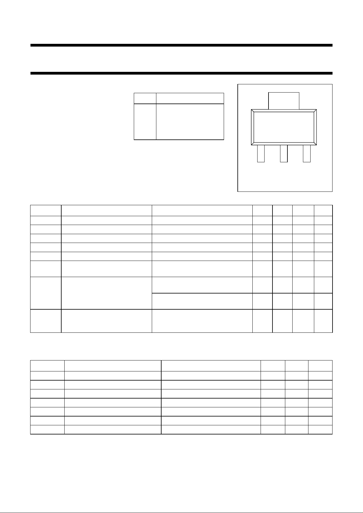
PINNING
PIN DESCRIPTION
1 emitter
2 base
3 emitter
4 collector
e
4
PNP complement is the BFG31.
123
Top view
MSB002 - 1
Fig.1 SOT223.
QUICK REFERENCE DATA
SYMBOL PARAMETER CONDITIONS MIN. TYP. MAX. UNIT
V
CBO
V
CEO
I
C
P
tot
h
FE
f
T
G
UM
V
o
collector-base voltage open emitter −−20 V
collector-emitter voltage open base −−15 V
DC collector current −−100 mA
total power dissipation up to Ts= 125 °C (note 1) −−1W
DC current gain IC= 70 mA; VCE= 10 V; Tj=25°C25 80 −
transition frequency IC= 70 mA; VCE= 10 V;
f = 500 MHz; T
amb
=25°C
maximum unilateral power gain IC= 70 mA; VCE= 10 V;
f = 500 MHz; T
= 70 mA; VCE= 10 V;
I
C
f = 800 MHz; T
amb
amb
=25°C
=25°C
output voltage IC= 70 mA; VCE= 10 V;
d
−60 dB; RL=75Ω;
im =
f
= 793.25 MHz; T
(p+q−r)
amb
=25°C
− 5.5 − GHz
− 16 − dB
− 12 − dB
− 700 − mV
LIMITING VALUES
In accordance with the Absolute Maximum System (IEC 134).
SYMBOL PARAMETER CONDITIONS MIN. MAX. UNIT
V
CBO
V
CEO
V
EBO
I
C
P
tot
T
stg
T
j
collector-base voltage open emitter − 20 V
collector-emitter voltage open base − 15 V
emitter-base voltage open collector − 3V
DC collector current − 100 mA
total power dissipation up to Ts= 125 °C (note 1) − 1W
storage temperature −65 150 °C
junction temperature − 175 °C
Note
is the temperature at the soldering point of the collector tab.
1. T
s
September 1995 2
Page 3
Philips Semiconductors Product specification
NPN 5 GHz wideband transistor BFG97
THERMAL RESISTANCE
SYMBOL PARAMETER CONDITIONS THERMAL RESISTANCE
R
th j-s
Note
1. T
is the temperature at the soldering point of the collector tab.
s
CHARACTERISTICS
=25°C unless otherwise specified.
T
j
SYMBOL PARAMETER CONDITIONS MIN. TYP. MAX. UNIT
I
CBO
h
FE
f
T
C
c
C
e
C
re
G
UM
V
o
d
2
thermal resistance from junction to
up to Ts= 125 °C (note 1) 50 K/W
soldering point
collector cut-off current IE= 0; VCB= 10 V −−100 nA
DC current gain IC= 70 mA; VCE= 10 V 25 80 −
transition frequency IC= 70 mA; VCE= 10 V;
f = 500 MHz; T
amb
=25°C
− 5.5 − GHz
collector capacitance IE=ie= 0; VCB= 10 V; f = 1 MHz − 1.5 − pF
emitter capacitance IC=ic= 0; VEB= 0.5 V; f = 1 MHz − 6.5 − pF
feedback capacitance IC= 0; VCE= 10 V; f = 1 MHz − 1 − pF
maximum unilateral power gain
(note 1)
IC= 70 mA; VCE= 10 V;
f = 500 MHz; T
I
= 70 mA; VCE= 10 V;
C
f = 800 MHz; T
amb
amb
=25°C
=25°C
− 16 − dB
− 12 − dB
output voltage note 2 − 750 − mV
note 3 − 700 − mV
second order intermodulation
distortion
note 4 −−56 − dB
note 5 −−53 − dB
Notes
1. G
2. d
is the maximum unilateral power gain, assuming S12is zero and
UM
G
UM
= −60 dB (DIN 45004B); IC= 70 mA; VCE= 10 V; RL=75Ω; T
im
--------------------------------------------------------------
10 log
1S
S
2
–
11
2
21
1S
–
Vp=Voat dim= −60 dB;
Vq=Vo−6 dB; fp= 445.25 MHz;
Vr=Vo−6 dB; fq= 453.25 MHz; fr= 455.25 MHz;
measured at f
= 443.25 MHz.
(p+q−r)
3. dim= −60 dB (DIN 45004B); IC= 70 mA; VCE= 10 V; RL=75Ω; T
Vp=Voat dim= −60 dB;
Vq=Vo−6 dB; fp= 795.25 MHz;
Vr=Vo−6 dB; fq= 803.25 MHz; fr= 805.25 MHz;
measured at f
4. IC= 70 mA; VCE= 10 V; RL=75Ω; T
Vp=Vq=Vo= 50 dBmV; f
5. IC= 70 mA; VCE= 10 V; RL=75Ω; T
Vp=Vq=Vo= 50 dBmV; f
= 793.25 MHz.
(p+q−r)
=25°C;
amb
= 450 MHz; fp= 50 MHz; fq= 400 MHz.
(p+q)
=25°C;
amb
= 810 MHz; fp= 250 MHz; fq= 560 MHz.
(p+q)
September 1995 3
22
amb
amb
dB.=
2
=25°C
=25°C
Page 4
Philips Semiconductors Product specification
NPN 5 GHz wideband transistor BFG97
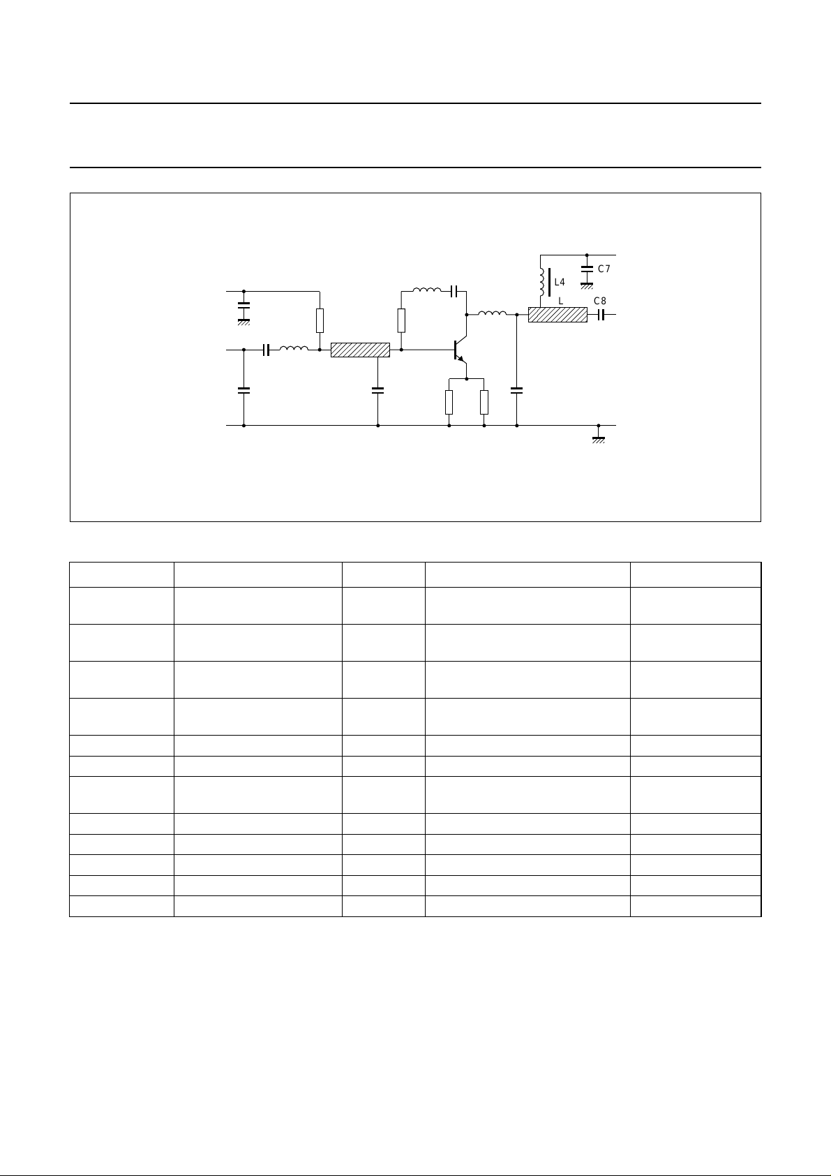
handbook, full pagewidth
V
BB
input
75 Ω
C3
C2
C4
L2
L5
R1
L1C1
L3
R2
DUT
C5
R3 R4
L4
C6
MBB807
V
CC
C7
C8L6
output
75 Ω
Fig.2 Intermodulation distortion and second order intermodulation distortion test circuit.
List of components (see test circuit)
DESIGNATION DESCRIPTION VALUE DIMENSIONS CATALOGUE NO.
C2, C3, C7, C8 multilayer ceramic
10 nF 2222 590 08627
capacitor
C1, C4, C6 multilayer ceramic
1.2 pF 2222 851 12128
capacitor
C5 (note 1) miniature ceramic plate
10 nF 2222 629 08103
capacitor
L1 (note 1) 0.5 turns 0.4 mm copper
int. dia. 3 mm
wire
L2 microstripline 75 Ω length 14 mm; width 2.5 mm
L3 microstripline 75 Ω length 8 mm; width 2.5 mm
L4, L5 (note 1) 1.5 turns 0.4 mm copper
wire
int. dia. 3 mm;
winding pitch 1 mm
L6 microstripline 75 Ω length 19 mm; width 2.5 mm
L7 Ferroxcube choke 5 µH 3122 108 20153
R1 metal film resistor 10 kΩ 2322 180 73103
R2 (note 1) metal film resistor 220 Ω 2322 180 73221
R3, R4 metal film resistor 30 Ω 2322 180 73309
Notes
The circuit has been built on a double copper-clad printed circuit board with PTFE dielectric (ε
thickness of copper sheet 2 × 35 µm.
1. Components C5, L1, L4, L5, and R2 are mounted on the underside of the PCB.
September 1995 4
= 2.2); thickness1⁄16 inch;
r
Page 5
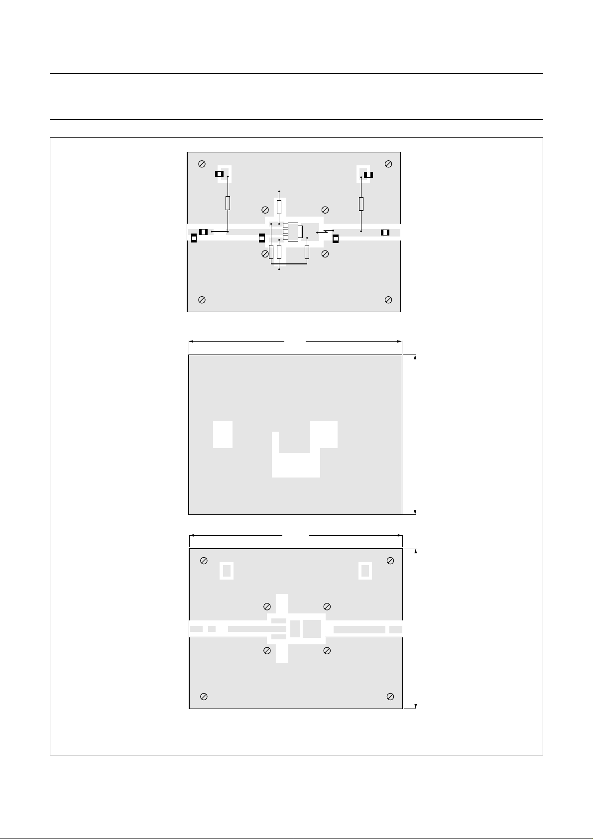
Philips Semiconductors Product specification
NPN 5 GHz wideband transistor BFG97
handbook, full pagewidth
handbook, full pagewidth
75
input
V
BB
C3
R1
C2
Ω
L1
L2
C1
R3
L3
C4
R4
R2
L4
80 mm
L5
C5
V
CC
C7
L7
C8
75
L6
C6
MEA971
output
60 mm
Ω
handbook, full pagewidth
mounting
screws
M 2.5 (8x)
80 mm
Fig.3 Intermodulation distortion and second order intermodulation distortion printed circuit board.
September 1995 5
MEA969
60 mm
MEA970
Page 6

Philips Semiconductors Product specification
NPN 5 GHz wideband transistor BFG97
1.2
handbook, halfpage
P
tot
(W)
1.0
0.8
0.6
0.4
0.2
0
0 50 100 200
150
T ( C)
Fig.4 Power derating curve.
MBB797
s
I (mA)
C
MBB774
120
handbook, halfpage
h
FE
80
40
0
o
0
VCE= 10 V; Tj=25°C.
40 120
80
Fig.5 DC current gain as a function of collector
current.
handbook, halfpage
3
C
re
(pF)
2
1
0
0
IE= 0; f= 1 MHz; Tj=25°C.
10 20
V (V)
MBB798
CE
Fig.6 Feedback capacitance as a function of
collector-emitter voltage.
September 1995 6
handbook, halfpage
8
f
T
(GHz)
6
4
2
0
04080
VCE= 10 V; f = 500 MHz; Tj=25°C.
I (mA)
C
Fig.7 Transition frequency as a function of
collector current.
MBB773
120
Page 7

Philips Semiconductors Product specification
NPN 5 GHz wideband transistor BFG97
45
handbook, halfpage
d
im
(dB)
50
55
60
65
70
20 120
VCE= 10 V; Vo= 750 mV; f
=25°C.
T
amb
40 60 80 100
= 443.25 MHz;
(p+q−r)
MBB799
I (mA)
C
Fig.8 Intermodulation distortion as a function of
collector current.
45
handbook, halfpage
d
im
(dB)
50
55
60
65
70
20 120
VCE= 10 V; Vo= 700 mV; f
=25°C.
T
amb
40 60 80 100
= 793.25 MHz;
(p+q−r)
MBB796
I (mA)
C
Fig.9 Intermodulation distortion as a function of
collector current.
45
handbook, halfpage
d
2
(dB)
50
55
60
65
70
20 120
VCE= 10 V; Vo= 50 dBmV; f
=25°C.
T
amb
40 60 80 100
(p+q)
= 450 MHz;
MBB800
I (mA)
C
Fig.10 Second order intermodulation distortion as
a function of collector current.
45
handbook, halfpage
d
2
(dB)
50
55
60
65
70
20 120
VCE= 10 V; Vo= 50 dBmV; f
=25°C.
T
amb
40 60 80 100
(p+q)
= 810 MHz;
MBB801
I (mA)
C
Fig.11 Second order intermodulation distortion as
a function of collector current.
September 1995 7
Page 8

Philips Semiconductors Product specification
NPN 5 GHz wideband transistor BFG97
L
L
0.75
P
MEA963
OUT
60
handbook, halfpage
Z
L
(Ω)
50
40
30
20
10
0
–10
–20
0 0.25
VCE= 6 V; f = 900 MHz.
R
X
0.50
Fig.12 Load impedance as a function of output
power.
(W)
0.75
R
X
P
MEA964
L
L
OUT
(W)
1
60
handbook, halfpage
Z
L
(Ω)
50
40
30
20
10
0
–10
1
0 0.25
VCE= 7.5 V; f = 900 MHz.
0.50
Fig.13 Load impedance as a function of output
power.
0.75
P
MEA965
OUT
60
handbook, halfpage
Z
L
(Ω)
50
40
30
20
10
0
–10
0 0.25
VCE= 10 V; f = 900 MHz.
0.50
Fig.14 Load impedance as a function of output
power.
R
X
(W)
L
L
1
September 1995 8
Page 9

Philips Semiconductors Product specification
NPN 5 GHz wideband transistor BFG97
i
i
0.75
P
MEA957
OUT
20
handbook, halfpage
Z
i
(Ω)
15
10
5
0
–5
0 0.25
VCE= 6 V; f = 900 MHz.
x
r
0.50
Fig.15 Input impedance as a function of output
power.
(W)
0.75
P
r
x
OUT
MEA958
i
i
(W)
1
20
handbook, halfpage
Z
i
(Ω)
15
10
5
0
–5
1
0 0.25
VCE= 7.5 V; f = 900 MHz.
0.50
Fig.16 Input impedance as a function of output
power.
0.75
P
MEA959
OUT
20
handbook, halfpage
Z
i
(Ω)
15
10
5
0
5
–10
0 0.25
VCE= 10 V; f = 900 MHz.
0.50
Fig.17 Input impedance as a function of output
power.
(W)
r
i
x
i
1
September 1995 9
Page 10

Philips Semiconductors Product specification
NPN 5 GHz wideband transistor BFG97
80
handbook, halfpage
η
(%)
70
V =CE6 V
60
7.5 V
50
40
0 0.5 1.5
f = 900 MHz.
10 V
1
P
OUT
Fig.18 Efficiency as a function of output power.
MEA961
(W)
1.5
handbook, halfpage
P
OUT
(W)
1
0.5
0
0 100 300
f = 900 MHz.
200
MEA962
V =
CE
10 V
7.5 V
PIN(mW)
6 V
Fig.19 Output power as a function of input power.
V =
CE
10 V
P
OUT
MEA960
(W)
10
handbook, halfpage
G
p
(dB)
8
6
4
2
0
0 0.5 1.5
f = 900 MHz.
7.5 V
6 V
1
Fig.20 Power gain as a function of output power.
50
handbook, halfpage
G
UM
(dB)
40
30
20
10
0
10
IC= 70 mA; VCE= 10 V; T
2
10
=25°C.
amb
3
10
f (MHz)
Fig.21 Maximum unilateral power gain as a
function of frequency.
MBB802
4
10
September 1995 10
Page 11
Philips Semiconductors Product specification
NPN 5 GHz wideband transistor BFG97
50
handbook, full pagewidth
25
40 MHz
100
IC= 70 mA; VCE= 10 V; T
Zo=50Ω.
handbook, full pagewidth
amb
10
+ j
0
– j
10
=25°C.
10 25 50 100 250
2 GHz
25
50
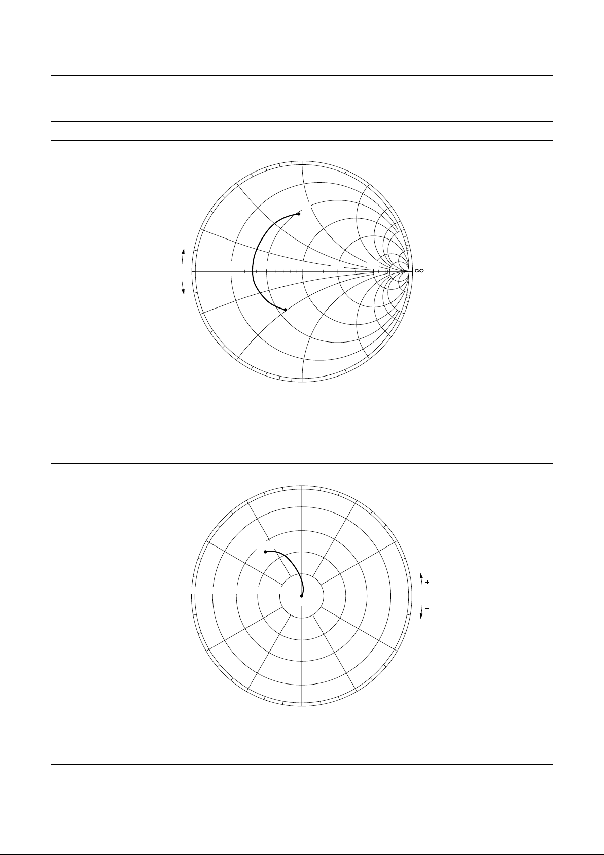
Fig.22 Common emitter input reflection coefficient (S11).
o
90
120
o
o
60
250
250
100
MBB803
o
IC= 70 mA; VCE= 10 V; T
amb
180
=25°C.
150
80 40100 60 20
o
o
150
120
2 GHz
40 MHz
o
90
Fig.23 Common emitter forward transmission coefficient (S21).
September 1995 11
o
30
ϕ
o
0
ϕ
o
30
o
60
o
MBB806
Page 12

Philips Semiconductors Product specification
NPN 5 GHz wideband transistor BFG97
o
90
handbook, full pagewidth
120
o
o
60
IC= 70 mA; VCE= 10 V; T
handbook, full pagewidth
amb
180
=25°C.
o
150
0.4 0.20.5 0.3 0.1
o
o
150
120
40 MHz
o
2 GHz
o
60
o
90
Fig.24 Common emitter reverse transmission coefficient (S12).
50
25
100
o
30
o
30
MBB805
ϕ
o
0
ϕ
10
2 GHz
50
IC= 70 mA; VCE= 10 V; T
=50Ω.
Z
o
amb
+ j
– j
=25°C.
0
10
10 25 50 100 250
25
Fig.25 Common emitter output reflection coefficient (S22).
September 1995 12
250
250
40 MHz
100
MBB804
Page 13
Philips Semiconductors Product specification
NPN 5 GHz wideband transistor BFG97
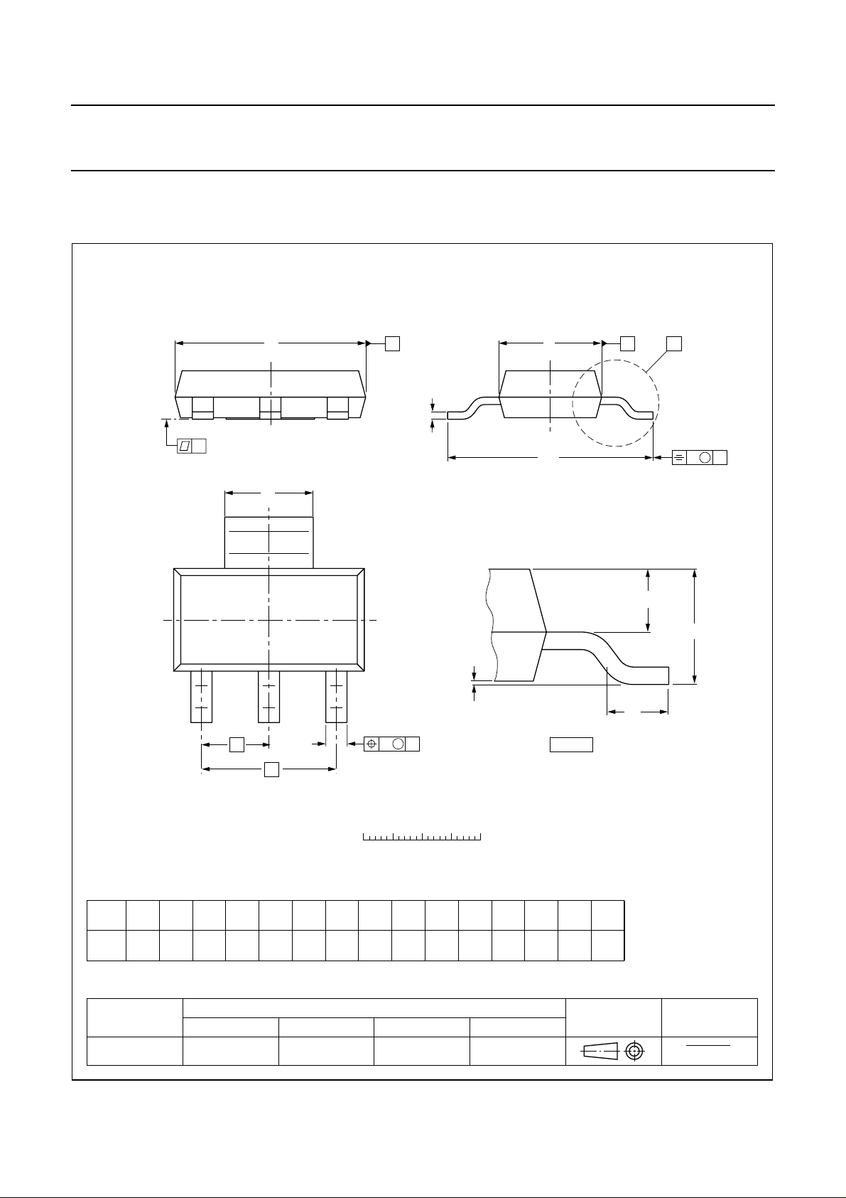
PACKAGE OUTLINE
Plastic surface mounted package; collector pad for good heat transfer; 4 leads SOT223
D
c
y
b
1
4
132
e
1
b
p
e
w M
B
E
H
E
A
1
detail X
AB
L
X
v M
A
Q
A
p
0 2 4 mm
scale
DIMENSIONS (mm are the original dimensions)
mm
OUTLINE
VERSION
SOT223
1.8
1.5
A
0.10
0.01
p
0.80
0.60
IEC JEDEC EIAJ
3.1
2.9
b
1
cD
0.32
6.7
0.22
6.3
e
E
3.7
4.6
3.3
REFERENCES
e1HELpQywv
2.3
UNIT A1b
September 1995 13
7.3
6.7
1.1
0.7
0.95
0.85
0.1 0.10.2
EUROPEAN
PROJECTION
ISSUE DATE
96-11-11
97-02-28
Page 14

Philips Semiconductors Product specification
NPN 5 GHz wideband transistor BFG97
DEFINITIONS
Data Sheet Status
Objective specification This data sheet contains target or goal specifications for product development.
Preliminary specification This data sheet contains preliminary data; supplementary data may be published later.
Product specification This data sheet contains final product specifications.
Limiting values
Limiting values given are in accordance with the Absolute Maximum Rating System (IEC 134). Stress above one or
more of the limiting values may cause permanent damage to the device. These are stress ratings only and operation
of the device at these or at any other conditions above those given in the Characteristics sections of the specification
is not implied. Exposure to limiting values for extended periods may affect device reliability.
Application information
Where application information is given, it is advisory and does not form part of the specification.
LIFE SUPPORT APPLICATIONS
These products are not designed for use in life support appliances, devices, or systems where malfunction of these
products can reasonably be expected to result in personal injury. Philips customers using or selling these products for
use in such applications do so at their own risk and agree to fully indemnify Philips for any damages resulting from such
improper use or sale.
September 1995 14
 Loading...