


DISCRETE SEMICONDUCTORS
DATA SH EET
BFG25A/X
NPN 5 GHz wideband transistor
Product specification
Supersedes data of September 1995
File under Discrete Semiconductors, SC14
1997 Oct 29

Philips Semiconductors Product specification
NPN 5 GHz wideband transistor BFG25A/X
FEATURES
• Low current consumption
(100 µA to 1 mA)
• Low noise figure
DESCRIPTION
NPN silicon wideband transistor in a
four-lead dual emitter SOT143B
plastic package (cross emitter).
handbook, 2 columns
34
• Gold metallization ensures
excellent reliability.
APPLICATIONS
• RF low power amplifiers, such as
pocket telephones, paging
systems, with signal frequencies
up to 2 GHz.
PINNING
PIN DESCRIPTION
1 collector
2 emitter
3 base
4 emitter
12
Top view
Marking code: V11.
MSB014
Fig.1 SOT143B.
QUICK REFERENCE DATA
SYMBOL PARAMETER CONDITIONS MIN. TYP. MAX. UNIT
V
CBO
V
CEO
I
C
P
tot
h
FE
f
T
G
UM
F noise figure I
collector-base voltage −−8V
collector-emitter voltage −−5V
collector current (DC) −−6.5 mA
total power dissipation Ts≤ 165 °C −−32 mW
DC current gain IC= 0.5 mA; VCE=1V 5080200
transition frequency IC= 1 mA; VCE=1V;
f = 500 MHz; T
amb
=25°C
maximum unilateral power gain IC= 0.5 mA; VCE=1V;
f = 1 GHz; T
= 0.5 mA; VCE=1V;
C
f = 1 GHz; Γ = Γ
I
= 1 mA; VCE= 1 V; f = 1 GHz;
C
Γ = Γ
opt
; T
amb
amb
=25°C
; T
opt
=25°C
amb
=25°C
3.5 5 − GHz
− 18 − dB
− 1.8 − dB
− 2 − dB
1997 Oct 29 2
Philips Semiconductors Product specification
NPN 5 GHz wideband transistor BFG25A/X
LIMITING VALUES
In accordance with the Absolute Maximum Rating System (IEC 134).
SYMBOL PARAMETER CONDITIONS MIN. MAX. UNIT
V
CBO
V
CEO
V
EBO
I
C
P
tot
T
stg
T
j
Note
1. T
s
THERMAL CHARACTERISTICS
collector-base voltage open emitter − 8V
collector-emitter voltage open base − 5V
emitter-base voltage open collector − 2V
collector current (DC) − 6.5 mA
total power dissipation Ts≤ 165 °C; note 1 − 32 mW
storage temperature −65 150 °C
junction temperature − 175 °C
is the temperature at the soldering point of the collector pin.
SYMBOL PARAMETER CONDITIONS VALUE UNIT
R
th j-s
thermal resistance from junction to soldering point note 1 320 K/W
Note
1. T
is the temperature at the soldering point of the collector pin.
s
CHARACTERISTICS
=25°C unless otherwise specified.
T
j
SYMBOL P ARAMETER CONDITIONS MIN. TYP. MAX. UNIT
I
CBO
h
FE
C
re
f
T
G
UM
F noise figure I
Note
1. G
collector leakage current IE= 0; VCB=5V −−50 µA
DC current gain IC= 0.5 mA; VCE=1V 5080200
feedback capacitance IC=ic= 0; VCB= 1 V; f = 1 MHz − 0.21 0.3 pF
transition frequency IC= 1 mA; VCE=1V;
T
=25°C; f = 500 MHz
amb
maximum unilateral power gain
(note 1)
is the maximum unilateral power gain, assuming S12 is zero and
UM
IC= 0.5 mA; VCE=1V;
f = 1 GHz; T
= 0.5 mA; VCE= 1 V; f = 1 GHz;
C
Γ = Γ
I
Γ = Γ
; T
opt
= 1 mA; VCE= 1 V; f = 1 GHz;
C
; T
opt
amb
amb
amb
=25°C
=25°C
=25°C
G
UM
3.5 5 − GHz
− 18 − dB
− 1.8 − dB
− 2 − dB
10 log
--------------------------------------------------------------
1
S
–
11
2
S
21
2
1
–
dB=
2
S
22
1997 Oct 29 3
Philips Semiconductors Product specification
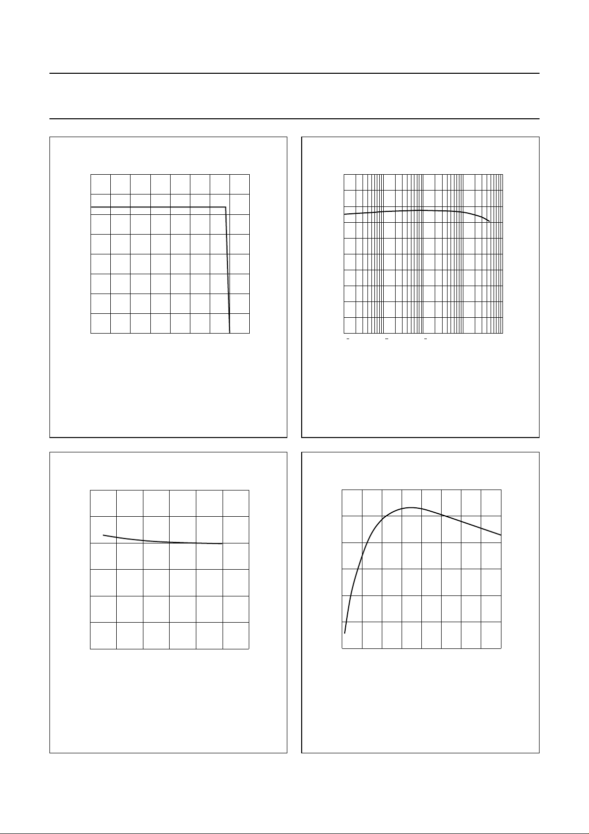
NPN 5 GHz wideband transistor BFG25A/X
40
handbook, halfpage
P
tot
(mW)
30
20
10
0
0 50 100 200
150
Fig.2 Power derating curve.
MRC038 - 1
Ts (oC)
100
handbook, halfpage
h
FE
80
60
40
20
0
10
VCE=1V.
3
2
10
1
110
I (mA)
C
Fig.3 DC current gain as a function of collector
current; typical values.
MCD138
10
0.3
handbook, halfpage
C
re
(pF)
0.2
0.1
0
0
IC=ic= 0; f= 1 MHz.
246
MCD139
V (V)
CB
Fig.4 Feedback capacitance as a function of
collector-base voltage; typical values.
1997 Oct 29 4
handbook, halfpage
6
f
T
(GHz)
4
2
0
0
VCE= 1 V; f = 500 MHz; T
12 4
amb
=25°C.
Fig.5 Transition frequency as a function of
collector current; typical values.
3
MCD140
I (mA)
C

Philips Semiconductors Product specification
NPN 5 GHz wideband transistor BFG25A/X
30
handbook, halfpage
G
gain
(dB)
20
10
0
VCE= 1 V; f = 500 MHz.
GUM = maximum unilateral power gain;
MSG = maximum stable gain.
0.5 1.5 2.0
0 1.0 2.5
UM
MSG
Fig.6 Gain as a function of collector current;
typical values.
MCD141
I (mA)
C
20
handbook, halfpage
gain
(dB)
15
10
5
0
0 1.0 2.5
0.5 1.5 2.0
VCE= 1 V; f = 1 GHz.
GUM = maximum unilateral power gain;
MSG = maximum stable gain.
G
UM
MSG
Fig.7 Gain as a function of collector current;
typical values.
MCD142
I (mA)
C
3
f (MHz)
MCD143
4
10
50
handbook, halfpage
gain
(dB)
40
30
20
10
0
10 10
IC= 0.5 mA; VCE=1V.
GUM = maximum unilateral power gain;
MSG = maximum stable gain.
G
UM
MSG
2
10
Fig.8 Gain as a function of frequency;
typical values.
1997 Oct 29 5
50
handbook, halfpage
gain
(dB)
40
30
20
10
0
10 10
IC= 1 mA; VCE=1V.
GUM = maximum unilateral power gain;
MSG = maximum stable gain.
G
UM
MSG
2
Fig.9 Gain as a function of frequency;
typical values.
MCD144
3
10
f (MHz)
4
10

Philips Semiconductors Product specification
NPN 5 GHz wideband transistor BFG25A/X
handbook, halfpage
4
F
(dB)
3
2
1
0
−1
10
VCE=1V.
f = 2 GHz
1 GHz
500 MHz
110
IC (mA)
Fig.10 Minimum noise figure as a function of
collector current; typical values.
MCD145
handbook, halfpage
4
F
(dB)
3
2
1
0
10
VCE=1V.
IC = 2 mA
1 mA
0.5 mA
2
3
10
f (MHz)
Fig.11 Minimum noise figure as a function of
frequency; typical values.
MCD146
4
10
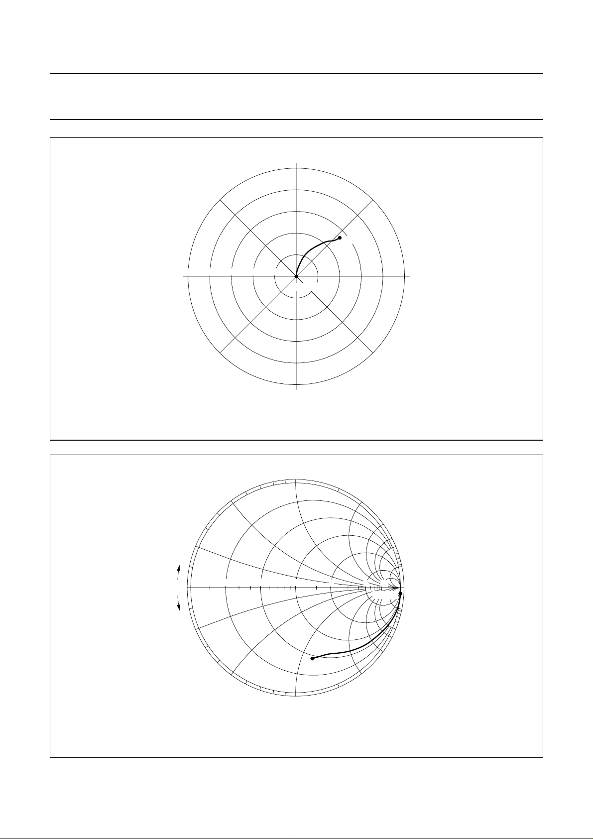
handbook, full pagewidth
0.5
0.2
+
j
0
– j
0.2
IC= 1 mA; VCE= 1 V; f = 500 MHz; ZO=50Ω;Maximum stable gain =15.6 dB; F
unstable region
0.5
MSG
15.6 dB
14 dB
12 dB
Fig.12 Common emitter noise figure circles; typical values.
1
2
6 dB
4 dB
2.5 dB
101520.50.2
*
2
1
= 1.9 dB; Γ
min
= 0.85, 5°; Rn/50 = 2.4.
opt
5
5
MCD147
stability
circle
10
∞
F = 1.9 dB
10
OPT
min
1997 Oct 29 6

Philips Semiconductors Product specification
NPN 5 GHz wideband transistor BFG25A/X
handbook, full pagewidth
0.5
0.2
+
j
0
– j
0.2
IC= 1 mA; VCE= 1 V; f = 1000 MHz; ZO=50Ω;Maximum stable gain =12.4 dB; F
unstable region
0.5
0.5 10.2 1052
MSG
12.4 dB
11 dB
9 dB
Fig.13 Common emitter noise figure circles; typical values.
1
2
stability
6 dB
4 dB
3 dB
*
circle
5
10
OPT
F = 2 dB
min
∞
10
5
2
1
= 2 dB; Γ
min
MCD148
= 0.78, 14°; Rn/50 = 2.6.
opt
handbook, full pagewidth
0.5
unstable region
0.2
+ j
0
0
– j
0.2
0.5
IC= 1 mA; VCE= 1 V; f = 2000 MHz; ZO=50Ω; Maximum stable gain= 8.9dB; F
0.5 10.2 1052
MSG
9 dB
7.5 dB
6 dB
Fig.14 Common emitter noise figure circles; typical values.
1
6 dB
10.2 10520.5
1
4 dB
3 dB
= 2.4 dB; Γ
min
stability
circle
2
F = 2.4 dB
*
2
MCD149
= 0.72, 38°; Rn/50 = 1.9.
opt
OPT
min
5
10
∞
10
5
1997 Oct 29 7

Philips Semiconductors Product specification
NPN 5 GHz wideband transistor BFG25A/X
handbook, full pagewidth
IC= 1 mA; VCE= 1 V; Zo=50Ω.
1
0.5
0.2
+ j
0
– j
0.2
0.5
0.5 10.2 1052
3 GHz
1
2
40 MHz
2
5
10
∞
10
5
MCD150
Fig.15 Common emitter input reflection coefficient (S11); typical values.
handbook, full pagewidth
IC= 1 mA; VCE=1V.
o
90
o
45
o
0
54321
_
o
45
MCD151
180
o
135
3 GHz
o
40 MHz
_
o
135
_
o
90
Fig.16 Common emitter forward transmission coefficient (S21); typical values.
1997 Oct 29 8
Philips Semiconductors Product specification
NPN 5 GHz wideband transistor BFG25A/X
o
90
handbook, full pagewidth
IC= 1 mA; VCE=1V.
handbook, full pagewidth
180
o
135
3 GHz
o
_
o
135
0.10.20.30.40.5
40 MHz
_90o
_
45
45
MCD153
o
o
0
o
Fig.17 Common emitter reverse transmission coefficient (S12); typical values.
1
0.5
2
0.2
+ j
0
– j
0.2
0.5
IC= 1 mA; VCE= 1 V; Zo=50Ω.
0.5 10.2 1052
Fig.18 Common emitter output reflection coefficient (S22); typical values.
1997 Oct 29 9
1
3 GHz
2
40 MHz
MCD152
5
10
∞
10
5
Philips Semiconductors Product specification
NPN 5 GHz wideband transistor BFG25A/X
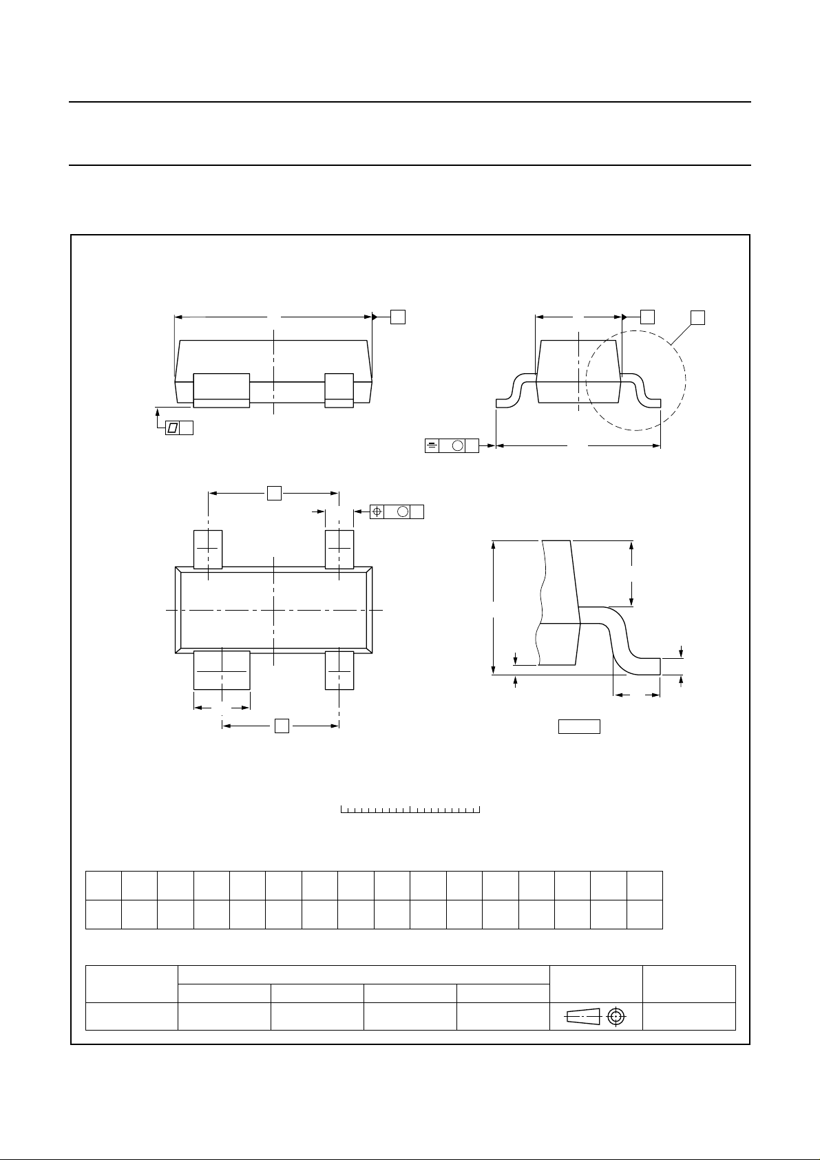
PACKAGE OUTLINE
Plastic surface mounted package; 4 leads SOT143B
D
y
e
b
p
B
w M
E
v M
A
B
H
E
A
X
34
Q
A
A
1
21
b
1
e
1
detail X
L
c
p
0 1 2 mm
scale
DIMENSIONS (mm are the original dimensions)
A
UNIT
mm
1.1
0.9
OUTLINE
VERSION
SOT143B
1
A
max
0.1
b
c
D
3.0
1.4
2.8
1.2
REFERENCES
E
b
0.48
0.38
1
p
0.88
0.15
0.78
0.09
IEC JEDEC EIAJ
e
1.9
1997 Oct 29 10
e
1.7
H
L
E
1
2.5
2.1
0.45
0.15
p
0.55
0.45
EUROPEAN
PROJECTION
ywvQ
0.1 0.10.2
ISSUE DATE
97-02-28

Philips Semiconductors Product specification
NPN 5 GHz wideband transistor BFG25A/X
DEFINITIONS
Data sheet status
Objective specification This data sheet contains target or goal specifications for product development.
Preliminary specification This data sheet contains preliminary data; supplementary data may be published later.
Product specification This data sheet contains final product specifications.
Limiting values
Limiting values given are in accordance with the Absolute Maximum Rating System (IEC 134). Stress above one or
more of the limiting values may cause permanent damage to the device. These are stress ratings only and operation
of the device at these or at any other conditions above those given in the Characteristics sections of the specification
is not implied. Exposure to limiting values for extended periods may affect device reliability.
Application information
Where application information is given, it is advisory and does not form part of the specification.
LIFE SUPPORT APPLICATIONS
These products are not designed for use in life support appliances, devices, or systems where malfunction of these
products can reasonably be expected to result in personal injury. Philips customers using or selling these products for
use in such applications do so at their own risk and agree to fully indemnify Philips for any damages resulting from such
improper use or sale.
1997 Oct 29 11

Philips Semiconductors – a worldwide company
Argentina: see South America
Australia: 34 Waterloo Road, NORTH RYDE, NSW 2113,
Tel. +61 2 9805 4455, Fax. +61 2 9805 4466
Austria: Computerstr. 6, A-1101 WIEN, P.O. Box 213, Tel. +43 160 1010,
Fax. +43 160 101 1210
Belarus: Hotel Minsk Business Center, Bld. 3, r. 1211, Volodarski Str. 6,
220050 MINSK, Tel. +375 172 200 733, Fax. +375 172 200 773
Belgium: see The Netherlands
Brazil: see South America
Bulgaria: Philips Bulgaria Ltd., Energoproject, 15th floor,
51 James Bourchier Blvd., 1407 SOFIA,
Tel. +359 2 689 211, Fax. +359 2 689 102
Canada: PHILIPS SEMICONDUCTORS/COMPONENTS,
Tel. +1 800 234 7381
China/Hong Kong: 501 Hong Kong Industrial Technology Centre,
72 Tat Chee Avenue, Kowloon Tong, HONG KONG,
Tel. +852 2319 7888, Fax. +852 2319 7700
Colombia: see South America
Czech Republic: see Austria
Denmark: Prags Boulevard 80, PB 1919, DK-2300 COPENHAGEN S,
Tel. +45 32 88 2636, Fax. +45 31 57 0044
Finland: Sinikalliontie 3, FIN-02630 ESPOO,
Tel. +358 9 615800, Fax. +358 9 61580920
France: 4 Rue du Port-aux-Vins, BP317, 92156 SURESNES Cedex,
Tel. +33 1 40 99 6161, Fax. +33 1 40 99 6427
Germany: Hammerbrookstraße 69, D-20097 HAMBURG,
Tel. +49 40 23 53 60, Fax. +49 40 23 536 300
Greece: No. 15, 25th March Street, GR 17778 TAVROS/ATHENS,
Tel. +30 1 4894 339/239, Fax. +30 1 4814 240
Hungary: see Austria
India: Philips INDIA Ltd, Band Box Building, 2nd floor,
254-D, Dr. Annie Besant Road, Worli, MUMBAI 400 025,
Tel. +91 22 493 8541, Fax. +91 22 493 0966
Indonesia: see Singapore
Ireland: Newstead, Clonskeagh, DUBLIN 14,
Tel. +353 1 7640 000, Fax. +353 1 7640 200
Israel: RAPAC Electronics, 7 Kehilat Saloniki St, PO Box 18053,
TEL AVIV 61180, Tel. +972 3 645 0444, Fax. +972 3 649 1007
Italy: PHILIPS SEMICONDUCTORS, Piazza IV Novembre 3,
20124 MILANO, Tel. +39 2 6752 2531, Fax. +39 2 6752 2557
Japan: Philips Bldg 13-37, Kohnan 2-chome, Minato-ku, TOKYO 108,
Tel. +81 3 3740 5130, Fax. +81 3 3740 5077
Korea: Philips House, 260-199 Itaewon-dong, Yongsan-ku, SEOUL,
Tel. +82 2 709 1412, Fax. +82 2 709 1415
Malaysia: No. 76 Jalan Universiti, 46200 PETALING JAYA, SELANGOR,
Tel. +60 3 750 5214, Fax. +60 3 757 4880
Mexico: 5900 Gateway East, Suite 200, EL PASO, TEXAS 79905,
Tel. +9-5 800 234 7381
Middle East: see Italy
Netherlands: Postbus 90050, 5600 PB EINDHOVEN, Bldg. VB,
Tel. +31 40 27 82785, Fax. +31 40 27 88399
New Zealand: 2 Wagener Place, C.P.O. Box 1041, AUCKLAND,
Tel. +64 9 849 4160, Fax. +64 9 849 7811
Norway: Box 1, Manglerud 0612, OSLO,
Tel. +47 22 74 8000, Fax. +47 22 74 8341
Philippines: Philips Semiconductors Philippines Inc.,
106 Valero St. Salcedo Village, P.O. Box 2108 MCC, MAKATI,
Metro MANILA, Tel. +63 2 816 6380, Fax. +63 2 817 3474
Poland: Ul. Lukiska 10, PL 04-123 WARSZAWA,
Tel. +48 22 612 2831, Fax. +48 22 612 2327
Portugal: see Spain
Romania: see Italy
Russia: Philips Russia, Ul. Usatcheva 35A, 119048 MOSCOW,
Tel. +7 095 755 6918, Fax. +7 095 755 6919
Singapore: Lorong 1, Toa Payoh, SINGAPORE 1231,
Tel. +65 350 2538, Fax. +65 251 6500
Slovakia: see Austria
Slovenia: see Italy
South Africa: S.A. PHILIPS Pty Ltd., 195-215 Main Road Martindale,
2092 JOHANNESBURG, P.O. Box 7430 Johannesburg 2000,
Tel. +27 11 470 5911, Fax. +27 11 470 5494
South America: Rua do Rocio 220, 5th floor, Suite 51,
04552-903 São Paulo, SÃO PAULO - SP, Brazil,
Tel. +55 11 821 2333, Fax. +55 11 829 1849
Spain: Balmes 22, 08007 BARCELONA,
Tel. +34 3 301 6312, Fax. +34 3 301 4107
Sweden: Kottbygatan 7, Akalla, S-16485 STOCKHOLM,
Tel. +46 8 632 2000, Fax. +46 8 632 2745
Switzerland: Allmendstrasse 140, CH-8027 ZÜRICH,
Tel. +41 1 488 2686, Fax. +41 1 481 7730
Taiwan: Philips Semiconductors, 6F, No. 96, Chien Kuo N. Rd., Sec. 1,
TAIPEI, Taiwan Tel. +886 2 2134 2865, Fax. +886 2 2134 2874
Thailand: PHILIPS ELECTRONICS (THAILAND) Ltd.,
209/2 Sanpavuth-Bangna Road Prakanong, BANGKOK 10260,
Tel. +66 2 745 4090, Fax. +66 2 398 0793
Turkey: Talatpasa Cad. No. 5, 80640 GÜLTEPE/ISTANBUL,
Tel. +90 212 279 2770, Fax. +90 212 282 6707
Ukraine: PHILIPS UKRAINE, 4 Patrice Lumumba str., Building B, Floor 7,
252042 KIEV, Tel. +380 44 264 2776, Fax. +380 44 268 0461
United Kingdom: Philips Semiconductors Ltd., 276 Bath Road, Hayes,
MIDDLESEX UB3 5BX, Tel. +44 181 730 5000, Fax. +44 181 754 8421
United States: 811 East Arques Avenue, SUNNYVALE, CA 94088-3409,
Tel. +1 800 234 7381
Uruguay: see South America
Vietnam: see Singapore
Yugoslavia: PHILIPS, Trg N. Pasica 5/v, 11000 BEOGRAD,
Tel. +381 11 625 344, Fax.+381 11 635 777
For all other countries apply to: Philips Semiconductors, Marketing & Sales Communications,
Building BE-p, P.O. Box 218, 5600 MD EINDHOVEN, The Netherlands, Fax. +31 40 27 24825
© Philips Electronics N.V. 1997 SCA55
All rights are reserved. Reproduction in whole or in part is prohibited without the prior written consent of the copyright owner.
The information presented in this document does not form part of any quotation or contract, is believed to be accurate and reliable and may be changed
without notice. No liability will be accepted by the publisher for any consequence of its use. Publication thereof does not convey nor imply any license
under patent- or other industrial or intellectual property rights.
Internet: http://www.semiconductors.philips.com
Printed in The Netherlands 127127/00/03/pp12 Date of release: 1997 Oct 29 Document order number: 9397 75002767
 Loading...