

Page 1

DISCRETE SEMICONDUCTORS
DATA SH EET
BFG197; BFG197/X; BFG197/XR
NPN 7 GHz wideband transistor
Product specification
Supersedes data of November 1992
File under discrete semiconductors, SC14
1995 Sep 13
Page 2
Philips Semiconductors Product specification
NPN 7 GHz wideband transistor
FEATURES
• High power gain
• Low noise figure
• Gold metallization ensures
excellent reliability.
DESCRIPTION
The BFG197 is a silicon NPN
transistor in a 4-pin, dual-emitter
plastic SOT143 envelope. It is
primarily intended for wideband
applications in the GHz range, such
as satellite TV systems and repeater
amplifiers in fibre-optic systems.
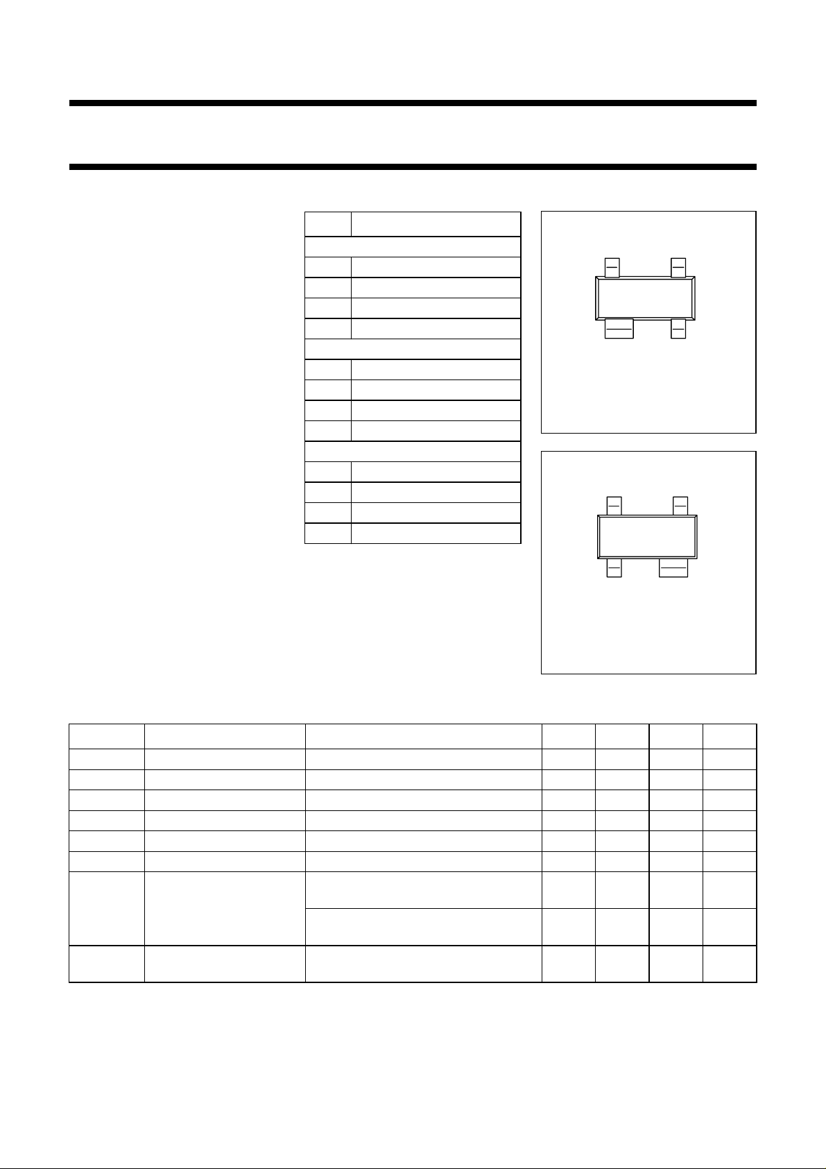
PINNING
PIN DESCRIPTION
BFG197 (Fig.1) Code: V5
1 collector
2 base
3 emitter
4 emitter
BFG197/X (Fig.1) Code: V13
1 collector
2 emitter
3 base
4 emitter
BFG197A/XR (Fig.2) Code: V35
1 collector
2 emitter
3 base
4 emitter
BFG197; BFG197/X;
BFG197/XR
handbook, 2 columns
12
Top view
Fig.1 SOT143.
handbook, 2 columns
34
MSB014
43
12
Top view
MSB035
Fig.2 SOT143XR.
QUICK REFERENCE DATA
SYMBOL PARAMETER CONDITIONS MIN. TYP. MAX. UNIT
V
CBO
V
CEO
I
C
P
tot
C
re
f
T
G
UM
F noise figure Γ
collector-base voltage open emitter −−20 V
collector-emitter voltage open base −−10 V
collector current DC value −−100 mA
total power dissipation up to Ts=75°C; note 1 −−350 mW
feedback capacitance IC=ic= 0; VCB= 8 V; f = 1 MHz − 0.85 − pF
transition frequency IC= 50 mA; VCE= 4 V; f = 2 GHz − 7.5 − GHz
maximum unilateral
power gain
IC= 50 mA; VCE=6V;
T
=25°C; f = 1 GHz
amb
I
= 50 mA; VCE=6V;
C
T
=25°C; f = 2 GHz
amb
= Γ
; IC= 15 mA; VCE=8V;
s
opt
T
=25°C; f = 1 GHz
amb
− 16 − dB
− 10 − dB
− 1.7 − dB
Note
1. T
is the temperature at the soldering point of the collector tab.
S
1995 Sep 13 2
Page 3
Philips Semiconductors Product specification
NPN 7 GHz wideband transistor
BFG197; BFG197/X;
BFG197/XR
LIMITING VALUES
In accordance with the Absolute Maximum System (IEC 134).
SYMBOL PARAMETER CONDITIONS MIN. MAX. UNIT
V
CBO
V
CEO
V
EBO
I
C
P
tot
T
stg
T
j
THERMAL CHARACTERISTICS
SYMBOL PARAMETER VALUE UNIT
R
th j-s
Note
1. T
S
collector-base voltage open emitter − 20 V
collector-emitter voltage open base − 10 V
emitter-base voltage open collector − 2.5 V
collector current DC value, continuous − 100 mA
total power dissipation up to Ts=75°C; note 1 − 350 mW
storage temperature range −65 +150 °C
junction operating temperature − 175 °C
from junction to soldering point; note 1 290 K/W
is the temperature at the soldering point of the collector tab.
CHARACTERISTICS
=25°C unless otherwise specified.
T
j
SYMBOL PARAMETER CONDITIONS MIN. TYP. MAX. UNIT
I
CBO
h
FE
C
c
C
e
C
re
f
T
G
UM
F noise figure Γ
d
2
collector leakage current IE= 0; VCB=5V −−100 nA
DC current gain IC= 50 mA; VCE=5V 40 110 −
collector capacitance IE=ie= 0; VCB= 8 V; f = 1 MHz − 1.5 − pF
emitter capacitance IC=ic= 0; VEB= 0.5 V; f = 1 MHz − 3.3 − pF
feedback capacitance IC=ic= 0; VCB=8V; f=1MHz − 0.85 − pF
transition frequency IC= 50 mA; VCE= 4 V; f = 2 GHz − 7.5 − GHz
maximum unilateral power gain
(note 1)
second order intermodulation
IC= 50 mA; VCE=6V;
T
=25°C; f = 1 GHz
amb
= 50 mA; VCE=6V;
I
C
T
=25°C; f = 2 GHz
amb
= Γ
; IC= 15 mA; VCE=8V;
s
opt
T
=25°C; f = 1 GHz
amb
= Γ
Γ
T
; IC= 50 mA; VCE=6V;
s
opt
=25°C; f = 2 GHz
amb
− 16 − dB
− 10 − dB
− 1.7 − dB
− 2.3 − dB
VCE=6V;Vo= 50 dBmV; −−51 − dB
distortion
Note
1. G
is the maximum unilateral power gain, assuming S12 is zero and
UM
G
UM
10
-----------------------------------------------------------1s
–()1s
2
s
21
2
11
2
–()
22
dB.log=
1995 Sep 13 3
Page 4
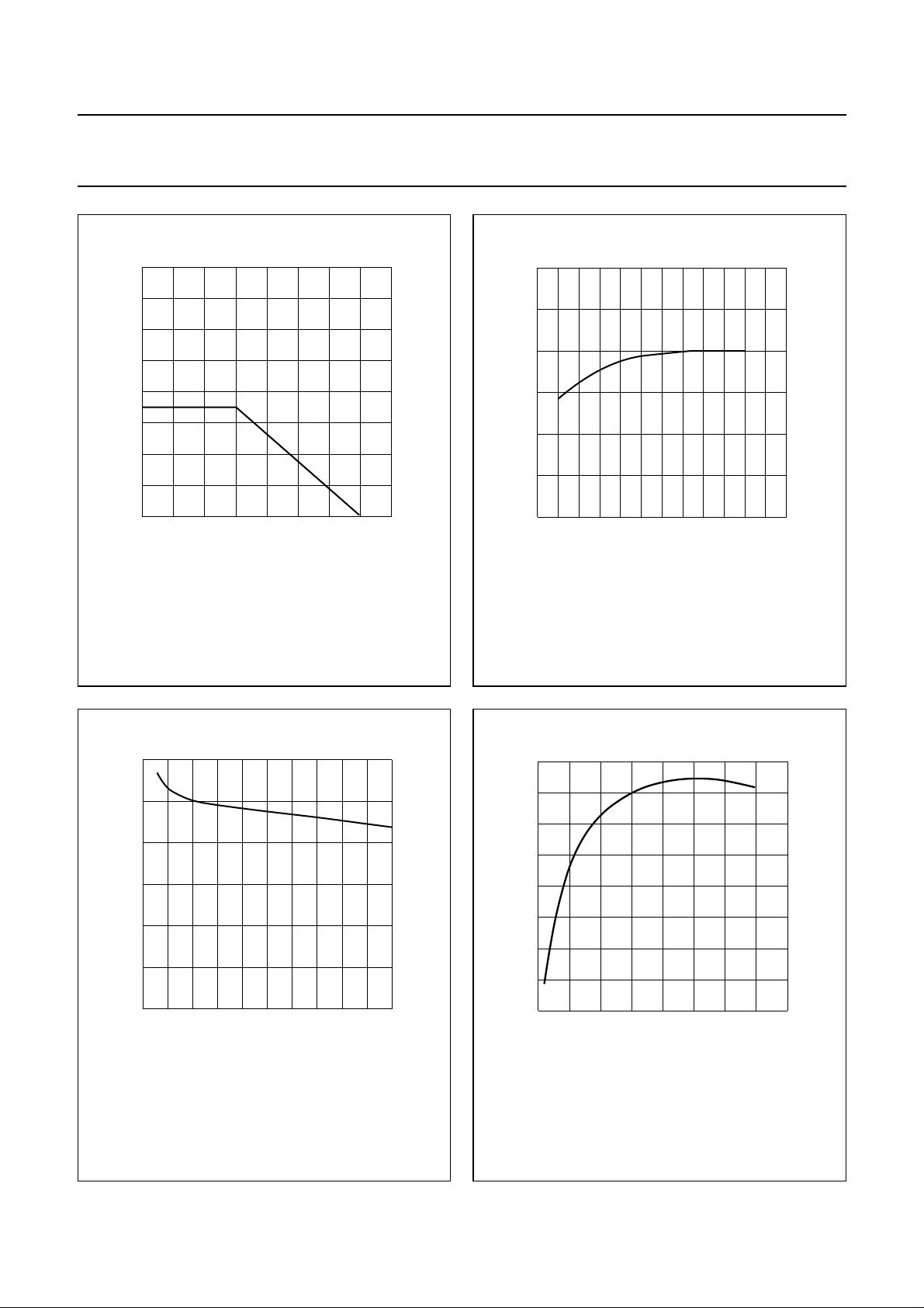
Philips Semiconductors Product specification
NPN 7 GHz wideband transistor
150
MBC983 - 2
o
Ts(
C)
800
handbook, halfpage
P
tot
(mW)
600
400
200
0
0 50 100 200
160
handbook, halfpage
h
FE
120
80
40
0
BFG197; BFG197/X;
BFG197/XR
MBB267
40 120
80
I (mA)
C
1.2
handbook, halfpage
C
re
(pF)
0.8
0.4
0
0
VCE=5V.
Fig.4 DC current gain as a function of collector
Fig.3 Power derating curve.
MCD155
210
468
V (V)
CB
handbook, halfpage
8
f
T
(GHz)
6
4
2
0
02040 80
current.
60
MCD156
I (mA)
C
IC=ic= 0; f= 1MHz.
Fig.5 Feedback capacitance as a function of
collector-base voltage.
1995 Sep 13 4
VCE= 4 V; T
=25°C; f = 2 GHz.
amb
Fig.6 Transition frequency as a function of
collector current.
Page 5

Philips Semiconductors Product specification
NPN 7 GHz wideband transistor
60
MCD157
I (mA)
C
20
handbook, halfpage
gain
(dB)
15
10
5
0
02040 80
MSG
G
max
G
UM
50
handbook, halfpage
gain
(dB)
40
30
20
10
0
10
MSG
BFG197; BFG197/X;
BFG197/XR
MCD158
G
UM
G
max
2
10
3
10
f (MHz)
10
4
VCE= 4 V; f = 1 GHz.
Fig.7 Gain as a function of collector current.
50
handbook, halfpage
gain
(dB)
40
30
20
10
0
10
MSG
G
UM
G
max
2
10
3
10
f (MHz)
MCD159
VCE= 4 V; IC=50mA.
Fig.8 Gain as a function of frequency.
max
f (MHz)
MCD160
4
10
50
handbook, halfpage
gain
(dB)
40
30
20
10
4
10
0
10
MSG
G
UM
G
2
10
3
10
VCE= 6 V; IC= 50mA.
Fig.9 Gain as a function of frequency.
1995 Sep 13 5
VCE= 8V; IC=30mA.
Fig.10 Gain as a function of frequency.
Page 6

Philips Semiconductors Product specification
NPN 7 GHz wideband transistor
MCD161
f = 2 GHz
1 GHz
500 MHz
C
F
(dB)
4
3
2
1
0
handbook, halfpage
101
I (mA)
100
(dB)
F
4
3
2
I = 50 mA
C
20 mA
1
10 mA
0
2
10
handbook, halfpage
BFG197; BFG197/X;
BFG197/XR
MCD162
3
10
f (MHz)
4
10
VCE=6V.
Fig.11 Minimum noise figure as a function of
collector current.
45
handbook, halfpage
d
im
(dB)
50
55
60
65
70
20 120
40 60 80 100
MBB266
I (mA)
C
VCE=6V.
Fig.12 Minimum noise figure as a function of
frequency.
35
handbook, halfpage
d
2
(dB)
40
45
50
55
60
20 120
40 60 80 100
MBB268
I (mA)
C
VCE=8V; Vo= 700 mV; f
= 793.25 MHz; T
(p+q−r)
amb
=25°C.
Fig.13 Intermodulation distortion, typical values.
1995 Sep 13 6
VCE= 8 V; Vo= 50 mV; f
(p+q−r)
= 810MHz; T
amb
=25°C.
Fig.14 Second order intermodulation distortion,
typical values.
Page 7

Philips Semiconductors Product specification
NPN 7 GHz wideband transistor
handbook, full pagewidth
0.5
MSG
23 dB
0.2
+
j
unstable region
0
–
j
stability
circle
0.2
0.5
4 dB
3 dB
2 dB
OPT
*
F = 1.7 dB
min
0.50.2 10521
BFG197; BFG197/X;
BFG197/XR
1
2
5
10
∞
10
5
2
Zo=50Ω.
Maximum stable gain = 23 dB.
handbook, full pagewidth
+ j
– j
G
max
15.8 dB
1
MCD163
Fig.15 Noise circle figure.
1
0.5
5 dB
4 dB
0.2
0
3 dB
OPT
*
F = 2.4 dB
min
*
15 dB
0.2
14 dB
2
5
10
∞
105210.2 0.5
10
5
0.5
Zo=50Ω.
Fig.16 Noise circle figure.
1995 Sep 13 7
2
1
MCD164
Page 8

Philips Semiconductors Product specification
NPN 7 GHz wideband transistor
handbook, full pagewidth
0.5
0.2
F = 3.5 dB
min
+ j
0
– j
0.2
G
max
9.7 dB
0.2
0.2
0.5
OPT
*
*
6 dB
5 dB
4 dB
0.5 1 1052
8 dB
9 dB
BFG197; BFG197/X;
BFG197/XR
1
2
5
10
∞
10
5
2
1
MCD165
Zo=50Ω.
handbook, full pagewidth
Fig.17 Noise circle figure.
1
0.5
3 GHz
0.2
+
j
0
–
j
0.2
0.5
0.5 1 10520.2
40 MHz
2
5
10
∞
10
5
2
VCE= 6 V; IC= 50mA.
Fig.18 Common emitter input reflection coefficient (S11).
1995 Sep 13 8
1
MCD166
Page 9

Philips Semiconductors Product specification
NPN 7 GHz wideband transistor
handbook, full pagewidth
o
135
o
180
_o
135
40 MHz
BFG197; BFG197/X;
BFG197/XR
o
90
o
45
20406080100
3 GHz
_
o
45
o
0
VCE= 6 V; IC= 50mA.
handbook, full pagewidth
_90o
MCD167
Fig.19 Common emitter forward transmission coefficient (S21).
o
90
180
o
135
o
_
o
135
0.040.080.120.160.20
40 MHz
3 GHz
o
45
_
o
45
o
0
VCE= 6 V; IC= 50mA.
_90o
Fig.20 Common emitter reverse transmission coefficient (S12).
1995 Sep 13 9
MCD169
Page 10

Philips Semiconductors Product specification
NPN 7 GHz wideband transistor
handbook, full pagewidth
0.5
0.2
+
j
0
–
j
0.2
3 GHz
0.5
BFG197; BFG197/X;
BFG197/XR
1
2
5
10
0.5 10.2 1052
∞
10
5
40 MHz
2
VCE= 6 V; IC= 50mA.
1
MCD168
Fig.21 Common emitter output reflection coefficient (S22).
1995 Sep 13 10
Page 11

Philips Semiconductors Product specification
NPN 7 GHz wideband transistor
SPICE parameters for BFQ195 crystal
SEQUENCE No. PARAMETER VALUE UNIT
1 IS 1.972 fA
2 BF 150.0 −
3 NF 990.8 m
4 VAF 54.72 V
5 IKF 30.00 A
6 ISE 47.82 fA
7 NE 1.580 −
8 BR 165.4 −
9 NR 993.9 m
10 VAR 2.351 V
11 IKR 9.967 A
12 ISC 3.510 aA
13 NC 1.124 −
14 RB 5.000 Ω
15 IRB 1.000 µA
16 RBM 5.000 Ω
17 RE 368.1 mΩ
18 RC 937.2 mΩ
19 (note 1) XTB 0.000 −
20 (note 1) EG 1.110 EV
21 (note 1) XTI 3.000 −
22 CJE 3.388 pF
23 VJE 600.0 mV
24 MJE 302.9 m
25 TF 11.06 ps
26 XTF 30.02 −
27 VTF 1.649 V
28 ITF 401.9 mA
29 PTF 0.000 deg
30 CJC 1.190 pF
31 VJC 160.1 mV
32 MJC 89.44 m
33 XCJC 130.0 m
34 TR 2.148 ns
35 (note 1) CJS 0.000 F
36 (note 1) VJS 750.0 mV
37 (note 1) MJS 0.000 −
38 FC 785.9 m
BFG197; BFG197/X;
BFG197/XR
handbook, halfpage
L1 L2
B
C
QLB= 50; QLE= 50.
QL
(f) = QL
B,E
Fc = scaling frequency = 1000 MHz.
L
be ce
√ (f/Fc).
B,E
Fig.22 Package equivalent circuit SOT143;
SOT143R.
List of components (see Fig.22)
DESIGNATION VALUE UNIT
C
be
C
cb
C
ce
L1 0.12 nH
L2 0.21 nH
L3 0.06 nH
L
B
L
E
C
cb
B
E'
L
E
L3
E
84 fF
17 fF
191 fF
0.95 nH
0.40 nH
CB' C'
C
MBC964
Note
1. These parameters have not been extracted,
the default values are shown.
1995 Sep 13 11
Page 12

Philips Semiconductors Product specification
NPN 7 GHz wideband transistor
PACKAGE OUTLINES
handbook, full pagewidth
10
max
0.75
0.60
o
max
1.1
30
max
0.150
0.090
0.1
max
10
max
o
BFG197; BFG197/X;
BFG197/XR
3.0
2.8
1.9
43
o
1
2
0.88
0
0.1
TOP VIEW
0.48
1.7
0
0.1
B
A
1.4
1.2
M0.1 AB
2.5
max
0.2
MBC845
M
AB
Dimensions in mm.
handbook, full pagewidth
0.40
0.25
10
max
Fig.23 SOT143.
3.0
0.150
0.090
30
max
o
0.1
max
10
max
o
0.48
0.38
o
1.1
max
2.8
1.9
34
2
1
0.88
0.78
1.7
M0.1 B
TOP VIEW
B
A
1.4
1.2
MBC844
2.5
max
0.2
A
M
Dimensions in mm.
Fig.24 SOT143R.
1995 Sep 13 12
Page 13

Philips Semiconductors Product specification
NPN 7 GHz wideband transistor
BFG197; BFG197/X;
BFG197/XR
DEFINITIONS
Data sheet status
Objective specification This data sheet contains target or goal specifications for product development.
Preliminary specification This data sheet contains preliminary data; supplementary data may be published later.
Product specification This data sheet contains final product specifications.
Limiting values
Limiting values given are in accordance with the Absolute Maximum Rating System (IEC 134). Stress above one or
more of the limiting values may cause permanent damage to the device. These are stress ratings only and operation
of the device at these or at any other conditions above those given in the Characteristics sections of the specification
is not implied. Exposure to limiting values for extended periods may affect device reliability.
Application information
Where application information is given, it is advisory and does not form part of the specification.
LIFE SUPPORT APPLICATIONS
These products are not designed for use in life support appliances, devices, or systems where malfunction of these
products can reasonably be expected to result in personal injury. Philips customers using or selling these products for
use in such applications do so at their own risk and agree to fully indemnify Philips for any damages resulting from such
improper use or sale.
1995 Sep 13 13
 Loading...