

Page 1
DISCRETE SEMICONDUCTORS
DATA SH EET
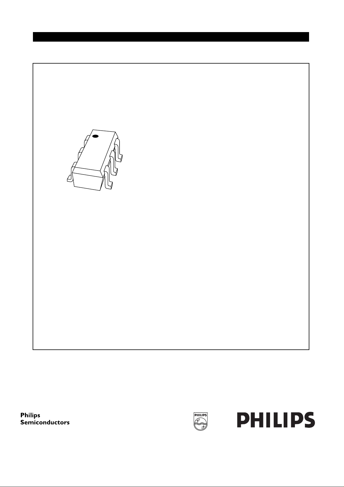
ook, halfpage
MBD128
BF1102; BF1102R
Dual N-channel dual gate
MOS-FETs
Product specification
Supersedes data of 1999 Jul 01
2000 Apr 11
Page 2
Philips Semiconductors Product specification
Dual N-channel dual gate MOS-FETs BF1102; BF1102R
FEATURES
• Two low noise gain controlled amplifiers in a single
package
• Specially designed for 5 V applications
• Superior cross-modulation performance during AGC
• High forward transfer admittance
• High forward transfer admittance to input capacitance
ratio.
APPLICATIONS
Gain controlled low noise amplifier for VHF and UHF
applications such as television tuners and professional
communications equipment.
DESCRIPTION
The BF1102 and BF1102R are both two equal dual gate
MOS-FETs which haveashared source pin and a shared
gate 2 pin. Both devices have interconnected source and
substrate; an internal bias circuit enables DC stabilization
and a very good cross-modulation performance at 5 V
supply voltage; integrated diodes between the gates and
source protect against excessive input voltage surges.
Both devices have a SOT363 micro-miniature plastic
package.
PINNING - SOT363
DESCRIPTION
PIN
BF1102 BF1102R
1 gate 1 (1) gate 1 (1)
2 gate 2 (1 and 2) source (1 and 2)
3 drain (1) drain (1)
4 drain (2) drain (2)
5 source (1 and 2) gate 2 (1 and 2)
6 gate 1 (2) gate 1 (2)
handbook, halfpage
4
56
132
BF1102 marking code: W1.
BF1102R marking code: W2-.
g2 (1, 2)
AMP2
s (1, 2)
Fig.1 Simplified outline and symbol.
AMP1 d (1)g1 (1)
d (2)g1 (2)
MBL029
QUICK REFERENCE DATA
SYMBOL PARAMETER CONDITIONS MIN. TYP. MAX. UNIT
Per MOS-FET unless otherwise specified
V
DS
I
D
P
tot
forward transfer admittance ID=15mA 36 43 − mS
y
fs
C
ig1-s
C
rss
drain-source voltage −−7V
drain current (DC) −−40 mA
total power dissipation Ts≤ 102 °C; note 1 −−200 mW
input capacitance at gate 1 ID=15mA − 2.8 3.6 pF
reverse transfer capacitance f = 1 MHz − 30 50 fF
F noise figure f = 800 MHz − 2 2.8 dB
X
mod
T
j
cross-modulation input level for k = 1% at 40 dB AGC 100 −−dBµV
operating junction temperature −−150 °C
Note
1. T
is the temperature at the soldering point of the source lead.
s
CAUTION
This product is supplied in anti-static packing to prevent damage caused by electrostatic discharge during transport
and handling. For further information, refer to Philips specs.: SNW-EQ-608, SNW-FQ-302A and SNW-FQ-302B.
2000 Apr 11 2
Page 3

Philips Semiconductors Product specification
Dual N-channel dual gate MOS-FETs BF1102; BF1102R
LIMITING VALUES
In accordance with the Absolute Maximum Rating System (IEC 60134).
SYMBOL PARAMETER CONDITIONS MIN. MAX. UNIT
Per MOS-FET unless otherwise specified
V
DS
I
D
I
G1
I
G2
P
tot
T
stg
T
j
THERMAL CHARACTERISTICS
SYMBOL PARAMETER VALUE UNIT
R
th j-s
drain-source voltage − 7V
drain current (DC) − 40 mA
gate 1 current −±10 mA
gate 2 current −±10 mA
total power dissipation Ts≤ 102 °C − 200 mW
storage temperature −65 +150 °C
operating junction temperature − 150 °C
thermal resistance from junction to soldering point 240 K/W
250
handbook, halfpage
P
tot
(mW)
200
150
100
50
0
0 50 100 200
150
Ts (°C)
Fig.2 Power derating curve.
MGS359
2000 Apr 11 3
Page 4
Philips Semiconductors Product specification
Dual N-channel dual gate MOS-FETs BF1102; BF1102R
STATIC CHARACTERISTICS
Tj=25°C unless otherwise specified.
SYMBOL PARAMETER CONDITIONS MIN. MAX. UNIT
Per MOS-FET unless otherwise specified
V
(BR)DSS
V
(BR)G1-SS
V
(BR)G2-SS
V
(F)S-G1
V
(F)S-G2
V
G1-S(th)
V
G2-S(th)
I
DSX
I
G1-S
I
G2-S
drain-source breakdown voltage V
gate 1-source breakdown voltage VGS=VDS= 0; I
gate 2-source breakdown voltage VGS=VDS= 0; I
forward source-gate 1 voltage V
forward source-gate 2 voltage V
gate 1-source threshold voltage VDS=5V; V
gate 2-source threshold voltage VDS=5V; V
drain-source current V
gate 1 cut-off current V
gate 2 cut-off current V
G1-S=VG2-S
G2-S=VDS
G1-S=VDS
=4V; VDS=5V; RG= 120 kΩ; note 1 12 20 mA
G2-S
=5V; V
G1-S
=5V; V
G2-S
= 0; ID=10µA7−V
=10mA 6 15 V
G1-S
=5mA 6 15 V
G2-S
= 0; I
= 0; I
G2-S
G1-S
G2-S=VDS
G1-S=VDS
= 10 mA 0.5 1.5 V
S-G1
= 10 mA 0.5 1.5 V
S-G2
=4V; ID= 100 µA 0.3 1 V
=4V; ID= 100 µA 0.3 1.2 V
=0 − 50 nA
=0 − 20 nA
Note
1. R
connects gate 1 to VGG=5V.
G1
DYNAMIC CHARACTERISTICS
Common source; T
=25°C; V
amb
=4V; VDS=5V; ID= 15 mA; unless otherwise specified.
G2-S
SYMBOL PARAMETER CONDITIONS MIN. TYP. MAX. UNIT
Per MOS-FET unless otherwise specified (note 1)
forward transfer admittance Tj=25°C 364350mS
y
fs
C
ig1-ss
C
ig2-ss
C
oss
C
rss
F noise figure f = 800 MHz; Y
X
mod
input capacitance at gate 1 f = 1 MHz 2 2.8 3.6 pF
input capacitance at gate 2 f = 1 MHz; (note 2) −−7pF
output capacitance f = 1 MHz − 1.6 2.5 pF
reverse transfer capacitance f = 1 MHz − 30 50 fF
− 2 2.8 dB
cross-modulation fw= 50 MHz; f
S=YS opt
= 60 MHz; (note 3)
unw
input level for k = 1% at 0 dB AGC 85 −−dBµV
input level for k = 1% at 40 dB AGC 100 −−dBµV
Notes
1. Not used MOS-FET: V
= 0; VDS=0.
G1-S
2. Gate 2 capacitance of both MOS-FETs.
3. Measured in test circuit of Fig.20.
2000 Apr 11 4
Page 5
Philips Semiconductors Product specification
Dual N-channel dual gate MOS-FETs BF1102; BF1102R
ALL GRAPHS FOR ONE MOS-FET
30
handbook, halfpage
I
D
(mA)
20
10
0
0
VDS=5V.
Tj=25°C.
V
G2-S
0.80.4 2.42.01.61.2
= 4 V
3.5 V
3 V
V
Fig.3 Transfer characteristics; typical values.
160
handbook, halfpage
I
G1
(µA)
120
V
G2-S
= 4 V
2.5 V
G1-S
2 V
1.5 V
1 V
3.5 V
3 V
MGS360
(V)
MGS362
30
handbook, halfpage
I
D
(mA)
20
10
0
010
V
=4V.
G2-S
Tj=25°C.
2468
V
G1-S
= 1.5 V
1.4 V
1.3 V
1.2 V
1.1 V
1 V
Fig.4 Output characteristics; typical values.
50
handbook, halfpage
|yfs|
(mS)
40
V
G2-S
= 4 V
3.5 V
MGS361
VDS (V)
MGS363
3 V
80
40
0
0
VDS=5V.
Tj=25°C.
0.5 2.5
1 1.5 2
2.5 V
2 V
V
G1-S
(V)
Fig.5 Gate 1 current as a function of gate 1
voltage; typical values.
2000 Apr 11 5
30
20
10
0
010 30
VDS=5V.
Tj=25°C.
20
2.5 V
2 V
ID (mA)
Fig.6 Forward transfer admittance as a function
of drain current; typical values.
Page 6

Philips Semiconductors Product specification
Dual N-channel dual gate MOS-FETs BF1102; BF1102R
25
handbook, halfpage
I
D
(mA)
20
15
10
5
0
020 60
VDS= 5 V; V
= 4 V; Tj=25°C.
G2-S
40
MGS364
IG1 (µA)
Fig.7 Draincurrentasafunctionofgate 1 current;
typical values.
15
handbook, halfpage
I
D
(mA)
10
5
0
0
VDS= 5 V; V
RG1= 120 kΩ (connected to VGG); see Fig.20.
1
= 4 V; Tj=25°C.
G2-S
23 54
MGS365
VGG (V)
Fig.8 Draincurrent as a function of gate 1 supply
voltage (= VGG); typical values.
30
handbook, halfpage
I
D
(mA)
20
10
0
010
V
= 4 V; Tj=25°C.
G2-S
RG1 connected to VGG; see Fig.20.
RG1 = 47 kΩ
2468
68 kΩ
VGG = VDS (V)
MGS366
82 kΩ
100 kΩ
120 kΩ
150 kΩ
180 kΩ
220 kΩ
Fig.9 Draincurrentasafunctionofgate 1 (= VGG)
and drain supply voltage; typical values.
20
handbook, halfpage
I
D
(mA)
16
12
8
4
0
02 6
VDS= 5 V; Tj=25°C.
RG1= 120 kΩ (connected to VGG); see Fig.20.
V
G1-S
4
V
G2-S
Fig.10 Drain current as a function of gate 2
voltage; typical values.
MGS367
= 5 V
4.5 V
4 V
3.5 V
3 V
(V)
2000 Apr 11 6
Page 7

Philips Semiconductors Product specification
Dual N-channel dual gate MOS-FETs BF1102; BF1102R
40
handbook, halfpage
I
G1
(µA)
30
20
10
0
0
VDS= 5 V; Tj=25°C.
RG1= 120 kΩ (connected to VGG); see Fig.20.
264
V
G1-S
V
G2-S
Fig.11 Gate 1 current as a function of gate 2
voltage; typical values.
MGS368
= 5 V
4.5 V
4 V
3.5 V
3 V
(V)
handbook, halfpage
0
gain
reduction
(dB)
−10
−20
−30
−40
−50
012 4
VDS= 5 V; VGG= 5 V; f = 50 MHz; T
RG1= 120 kΩ (connected to VGG); see Fig.20.
amb
=25°C;
MCD968
3
V
(V)
AGC
Fig.12 Typical gain reduction as a function of the
AGC voltage; see Fig.20.
120
handbook, halfpage
V
unw
(dBµV)
110
100
90
80
020 60
VDS= 5 V; VGG= 5 V; fw= 50 MHz; f
RG1= 120 kΩ (connected to VGG); see Fig.20.
40
gain reduction (dB)
= 60 MHz; T
unw
MGS369
amb
=25°C;
Fig.13 Unwanted voltage for 1% cross-modulation
as a function of gain reduction;
typical values.
20
handbook, halfpage
I
D
(mA)
16
12
8
4
0
VDS= 5 V; VGG= 5 V; f = 50 MHz; T
RG1= 120 kΩ (connected to VGG); see Fig.20.
10 20 30 40
050
gain reduction (dB)
=25°C;
amb
Fig.14 Drain current as a function of gain
reduction; typical values.
MCD969
2000 Apr 11 7
Page 8

Philips Semiconductors Product specification
Dual N-channel dual gate MOS-FETs BF1102; BF1102R
2
10
handbook, halfpage
y
is
MGS370
(mS)
10
b
is
1
g
is
−1
10
10 10
2
f (MHz)
VDS= 5 V; VG2=4V.
ID= 15 mA; T
amb
=25°C.
Fig.15 Input admittance asafunctionof frequency;
typical values.
f (MHz)
MCD970
3
−10
ϕ
rs
(deg)
2
−10
−10
−1
3
10
3
10
handbook, halfpage
y
rs
(mS)
ϕ
2
10
rs
y
rs
10
3
10
1
10
2
10
VDS= 5 V; VG2=4V.
ID= 15 mA; T
amb
=25°C.
Fig.16 Reverse transfer admittance and phase as
a function of frequency; typical values.
2
10
handbook, halfpage
|yfs|
|yfs|
MGS372
(mS)
ϕ
fs
10
1
10 10
2
f (MHz)
VDS= 5 V; VG2=4V.
ID= 15 mA; T
amb
=25°C.
Fig.17 Forward transfer admittance and phase as
a function of frequency; typical values.
f (MHz)
MCD971
3
10
2
10
−ϕ
fs
(deg)
10
1
3
10
10
handbook, halfpage
y
os
(mS)
1
−1
10
10 10
b
os
g
os
2
VDS= 5 V; VG2=4V.
ID= 15 mA; T
amb
=25°C.
Fig.18 Output admittance as a function of
frequency; typical values.
2000 Apr 11 8
Page 9

Philips Semiconductors Product specification
Dual N-channel dual gate MOS-FETs BF1102; BF1102R
handbook, halfpage
0
crosstalk
level
(dB)
−20
−40
−60
−80
0
200 1000
Active amplifier: VDS= 5 V; VG2= 4 V; ID=15mA.
Non-active amplifier: VDS=V
Source and load impedances: 50 Ω (both amplifiers).
T
=25°C.
amb
400 600 800
=0V.
G1-S
Fig.19 Crosstalk as a function of frequency:
Output level of non-active amplifier related
to output level of active amplifier; typical
values.
MCD972
f (MHz)
V
GG
R1
10 kΩ
R
V
G1
AGC
4.7 nF
handbook, full pagewidth
R
GEN
50 Ω
V
C2
4.7 nF
R2
50 Ω
I
Fig.20 Cross-modulation test set-up (for one MOS-FET).
2000 Apr 11 9
C1
DUT
V
L1
≈2.2 µH
DS
C3
4.7 nF
C4
4.7 nF
MGS315
R
L
50 Ω
Page 10

Philips Semiconductors Product specification
Dual N-channel dual gate MOS-FETs BF1102; BF1102R
Table 1 Scattering parameters: VDS=5V; V
s
f
(MHz)
MAGNITUDE
(ratio)
11
ANGLE
(deg)
MAGNITUDE
(ratio)
=4V; ID= 15 mA; T
G2-S
s
21
ANGLE
(deg)
=25°C
amb
s
12
MAGNITUDE
(ratio)
ANGLE
(deg)
s
22
MAGNITUDE
(ratio)
ANGLE
(deg)
50 0.987 −5.6 4.069 173.5 0.001 95.4 0.986 −3.0
100 0.981 −11.1 4.042 167.0 0.002 81.3 0.983 −6.0
200 0.961 −21.9 3.926 154.4 0.005 75.8 0.976 −12.0
300 0.933 −32.1 3.778 142.4 0.006 69.6 0.960 −17.7
400 0.899 −42.0 3.593 130.6 0.007 65.6 0.945 −23.2
500 0.867 −51.1 3.412 119.6 0.007 64.4 0.928 −29.1
600 0.834 −59.9 3.216 109.2 0.007 67.5 0.914 −34.1
700 0.805 −67.9 3.010 99.0 0.006 78.7 0.901 −39.8
800 0.779 −75.7 2.804 89.2 0.007 92.7 0.886 −45.1
900 0.758 −82.1 2.656 80.3 0.007 120.7 0.889 −49.7
1000 0.740 −89.0 2.509 69.9 0.009 125.5 0.890 −55.7
Table 2 Noise data: V
f
(MHz)
=5V; V
DS
=4V; ID= 15 mA; T
G2-S
F
min
(dB)
=25°C
amb
Γ
opt
(ratio) (deg)
R
(Ω)
n
800 2 0.621 61.61 25.85
2000 Apr 11 10
Page 11

Philips Semiconductors Product specification
Dual N-channel dual gate MOS-FETs BF1102; BF1102R
PACKAGE OUTLINE
Plastic surface mounted package; 6 leads SOT363
D
y
56
pin 1
index
4
132
e
1
e
b
p
wBM
E
H
E
A
A
1
detail X
AB
Q
L
p
X
v M
A
c
0 1 2 mm
scale
DIMENSIONS (mm are the original dimensions)
A
max
0.1
1
b
cD
p
0.30
0.25
0.20
0.10
IEC JEDEC EIAJ
2.2
1.8
E
1.35
1.15
REFERENCES
1.3
e
e
1
0.65
UNIT
mm
A
1.1
0.8
OUTLINE
VERSION
SOT363 SC-88
2000 Apr 11 11
H
E
2.2
2.0
L
p
0.45
0.15
Qywv
0.25
0.15
0.2 0.10.2
EUROPEAN
PROJECTION
ISSUE DATE
97-02-28
Page 12

Philips Semiconductors Product specification
Dual N-channel dual gate MOS-FETs BF1102; BF1102R
DATA SHEET STATUS
DATA SHEET STATUS
Objective specification Development This data sheet contains the design target or goal specifications for
Preliminary specification Qualification This data sheet contains preliminary data, and supplementary data will be
Product specification Production This data sheet contains final specifications. Philips Semiconductors
Note
1. Please consult the most recently issued data sheet before initiating or completing a design.
DEFINITIONS
Short-form specification The data in a short-form
specification is extracted from a full data sheet with the
same type number and title. For detailed information see
the relevant data sheet or data handbook.
Limiting values definition Limiting values given are in
accordance with the Absolute Maximum Rating System
(IEC 60134). Stress above one or more of the limiting
values may cause permanent damage to the device.
These are stress ratings only and operation of the device
attheseor at any other conditions above thosegiveninthe
Characteristics sections of the specification is not implied.
Exposure to limiting values for extended periods may
affect device reliability.
Application information Applications that are
described herein for any of these products are for
illustrative purposes only. Philips Semiconductors make
norepresentationorwarrantythatsuchapplicationswillbe
suitable for the specified use without further testing or
modification.
PRODUCT
STATUS
DEFINITIONS
product development. Specification may change in any manner without
notice.
published at a later date. Philips Semiconductors reserves the right to
make changes at any time without notice in order to improve design and
supply the best possible product.
reserves the right to make changes at any time without notice in order to
improve design and supply the best possible product.
DISCLAIMERS
Life support applications These products are not
designed for use in life support appliances, devices, or
systems where malfunction of these products can
reasonably be expected toresult in personalinjury. Philips
Semiconductorscustomersusingorsellingtheseproducts
for use in such applications do so at their own risk and
agree to fully indemnify Philips Semiconductors for any
damages resulting from such application.
Right to make changes Philips Semiconductors
reserves the right to make changes, without notice, in the
products, including circuits, standard cells, and/or
software, described or contained herein in order to
improve design and/or performance. Philips
Semiconductors assumes no responsibility or liability for
theuseofanyof these products, conveys no licence or title
under any patent, copyright, or mask work right to these
products,and makes no representations or warrantiesthat
these products are free from patent, copyright, or mask
work right infringement, unless otherwise specified.
(1)
2000 Apr 11 12
Page 13

Philips Semiconductors Product specification
Dual N-channel dual gate MOS-FETs BF1102; BF1102R
NOTES
2000 Apr 11 13
Page 14

Philips Semiconductors Product specification
Dual N-channel dual gate MOS-FETs BF1102; BF1102R
NOTES
2000 Apr 11 14
Page 15

Philips Semiconductors Product specification
Dual N-channel dual gate MOS-FETs BF1102; BF1102R
NOTES
2000 Apr 11 15
Page 16

Philips Semiconductors – a w orldwide compan y
Argentina: see South America
Australia: 3 Figtree Drive, HOMEBUSH, NSW 2140,
Tel. +61 2 9704 8141, Fax. +61 2 9704 8139
Austria: Computerstr. 6, A-1101 WIEN, P.O. Box 213,
Tel. +43 1 60 101 1248, Fax. +43 1 60 101 1210
Belarus: Hotel Minsk Business Center, Bld. 3, r. 1211, Volodarski Str. 6,
220050 MINSK, Tel. +375 172 20 0733, Fax. +375 172 20 0773
Belgium: see The Netherlands
Brazil: see South America
Bulgaria: Philips Bulgaria Ltd., Energoproject, 15th floor,
51 James Bourchier Blvd., 1407 SOFIA,
Tel. +359 2 68 9211, Fax. +359 2 68 9102
Canada: PHILIPS SEMICONDUCTORS/COMPONENTS,
Tel. +1 800 234 7381, Fax. +1 800 943 0087
China/Hong Kong: 501 Hong Kong Industrial Technology Centre,
72 Tat Chee Avenue, Kowloon Tong, HONG KONG,
Tel. +852 2319 7888, Fax. +852 2319 7700
Colombia: see South America
Czech Republic: see Austria
Denmark: Sydhavnsgade 23, 1780 COPENHAGEN V,
Tel. +45 33 29 3333, Fax. +45 33 29 3905
Finland: Sinikalliontie 3, FIN-02630 ESPOO,
Tel. +358 9 615 800, Fax. +358 9 6158 0920
France: 51 Rue Carnot, BP317, 92156 SURESNES Cedex,
Tel. +33 1 4099 6161, Fax. +33 1 4099 6427
Germany: Hammerbrookstraße 69, D-20097 HAMBURG,
Tel. +49 40 2353 60, Fax. +49 40 2353 6300
Hungary: see Austria
India: Philips INDIA Ltd, Band Box Building, 2nd floor,
254-D, Dr. Annie Besant Road, Worli, MUMBAI 400 025,
Tel. +91 22 493 8541, Fax. +91 22 493 0966
Indonesia: PTPhilips Development Corporation,Semiconductors Division,
Gedung Philips, Jl. Buncit Raya Kav.99-100, JAKARTA 12510,
Tel. +62 21 794 0040 ext. 2501, Fax. +62 21 794 0080
Ireland: Newstead, Clonskeagh, DUBLIN 14,
Tel. +353 1 7640 000, Fax. +353 1 7640 200
Israel: RAPAC Electronics, 7 Kehilat Saloniki St, PO Box 18053,
TEL AVIV 61180, Tel. +972 3 645 0444, Fax. +972 3 649 1007
Italy: PHILIPS SEMICONDUCTORS, Via Casati,23 - 20052 MONZA (MI),
Tel. +39 039 203 6838, Fax +39 039 203 6800
Japan: Philips Bldg 13-37, Kohnan 2-chome, Minato-ku,
TOKYO 108-8507, Tel. +81 3 3740 5130, Fax. +81 3 3740 5057
Korea: Philips House, 260-199 Itaewon-dong, Yongsan-ku, SEOUL,
Tel. +82 2 709 1412, Fax. +82 2 709 1415
Malaysia: No. 76 Jalan Universiti, 46200 PETALING JAYA, SELANGOR,
Tel. +60 3 750 5214, Fax. +60 3 757 4880
Mexico: 5900 Gateway East, Suite 200, EL PASO, TEXAS 79905,
Tel. +9-5 800 234 7381, Fax +9-5 800 943 0087
Middle East: see Italy
Netherlands: Postbus 90050, 5600 PB EINDHOVEN, Bldg. VB,
Tel. +31 40 27 82785, Fax. +31 40 27 88399
New Zealand: 2 Wagener Place, C.P.O. Box 1041, AUCKLAND,
Tel. +64 9 849 4160, Fax. +64 9 849 7811
Norway: Box 1, Manglerud 0612, OSLO,
Tel. +47 22 74 8000, Fax. +47 22 74 8341
Pakistan: see Singapore
Philippines: Philips Semiconductors Philippines Inc.,
106 Valero St. Salcedo Village, P.O. Box 2108 MCC, MAKATI,
Metro MANILA, Tel. +63 2 816 6380, Fax. +63 2 817 3474
Poland: Al.Jerozolimskie 195 B, 02-222 WARSAW,
Tel. +48 22 5710 000, Fax. +48 22 5710 001
Portugal: see Spain
Romania: see Italy
Russia: Philips Russia, Ul. Usatcheva 35A, 119048 MOSCOW,
Tel. +7 095 755 6918, Fax. +7 095 755 6919
Singapore: Lorong 1, Toa Payoh, SINGAPORE 319762,
Tel. +65 350 2538, Fax. +65 251 6500
Slovakia: see Austria
Slovenia: see Italy
South Africa: S.A. PHILIPS Pty Ltd., 195-215 Main Road Martindale,
2092 JOHANNESBURG, P.O. Box 58088 Newville 2114,
Tel. +27 11 471 5401, Fax. +27 11 471 5398
South America: Al. Vicente Pinzon, 173, 6th floor,
04547-130 SÃO PAULO, SP, Brazil,
Tel. +55 11 821 2333, Fax. +55 11 821 2382
Spain: Balmes 22, 08007 BARCELONA,
Tel. +34 93 301 6312, Fax. +34 93 301 4107
Sweden: Kottbygatan 7, Akalla, S-16485 STOCKHOLM,
Tel. +46 8 5985 2000, Fax. +46 8 5985 2745
Switzerland: Allmendstrasse 140, CH-8027 ZÜRICH,
Tel. +41 1 488 2741 Fax. +41 1 488 3263
Taiwan: Philips Semiconductors, 6F, No. 96, Chien Kuo N. Rd., Sec. 1,
TAIPEI, Taiwan Tel. +886 2 2134 2886, Fax. +886 2 2134 2874
Thailand: PHILIPS ELECTRONICS (THAILAND) Ltd.,
209/2 Sanpavuth-Bangna Road Prakanong, BANGKOK 10260,
Tel. +66 2 745 4090, Fax. +66 2 398 0793
Turkey: Yukari Dudullu, Org. San. Blg., 2.Cad. Nr. 28 81260 Umraniye,
ISTANBUL, Tel. +90 216 522 1500, Fax. +90 216 522 1813
Ukraine: PHILIPS UKRAINE, 4 Patrice Lumumba str., Building B, Floor 7,
252042 KIEV, Tel. +380 44 264 2776, Fax. +380 44 268 0461
United Kingdom: Philips Semiconductors Ltd., 276 Bath Road, Hayes,
MIDDLESEX UB3 5BX, Tel. +44 208 730 5000, Fax. +44 208 754 8421
United States: 811 East Arques Avenue, SUNNYVALE, CA 94088-3409,
Tel. +1 800 234 7381, Fax. +1 800 943 0087
Uruguay: see South America
Vietnam: see Singapore
Yugoslavia: PHILIPS, Trg N. Pasica 5/v, 11000 BEOGRAD,
Tel. +381 11 3341 299, Fax.+381 11 3342 553
For all other countries apply to: Philips Semiconductors,
International Marketing & Sales Communications, Building BE-p, P.O. Box 218,
5600 MD EINDHOVEN, The Netherlands, Fax. +31 40 27 24825
© Philips Electronics N.V. SCA
All rights are reserved. Reproduction in whole or in part is prohibited without the prior written consent of the copyright owner.
The information presented in this document does not form part of any quotation or contract, is believed to be accurate and reliable and may be changed
without notice. No liability will be accepted by the publisher for any consequence of its use. Publication thereof does not convey nor imply any license
under patent- or other industrial or intellectual property rights.
2000
Internet: http://www.semiconductors.philips.com
69
Printed in The Netherlands 603504/03/pp16 Date of release: 2000 Apr 11 Document order number: 9397 750 06919
 Loading...