

Page 1
BA1451F
Audio ICs
AM radio / FM IF stereo system IC
BA1451F
The BA1451F is a tuner system IC for electronic tuning for AM radios, FM IF, and MPX. It has been developed for HiFi
component applications.
The MPX VCO circuit requires no adjustment, which will enable a reduction in the number of production line processes.
In particular, the laser lock technique used in the VCO means that no external adjustment is required.
Applications
!
Synthesized tuner for HiFi components.
Features
!
1) Built-in AM monaural radio, FM IF amplifier/detector, and FM stereo demodulator.
2) DTS (both SD and IF count) compatible.
3) Built-in reference voltage power supply provides good shortwave band frequency stability.
4) Good FM stability.
5) The FM MPX VCO uses laser locking making adjustment and external components unnecessary.
6) Built-in forced monaural operation function for MPX (VCO stops, and LED goes off).
7) Low cutoff of audio is possible to improve AM fidelity.
8) MPX VCO stops in AM mode.
9) Audio muting is possible when an IF request is made.
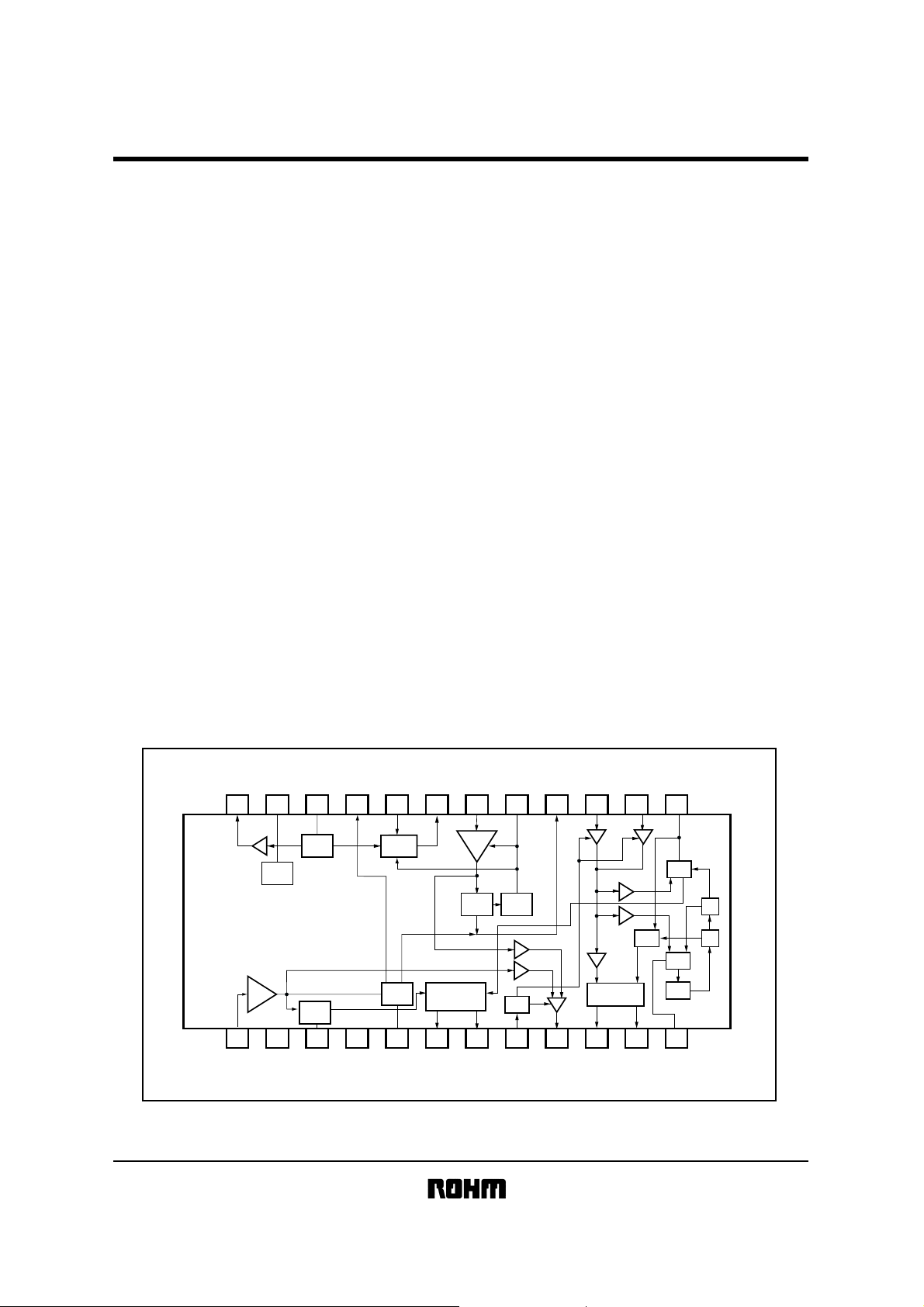
Block diagram
!!!!
24 23 22 21 20 19 18 17 16 15 14 13
LED
DRIVER
AM IF
AM
DET
AGC
COMP
DECODER
SD
SW
PD
VCO
AM
OSC
Vreg
FM
IF
123456789101112
SD
DET
GNDVcc
AM
MIX
FM
DET
1/2
1/2
Page 2
Audio ICs
Absolute maximum ratings
!!!!
Parameter Symbol Limits Unit
Power supply voltage
Power dissipation
Operating temperature
Storage temperature
1 Reduced by 4.5mW for each increase in Ta of 1˚C over 25˚C.
∗
Recommended operating conditions
!!!!
Parameter Symbol Min. Typ. Max. Unit
Power supply voltage
Input and output circuits
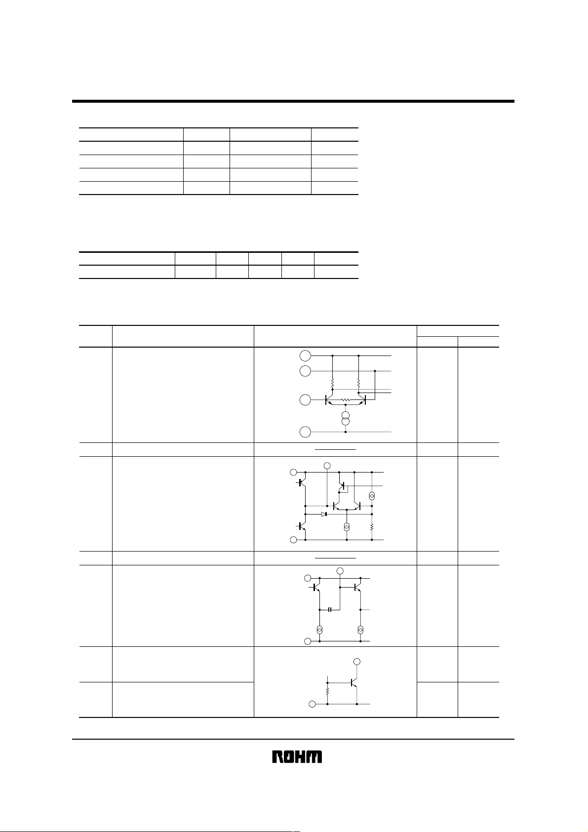
!!!!
Pin No.
Function
V
CC
Pd 450
Topr −25∼+75 ˚C
Tstg −55∼+125 ˚C
(Ta=25°C)
CC
3.8 5.0 8.0 VV
9.0 V
1
∗
mW
Internal circuit
2
V
CC
V
23
reg
BA1451F
Quiescent voltage (V)
FM AM
FM IF amplifier input
1 2.1 2.1
Connect to an FM ceramic filter.
V
CC
2 5.0 5.0
1
4
GND
2
V
CC
330Ω
3
FM tuning ON level adjustment
3 0.25 0
Connect a resistor from this pin to GND
to set the required ON level for
the tuning indicator.
4
GND
GND
4 00
24V
CC
FM discriminator
5 5.0
Connect to the discriminator coil.
GND
5
5pF
Tuning indicator
6 −−
Connect to a tuning indicator
15kΩ
5.0
6/7
display device (eg. LED)
Stereo indicator
Connect to a stereo indicator
7 −−
display device (eg. LED)
4GND
Page 3
Audio ICs
BA1451F
Pin No.
· IF request
Output the IF signal to pin9 excess
of 4.0V.
Stops the IF signal at equal to or less
than 3.0V.
8 00
Function Internal circuit
10k
MUTE
Ω
10kΩ
8
IF OUT
Quiescent pin voltage (V)
FM AM
· MUTE
Apply to muting excess of 2.0V.
Off the muting at equal to or less
than 1.0V.
IF output
9 4.2 4.2
Output for the IF signal.
10 1.5 1.5
R-channel output
11 1.5 1.5
L-channel output
GND
V
GND
V
GND
CC
4
2
CC
9
4
2
10/11
5kΩ
4
23
V
· PLL filter
reg
Connect to a lag/lead filter.
12 0
12
82kΩ
AM/FM
2.1
· AM / FM band switch
AM band when connected to GND.
4
GND
· Forced monaural
Forced monaural operation connecting
to get a resistor to mediate.
(Recommended value : 10kΩ to
13
ground.)
23
V
reg
13
4kΩ
MONO
2.1 2.1
· Pilot filter
GND
Connect to a capacitor.
4
Page 4

Audio ICs
BA1451F
Pin No.
14
15
Function Internal circuit
MPX input
Input the FM detector output .
MPX input
Input the AM detector output after
low cut.
V
V
GND
V
2
CC
23
reg
20kΩ
100kΩ
14
15
4
CC
Quiescent pin voltage (V)
FM AM
2.1 2.1
2.12.1
AM/FM detector output
16
Connect to the following stage MPX and
5kΩ
16
2.1 2.1
FM low pass filter.
GND24
17
2
V
CC
AM AGC
17 00
Connect to a capacitor.
20kΩ
GND
4
2
V
CC
3kΩ
18
AM IF input
18 5.0 5.0
Connect to an AM ceramic filter.
GND
4
2
V
AM mixer output
19 5.0 5.0
CC
23
V
reg
19
Connect to primary side of AM IFT.
20
30kΩ
AM antenna
20 2.1 2.1
Connect to AM antenna.
4
GND
Page 5

Audio ICs
BA1451F
Pin No.
Function Internal circuit
CC
2
V
21
Quiescent pin voltage (V)
FM AM
FM detector bandwidth adjustment
21 2.1 2.1
Connect a resistor from this pin to the
reference voltage supply to set the
required detector bandwidth.
4
GND
Reference voltage supply
23 2.1 2.1
Connected to a capacitor.
AM local oscillator
reg
V
22 2.1 2.1
23
Connect to the AM OSC circuit.
4.3kΩ
22
100Ω
24
AM local oscillator output
24 1.7 1.4
4
AM OSC output.
Electrical characteristics
!!!!
FM IF MPX signal source : fi
19kHz 7.5kHzdev (10%)
AM
(Unless otherwise specified, Ta=25°C and VCC=5V)
N
=10.7MHz, modulation 1kHz, 75kHzdev (100%)
: fiN=1000kHz, modulation 1kHz 30%
GND
Parameter Symbol Min. Typ. Max. Unit Conditions
Quiescent current FM
Quiescent current AM
Q (FM)
I
Q (AM)
I
13 21
11 19 mA
29 mA
27
No input
No input
<FM IF MPX>
Detector output voltage
−3dB limiting sensitivity
Signal-to-noise ratio
Channel balance
AM suppression ratio
Channel separation
Total harmonic distortion
Station detector sensitivity
Station detector bandwidth
IF OUT output voltage
V
L.S 40 dBµV mono
S / N − dB V
340 480 670
O
34 37
72 80
C.B −20+2dBV
AMR − dB
45 55
SEP 35 45 − dB VIN=100dBµV, main
THD − %V
S
SD
SD
V
34 39 44
SW
70 150
IF
300 400 530
0.5 1.6
100 VIN=100dBµV, mono
mVrms VIN=100dBµV,mono
IN
=100dBµV, mono
IN
=100dBµV, mono
AM : VIN=
60dBµV, mod=30% , 400Hz
IN
=100dBµV, main
dBµV
Input for pin 6 current ≥ 1mA
kHz
mV
P-P
IF request ON
<AM>
Detector output voltage
Usable sensitivity
Signal-to-noise ratio
Total harmonic distortion
Station detector sensitivity
IF OUT output voltage
Local buffer output voltage
V
Q.S dBµV
70
O
22 25 28
S / N 42 52 − dB V
THD − 0.6 1.8 % V
S
V
SD
V
OBuff
21 26 31
IF
300 400 530
140 200 280 mVrms
90 120 mVrms VIN=68dBµV
Input for S / N = 20dB
IN
=68dBµV
IN
=68dBµV
dBµV
mV
Input for pin 6 current ≥ 1mA
P-P
IF request ON
Page 6

Audio ICs
Test cir cu i t
!!!!
47p
SG
OSC OUT
AM SG
MIX
AM STEREO
T2
100p
22
DET
L4
100
20k
0.022
24 23 22 21 20 19 18 17 16 15 14 13
0.022
Vreg
OSC
0.022
50
100
6800p 1
BA1451F
MONO
10
10k
STEREO
FM STEREO SG
FM SG
SG SG
Vreg
SD
LEDDET
123456789101112
0.022
50
100
L4
: AM OSC
T2
: AM IFT
CD1
: FM DISCRIMINATOR COIL
1
0. 022
GNDVcc
ST.TUN.
3.9k
24k
+B
Sumida
Toko
Toko
Sumida
Toko
MUTE
REQ.
IFREQ
MUTE
2157-JPS-029
A7BRS-12445X
CFMA-258
0236-JPS-101
A119ACS-19197N
OFF
0.022
Units : R [Ω]
MPX
0.010.01
C [µF]
Fig. 1
0.22
3.3k
L-chR-chIF OUT
AM
FM
0.047
Page 7

Audio ICs
Application example
!!!!
BA1451F
5678
BA4425F
BPF
Electrical characteristic curves
!!!!
4321
Vcc2 (+9V)
0
−10
7
−20
−30
6
−40
5
Vcc=5V,
−50
4
f
IN
=10.7MHz,
fm=1kHz
−60
3
Vo, AMR, SEP (dB)
∆f=±22.5kHzdev,
pilot=±7.5kHzdev
−70
2
Ta=25˚C,
AMR MOD=30%,
1
−80
fm=400Hz
0
−90
TOTAL HARMONIC DISTORTION : THD (%)
−
20 100 120
20 40 80
060
INPUT VOLTAGE : V
Fig.3 FM input / output characteristics
XOUT
BU2616F
DA
CE
µ-COM
S+D+N
N
D+N (100%)
D+N (30%)
IN
(
dBµ)
CL
Fig. 2
AMR
R→L
SEP
L→R
OSC
OUT
131415161718192021222324
MIXOUT
AM INBW Adj
AMVreg
SDMPXMPXDETAGCIFIN
ININOUTAM AMOSC
/
MONO
BA1451F
MUTE
/
IF OUTIF REQ
STTUN
FM DET
GND
SD Adj
VDDFMIN
101112131415161718
P0P1P2AMINFMINVDDPD1PD2GND
P3IFINSDTUNCLDACEXIN
987654321
TUNING
TO LED etc.
STEREO
180
110
170
100
160
90
150
80
140
70
130
60
120
50
Vo (mVrms)
110
40
100
30
90
20
−3dBL, S, TUNED ON (dBµ) SEP (dB)
80
10
70
11
10
9
8
7
6
5
R→L
4
3
2
1
TOTAL HARMONIC DISTORTION : THD (%)
0
0
3456789
PD
/
AMFMLchRch
121110987654321
L→R
V
TUNED ON
−3dB L.S.
D+N (100%)
D+N (30%)
fIN=10.7MHz,
O
V
IN
=100dBµ,
∆f=±22.5kHzdev.
(pilot=±7.5kHzdev)
f
IN
=1kHz,
Ta=25˚C,
RSD=20kΩ
Vcc (5V)
Lch OUT
Rch OUT
POWER SUPPLY VOLTAGE : VCC (V)
Fig.4 FM characteristics vs.
power suppy voltage
Page 8

Audio ICs
BA1451F
TOTAL HARMONIC DISTORTION : THD (%)
10.80
10.75
(MHz)
IN
10.70
10.65
10.60
FM BAND WIDTH : f
10.55
3
RBW=20kΩ, VIN=100dBµ
Ta=25˚C
4567
POWER SUPPLY VOLTAGE : Vcc (V)
Fig.5 FM bandwidth vs.
power supply voltage
10
0
(dB)
−10
O
10
−20
9
8
−30
7
6
−40
5
V
4
3
2
1
0
OUT
−50
f
IN
OUTPUT VOLTAGE : V
f
m
=1kHz
−60
MOD=30%,
Ta=25˚C
−70
−20
=5V,
=1000kHz,
0
INPUT VOLTAGE : V
S+D+N
S / N=20dB
D+N (80%)
D+N (30%)
LED ON
50 100
N
IN
Fig.7 AM input / output characteristics
V
AGC
(dBµ)
8
9
3.0
2.0
(V)
AGC
V
1.0
0
120
60
2
50
40
30
1
20
10
CHANNEL SEPARATION : SEP (dB)
TOTAL HARMONIC DISTORTION : THD (%)
0
0
Vcc=5V
f
IN
=10.7MHz
V
IN
=100dBµ
∆f=±22.5kHzdev
pilot=±7.5kHzdev
Ta=25˚C
200 500 1k 2k5k10k
50
100
FREQUENCY : fm (Hz)
Fig.6 Channel separation and
THD vs. frequency
10
100
Q.S. , TUNED ON : (dBµ)
100
9
90
80
70
60
50
40
30
20
10
90
8
80
7
70
fIN=1000kHz,
V
IN
6
5
4
3
2
1
0
0
TOTAL HARMONIC DISTORTION : THD (%)
=74dBµ,
60
MOD=30%
50
f
m
=1kHz,
Ta=25˚C
40
30
20
OUTPUT VOLTAGE : Vo (mVrms)
10
0
34 56789
POWER SUPPLY VOLTAGE : VCC (V)
Fig.8 AM characteristics vs.
power suppy voltage
THD
Vo
Q.S.
D+N (80%)
D+N (30%)
SEP
TUNED ON
R→L
MAIN
L→R
MONO
R
L
SUB
20k
10
(dBm)
O
0
−10
10
−20
−30
−40
5
−50
V
f
IN
V
MOD
Ta
CC
=
IN
=
5V
1000MHz
=
74dBµ
=
30%
=
25˚C
D+N (80%)
−60
TOTAL HARMONIC DISTORTION : THD (%)
0
−70
AM DETECTOR OUTPUT VOLTAGE : V
50 100 200 500 1k 2k 5k 10k 20k
FREQUENCY : fm (Hz)
Fig.9 AM detector output and
THD vs. frequency
V
O
D+N (30%)
External dimensions
!!!!
24
5.4 ± 0.2
7.8 ± 0.3
1
1.8 ± 0.1
1.27
0.11
(Units : mm)
15.0 ± 0.2
0.4 ± 0.1
SOP24
13
12
0.15 ± 0.1
0.3Min.
0.15
 Loading...