

Page 1
Integrated
Circuit
Systems, Inc.
General Description Features
ICS1889
Block Diagram
PHYceiver and QuickPoll are trademarks of Integrated Circuit Systems, Inc.
100Base-FX Integrated PHYceiver
TM
ICS1889RevF092497P
One chip integrated physical layer
All CMOS, low power design
ISO/IEC 8802-3 CSMA/CD compliant
100Base-FX Half & Full Duplex
Far end fault detection
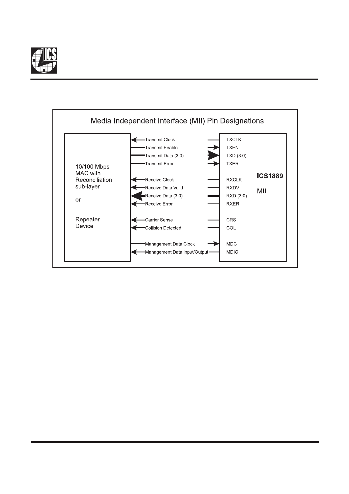
Media Independent Interface (MII)
Station management interface
Extended register set including QuickPollTM detailed
status monitoring
Transmit clock synthesis
Receive clock and data recovery
Detailed receive error reporting
Extended Test Modes
52-pin MQFP package with 2.0 mil body thickness
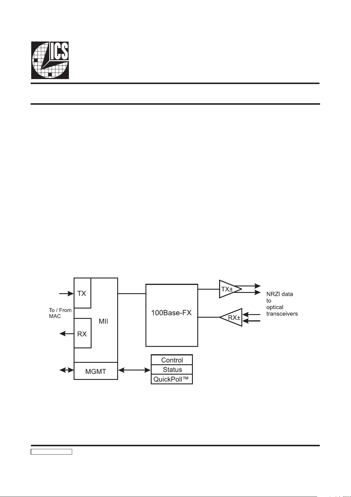
The ICS1889 is a fully integrated physical layer device
supporting 100 Megabits per second CSMA/CD Fast
Ethernet fiber optic applications. It is designed to support
the requirements of DTEs (adapter cards), repeaters and
switches. It is compliant with the ISO/IEC 8802 Fast
Ethernet standard for 100Base-FX. It provides a Media
Independent Interface (MII) allowing direct chip-to-chip
connection, motherboard-to-daughter board connection or
connection via a cable in a similar manner to the AUI
approach used with 10Base-Tsystems. A station
management interface is provided to receive command
information and send status information. It transmits and
receives NRZI data and interfaces directly to the optical
transceiver. It can operate in either half duplex or full
duplex.
Page 2
2
ICS1889
Block Diagram
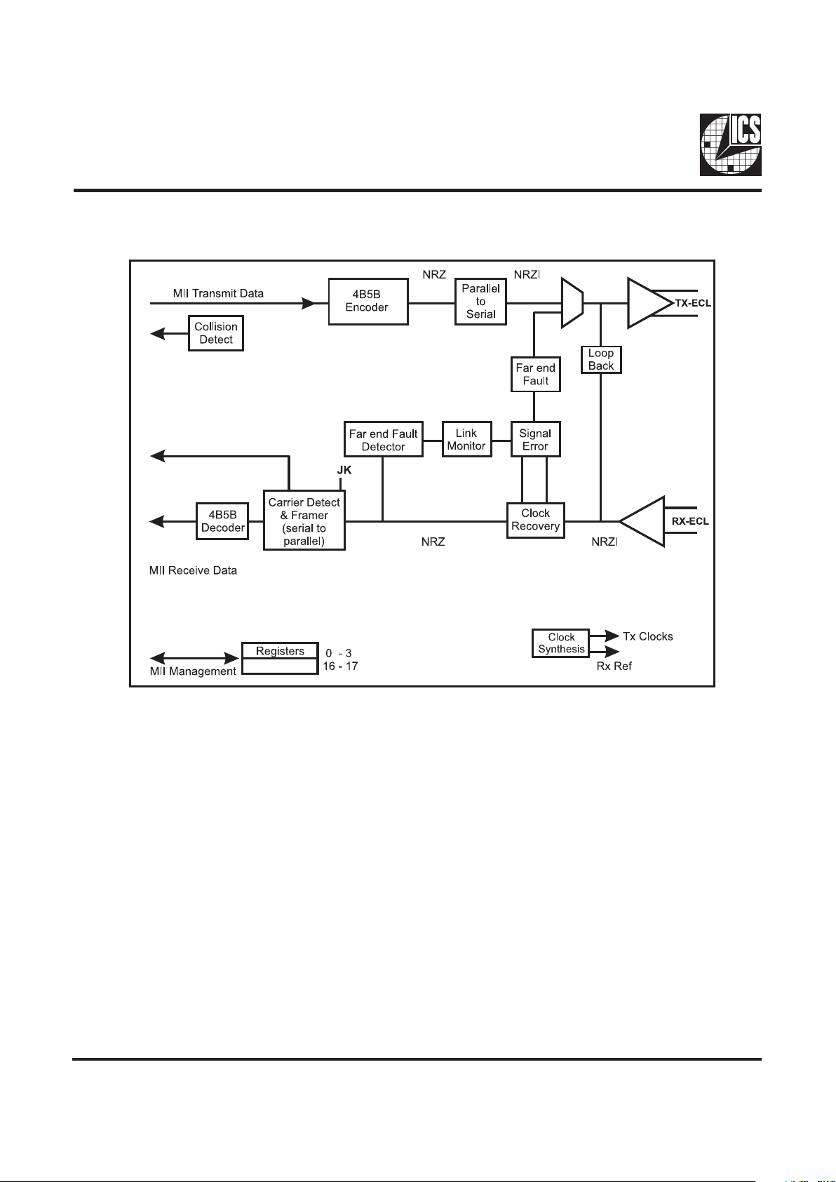
Introduction
The ICS1889 is a nibble to bit stream and bit stream to nibble
processor. When transmitting, it takes sequential nibbles
presented at the Media Independent Interface (MII) and
translates them to a serial bit stream for transmission on the
media. When receiving, it takes the serial bit stream from the
media and translates it to sequential nibbles for presentation
to the MII. It has no knowledge of the underlying structure of
the MAC frame it is conveying.
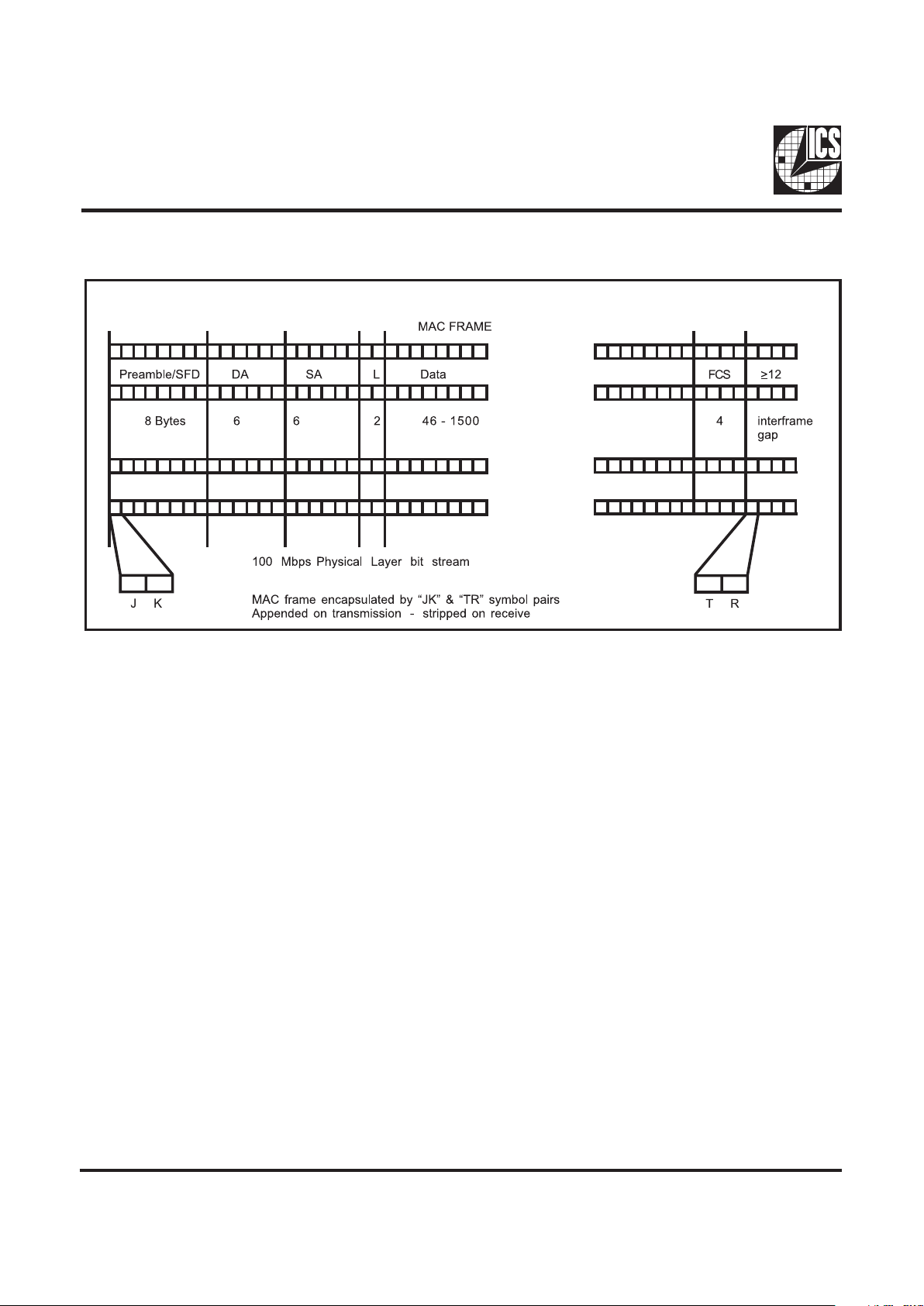
When transmitting, the ICS1889 encapsulates the MAC
frame (including the preamble) with the start-of-stream
(SSD) and end-of-stream (ESD) delimiters. When receiving,
it strips off the SSD and substitutes the normal preamble
pattern and then presents this and subsequent preamble
nibbles to the MII. When it encounters the ESD it ends the
presentation of nibbles to the MII. Thus, the MAC
reconciliation layer sees an exact copy of the transmitted
frame.
During periods when no frames are being transmitted or
received, there is a requirement to signal and detect the idle
condition. This allows the higher levels to determine the
integrity of the connection between the node and the hub. A
continuous stream of ones is transmitted to signify the idle
condition, the receive channel includes logic that monitors
the IDLE data stream to look for this pattern and thereby
establish the link integrity.
Functional Description
Page 3
3
ICS1889
Media Independent Interface (MII)
The ICS1889 implements a fully compliant IEEE 802.3µ
Media Independent Interface for connection to MACs or
repeaters which allows connections between the ICS1889
and MAC on the same board, motherboard/daughter board or
via a cable in a similar manner to AUI connections.
The MII is a specification of signals and protocols which
formalizes the interfacing of a 10/100 Mbps Ethernet Media
Access Controller (MAC) to the underlying physical layer.
The specification is such that different physical media may be
supported (such as 100Base-TX, 100Base-T4 and 100BaseFX) transparently to the MAC.
The MII specifies transmit and receive data paths. Each path
is 4-bits wide allowing for transmission of a nibble or single
symbol. The transmit data path includes a transmit clock for
synchronous transfer, a transmit enable signal and a transmit
error signal. The receive data path includes a receive data
clock for synchronous transfer, a receive data valid signal and
a receive error signal. Both the transmit clock and receive
clock are sourced by the ICS1889. The ICS1889 provides the
MII signals carrier sense and collision detect. In half duplex
mode, carrier sense indicates that data is being transmitted or
received, and in full duplex mode it indicates that data is
being received. Collision detect indicates that data has been
received while a transmission is in progress.
The MII also specifies a two wire interface and a protocol
between station management and the physical layer. The
ICS1889 implements this interface providing a bidirectional
data line and a clock input for synchronizing the data
transfers. This interface allows station management to read
and write all of the ICS1889 registers.
The ICS1889 is designed to allow hot insertion of an MII
cable into the MAC. During the power-up phase, the
ICS1889 will isolate the MII and the transmit pair by
tristating the PHY outputs.
Page 4
4
ICS1889
Transmit Clock Synthesizer
The ICS1889 synthesizes the transmit clock using a PLL to
produce 25 MHz and 125 MHz clocks. This allows the use of
a low cost 25 MHz crystal or a low jitter reference frequency
source.
Receive Clock Recovery
The receive clock recovery logic monitors the receive line and
detects a receive signal. The logic, which includes a PLL,
extracts data and clock from the 100Base-FX, 125 Mbps,
NRZI bit stream. In the event that the PLL is unable to lock on
to the receive signal, it generates a not locked signal. The
transmit clock synthesizer provides a center frequency
reference for operation of the clock recovery circuit in the
absence of data. The receive signal detected and not
locked signals are both used by the logic which monitors the
receive channel for errors.
Carrier Detector & Framer
The carrier detector examines the receive serial bit stream
looking for the SSD, the JK symbol pair. In the idle state,
IDLE symbols (all logic ones) will be received. If the carrier
detector detects a logic zero in the bit stream, it examines the
following bits looking for the first two non-contiguous zeroes,
confirms that the first 5-bits form the J symbol (11000) and
asserts carrier detect. At this point the serial data is framed
and the second symbol is checked to confirm the K symbol
(10001). If successful, the following framed data (symbols)
are presented to the 4B5B decoder. If the JK pair is not
confirmed, the false carrier detect bit is asserted in the
QuickPoll Register and the idle state is reentered.
Page 5
5
ICS1889
4B/5B Encoder/Decoder
The ICS1889 uses a 4B5B coding scheme. This maps a 4-bit
nibble to a 5-bit code group called a symbol. Five bits allow
32 possible symbols, 16 are used for data encoding, 6 are used
for control and 10 are not used and are invalid. The control
symbols used are JK as the SSD, TR as the ESD, I as
the IDLE symbol and H to signal an error. All other
symbols are invalid and, if detected, will set the receive error
bit in the status register, and cause the RXER signal to be
asserted (see Table 1 below).
When transmitting, nibbles from the MII are converted to a 5bit code groups. During transmission, the first 16 nibbles
obtained from the MII are the MAC frame preamble.
The ICS1889 replaces the first two nibbles with the start-ofstream delimiter (the JK symbol pair). Following the last
nibble, the ICS1889 adds the end-of-stream delimiter (the
TR symbol pair).
When receiving, 5-bit code groups are converted to nibbles
and presented to the MII. If the ICS1889 detects one or more
invalid symbols, it sets the Invalid Symbol bit (17:7) in the
QuickPoll Status Register. When receiving a frame, the first
two 5-bit code groups received are the start-of-stream
delimiter (the JK symbol pair), the ICS1889 strips them
and substitutes two nibbles of the normal preamble pattern.
The last two 5-bit code groups are the end-of-stream delimiter
(the TR symbol pair), these are stripped from the nibbles
presented to the MAC.
1. The IDLE symbol is sent continuously between frames.
2. J and K are the SSD and are always sent in pairs.
3. K always follows J.
4. T and R are the ESD and are always sent in pairs.
5. R always follows T.
6. A HALT symbol is used to signal an error condition.
Table 1: 4B5B Encoding
Symbol Meaning
4B Code
3 2 1 0
5B Code
4 3 2 1 0
Symbol Meaning
4B Code
3 2 1 0
5B Code
4 3 2 1 0
0 Data 0 0 0 0 0 1 1 1 1 0 8 Data 8 1 0 0 0 1 0 0 1 0
1 Data 1 0 0 0 1 0 1 0 0 1 9 Data 9 1 0 0 1 1 0 0 1 1
2 Data 2 0 0 1 0 1 0 1 0 0 A Data A 1 0 1 0 1 0 1 1 0
3 Data 3 0 0 1 1 1 0 1 0 1 B Data B 1 0 1 1 1 0 1 1 1
4 Data 4 0 1 0 0 0 1 0 1 0 C Data C 1 1 0 0 1 1 0 1 0
5 Data 5 0 1 0 1 0 1 0 1 1 D Data D 1 1 0 1 1 1 0 1 1
6 Data 6 0 1 1 0 0 1 1 1 0 E Data E 1 1 1 0 1 1 1 0 0
7 Data 7 0 1 1 1 0 1 1 1 1 F Data F 1 1 1 1 1 1 1 0 1
I Idle Undefined 1 1 1 1 1 V Invalid Undefined 0 0 0 1 0
J SSD 0 1 0 1 1 1 0 0 0 V Invalid Undefined 0 0 0 1 1
K SSD 0 1 0 1 1 0 0 0 1 V Invalid Undefined 0 0 1 0 1
T ESD Undefined 0 1 1 0 1 V Invalid Undefined 0 0 1 1 0
R ESD Undefined 0 0 1 1 1 V Invalid Undefined 0 1 0 0 0
H Error Undefined 0 0 1 0 0 V Invalid Undefined 0 1 1 0 0
V Invalid Undefined 0 0 0 0 0 V Invalid Undefined 1 0 0 0 0
V Invalid Undefined 0 0 0 0 1 V Invalid Undefined 1 1 0 0 1
Invalid Error Code Test TXER asserted
I Idle 1 1 1 1 1 1 1 1 1 V Invalid 0 0 1 0 0 0 0 1 0
J SSD 1 1 1 0 1 1 0 0 0 V Invalid 0 0 1 1 0 0 0 1 1
K SSD 1 0 1 1 1 0 0 0 1 V Invalid 0 1 0 1 0 0 1 0 1
T ESD 1 0 0 1 0 1 1 0 1 V Invalid 0 1 1 0 0 0 1 1 0
R ESD 0 1 1 1 0 0 1 1 1 V Invalid 1 0 0 0 0 1 0 0 0
H Error 0 1 0 0 0 0 1 0 0 V Invalid 1 0 1 0 0 1 1 0 0
V Invalid 0 0 0 0 0 0 0 0 0 V Invalid 1 1 0 0 1 0 0 0 0
V Invalid 0 0 0 1 0 0 0 0 1 V Invalid 1 1 0 1 1 1 0 0 1
Page 6
6
ICS1889
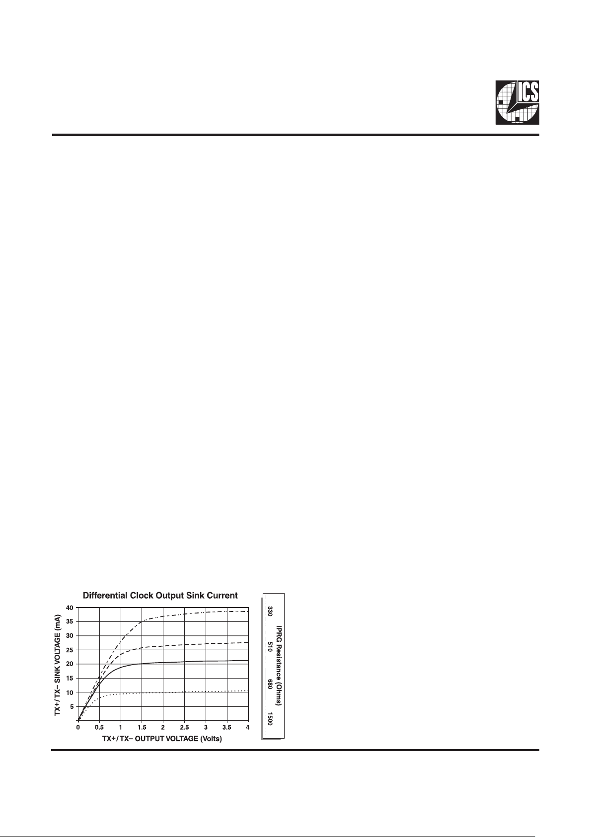
Line Transmitter
The Line Transmitter output pair is a differential positive ECL
(PECL) interface designed to connect directly to a standard
fiber optic transceiver. The differential driver for the transmit
signal is a programmable current source designed for resistive
termination. Using an external resistor connected to the IPRG
pin, the output current may be preset.
The differential driver for the TX ± is current mode and is
designed to drive resistive terminations in a complementary
fashion. The output is current-sinking only, with the amount
of sink current programmable via the IPRG1 pin. The sink
current is equal to four times the IPRG1 current. For most
applications, an 910Ω resistor from VDD to IPRG1 will set
the current to the necessary precision.
The TX± pins are incapable for sourcing current, so V
OH
must
be set by the ratios of the Thevenin termination resistors for
each of the lines. R1 is a pull-up resistor connected from the
PECL output to VDD. R2 is a pull-down resistor connected
from the PECL output to VSS. R1 and R2 are electrically in
parallel from an AC standpoint. If we pick a target impedance
of 50Ω for our transmission line impedance, a value of 62Ω
for R1 and a value of 300Ω for R2 would yield a Thevenin
equivalent characteristic impedance of 49.7Ω and a V
OH
value of VDD -.88 volts, compatible with PECL circuits.
To set a value for VOL, we must determine a value for I
prg
that will cause the output FETs to sink an appropriate current.
We desire VOL to be V
DD
-1.81 or greater. Setting up a sink
current of 19 milliamperes would guarantee this through our
output termination resistors. As this is controlled by
4/1 current mirror, 4.75mA into I
prg
should set this current
properly. A 910Ω resistor from V
DD
to I
prg
should work fine.
Line Receiver
The Line Receiver is a differential input pair designed to
interface directly to a standard fiber optic transceiver. It is a
differential PECL input buffer.
Signal Error Detector
The ICS1889 Signal Error Detector is part of the clock
recovery PLL. It detects a Receive Signal Error if no receive
signal is received and detects a PLL Lock Error if the PLL is
unable to lock on to the receive channel signal. A receive
channel error is defined as the loss of receive signal or the loss
of PLL lock.
Remote Fault Signaling
Remote fault signaling allows a node to indicate receive
channel errors to its Link Partner using its transmit channel.
When used by both nodes on a link segment, the integrity of
both the transmit and receive channels can be verified.
Since 100Base-FX systems do not use auto-negotiation, an
alternative, in-band signaling scheme is used to signal remote
fault conditions. This scheme, Far End Fault Indication, relies
on the characteristics of the quiescent state, (a continuous
IDLE stream). The IDLE stream is a continuous stream of
logic ones and a carrier is defined as the receipt of two
noncontiguous logic zeroes. A Far End Fault is signaled with
84 logic ones followed by one logic zero, with the pattern
repeated at least three times.
A Far End Fault will be signaled under three conditions; the
first is when no activity is received from the Link Partner,
since this can indicate a broken receive wire. The second is
when the clock recovery circuit detects a Receive Signal Error
or PLL Lock Error. The third is when a management entity
sets the Transmit Far End Fault bit (16:3).
Far End Fault signaling continues until the condition causing
the fault ceases.
Far End Fault Detection
The Far End Fault detector monitors the receive data serial bit
stream looking for a repetitive pattern of 84 logic ones
followed by a logic zero. Non-ICS1889 PHYs may have
different definitions of what constitutes a remote fault.
However, an ICS1889 will always respond to the in-band
error signaling scheme. If the ICS1889 detects three
consecutive patterns described above, it will signal a far end
fault to the Link Monitor.
Link Monitor
If the Link Monitor receives a far end fault indication or a
local receive channel error, it causes the ICS1889 to enter the
IDLE mode, isolate the MII and assert the Link Status bit in
the Status Register. Once the far end fault condition is deasserted, the Link Monitor will return to the Link OK
condition if the local receive channel is clear of errors. Once
detected, a receive channel error signal will be indicated from
330 to 1000 microseconds.
Page 7

7
ICS1889
Management Interface
The ICS1889 provides a management interface to connect to
a management entity. The two wire serial interface is part of
the MII and is described in the MII section. The interface
allows the transport of status information from the ICS1889
to the management entity and the transport of command
words to the ICS1889. It includes a register set, a frame
format, and a protocol.
Management Register Set
The register set includes the mandatory basic control and
status registers and an extended set. The ICS1889 implements
the following registers.
Control (register 0)
Status (register 1)
PHY Identifier (register 2)
PHY Identifier (register 3)
Extended Control (register 16)
QuickPoll Status (register 17)
Management Frame Structure
The management interface uses a serial bit stream with a
specified frame structure and protocol as defined below.
Preamble 11...11 (32 ones)
SOF 01
Op Code 10 (read), 01 (write)
Address AAAAA (5 bits)
Register RRRRR (5 bits)
TA NN (2 bits)
Data DD...DD (16 bits)
Idle Zo high impedance
Preamble
The ICS1889 looks for a pattern of 32 logic ones followed by
the SOF delimiter before responding to a transaction.
Start of Frame
Following the preamble a start of frame delimiter of zero-one
initiates a transaction.
Operation Code
The valid codes are 10 for a read operation and 01 for a write
operation. Other codes are ignored.
Address
There may be up to 32 PHYs attached to the MII. This 5 bit
address is compared to the internal address of the ICS1889, as
set by the P[0...4]* pins, for a match.
Register Address
The ICS1889 uses this field to select one of the registers
within the set. If a nonexistent register is specified, the
ICS1889 ignores the command.
TA
This 2-bit field is used by the ICS1889 to avoid contention
during read transactions. When writing to the ICS1889, the
TA bits should be set to 10. When reading from the ICS1889,
the device will tristate during this time.
Data
This is a 16-bit field with bit 15 being the first bit sent or
received.
Idle
The ICS1889 is in the high impedance state during the idle
condition.
Register Access Rules
RO Read Only, writes ignored
CW Command Override Writable
RW/0 Read/Write only logic zero
RW Read/Write
Four types of register access are supported by the device.
Read Only (RO) bits may be read, but writes are ignored.
Command Override Writable (CW) bits may be read, but
writes are ignored unless preceded by writing a logic one to
the Command Register Override bit (16:15). Read Write Zero
(RW/0) bits may be read, but must only be written with a logic
zero value. Writing a logic one to this type of bit may prevent
the device from operating normally. Read Write (RW) bits
may be read and may be written to any value.
Default Values
No default value
0 Default to logic zero
1 Default to logic one
Pin Default depends on the state of
the named pin
Modifier
SC Self Clearing
LL Latching Low
LH Latching High
Self clearing bits will clear without any further writes after a
specified amount of time. Latching bits are used to capture an
event. To obtain the current status of a latching bit, the bit
must be read twice in succession. If the special condition still
persists, the bit will be the same on the second read;
otherwise, the condition indication will not be present.
Page 8
8
ICS1889
Control Register (register 0)
The control register is a 16-bit read/write register used to set
the basic configuration modes of the ICS1889. It is accessed
through the management interface of the MII.
Reset (bit 15) default = 0
Setting this bit to a logic 1 will result in the ICS1889 setting
all its status and control registers to their default values.
During this process the ICS1889 may change internal states
and the states of physical links attached to it. While in process,
the bit will remain set and no other write commands to the
control register will be accepted. The reset process will be
completed within 500 ms and the bit will be cleared indicating
that the reset process is complete.
Loop Back (bit 14)
Setting this bit to a logic one causes the ICS1889 to tristate
the transmit circuitry from sending data and the receive
circuitry from receiving data. The collision detection circuitry
is also disabled unless the collision test command bit is set.
Data presented to the MII transmit data path is returned to the
MII receive data path (see ICS1889 Block Diagram, page 2).
Data Rate (bit 13)
This bit is permanently set to a logic one indicating that only
the 100 Mbps mode is supported.
Auto-Negotiation Enable (bit 12)
This feature is not available with fiber optic solutions. This bit
is permanently set to a logic zero indicating that it is not
supported.
Power-Down (bit 11)
Setting it to logic one will cause the ICS1889 to isolate its
transmit data output and its MII interface with the exception
of the management interface. The ICS1889 will then enter a
power-down mode where only the management interface and
logic remain active. Setting this bit to logic zero after it has
been set to a logic one will cause the ICS1889 to power-up its
logic and then reset all error conditions. It then enables
transmit data and the MII interface. This process takes 500 ms
to complete.
Control Register (register 0)
BIT Function Effect when bit = 0 Effect when bit = 1 Access Default
15
Reset No Effect Reset PHY
RW/S C 0
14
Loop Back Disable loop back mode Enable loop back mode
RW 0
13
Data Rate Always set to a logic one 100 Mpbs operation
RO 1
12
Auto-Negotiate Enable No Effect Alwa ys set to logic zero
RO 0
11
Power-Down Normal Mode Reduced power consumption
RW 0
10
Isolate No Effect Isolate PHY from M II
RW 0 if PHY
Address
< >0,
1 if PHY
Address=0
9
Restart Auto-Negotitation No Effect Alwa ys set to logic zero
RO 0
8
Duplex Mode Half Duplex Full Duplex
RW 0
7
Collision Test No Effect Enable collision signal test
RW 0
6
Reserved
RO 0
5
Reserved
RO 0
4
Reserved
If read, bits 0-6 and bits 9 and 12 wi ll return logic
zeroes and bit 13 will return a logic one.
RO 0
3 RO 0
2
Reserved Writes to these bits will have no effect.
RO 0
1
Reserved
RO 0
0
Reserved
RO 0
Page 9

9
ICS1889
Isolate (bit 10)
Setting this bit to a logic one causes the ICS1889 to isolate its
data paths from the MII. In this mode, sourced signals
(TXCLK, RXCLK, RXDV, RXER, RXD0-3, COL and CRS)
are in a high impedance state and input signals (TXD0-3,
TXEN and TXER) are ignored. The management interface is
unaffected by this command.
When the PHY address is set to 0, the device will power-up in
the isolated mode (bit 10=1). For all other addresses, the
default will be bit 10=0.
Restart Auto-Negotiation (bit 9)
This feature is not available with fiber optic solutions. This
bit is permanently set to a logic zero indicating that it is not
supported.
Duplex Mode (bit 8)
Setting this bit to a logic one causes the ICS1889 to operate in
the full duplex mode and setting this bit to a logic zero causes
it to operate in the half duplex mode. If the ICS1889 is
operating in loop back mode, this bit will have no effect on
the operation.
Collision Test (bit 7)
This command bit is used to test that the collision circuitry is
working when the ICS1889 is operating in the loop back
mode. Setting this bit to a logic one causes the ICS1889 to
assert the collision signal within 512 bit times of TXEN being
asserted and to de-assert it within 4-bit times of TXEN being
de-asserted. Setting this bit to a logic zero causes the
ICS1889 to operate in the normal mode.
Reserved (Bits 6 through 0)
These bits are reserved for future IEEE standards. When read,
logic zeroes are returned. Writing has no effect on ICS1889
operation.
Page 10

10
ICS1889
Status Register (register 1)
The ICS1889 status register is a 16 bit read only register
used to indicate the basic status of the ICS1889. It is
accessed via the management interface of the MII. It is
initialized during a power-up or reset to predefined default
values. If the ICS1889 is enabled for auto-configuration,
certain bits in the status register may be set to zero as defined
below.
100Base-T4 (bit 15)
This bit is permanently set to a logic zero indicating that the
ICS1889 is not able to support 100Base-T4 operation.
100Base-X Full Duplex (bit 14)
This bit defaults to a logic one indicating that the ICS1889 is
able to support 100Base-X Full Duplex operation.
100Base-X Half Duplex (bit 13)
This bit defaults to a logic one indicating that the ICS1889 is
able to support 100Base-X Half Duplex operation.
10 Mbps Full Duplex (bit 12)
This bit is permanently set to a logic zero indicating that
10Base-T is not supported.
10 Mbps Half Duplex (bit 11)
This bit is permanently set to a logic zero indicating that
10Base-T is not supported.
Reserved (bits 10 through 6)
These bits are reserved for future IEEE standards. When read,
logic zeroes are returned. Writing has no effect on ICS1889
operation.
Auto-Negotiation Complete (bit 5)
This bit is permanently set to a logic zero.
Remote Fault (bit 4)
When set to a logic one, this bit indicates that a remote fault
(Far End Fault) has been detected by the Link Monitor. This
bit remains set to a logic one until it is cleared by reading the
status register or by a reset command
If the link partner is implemented with a non-ICS1889 device,
the causes of a link failure will be specified by that PHY
vendor. If the link partner is implemented with an ICS1889, a
remote fault indication means a receive channel error
occurred.
Auto-Negotiation Ability (bit 3)
This feature is not available with fiber optic solutions. This bit
is permanently set to a logic zero indicating that it is not
supported.
Control Register (register 1)
BIT Definition When bit = 0 When bit = 1 Access Default
15 OUI bit 19 | s CW 0
14 OUI bit 20 | t CW 1
13 OUI bit 21 | u CW 1
12 OUI bit 22 | v CW 0
11 OUI bit 23 | w CW 0
10 OUI bit 24 | x CW 0
9 Manufacturer’s Model Number bit 5 CW 0
8 Manufacturer’s Model Number bit 4 CW 0
7 Manufacturer’s Model Number bit 3 CW 0
6 Manufacturer’s Model Number bit 2 CW 0
5 Manufacturer’s Model Number bit 1 CW 0
4 Manufacturer’s Model Number bit 0 CW 1
3 Revision Number bit 3 CW 0
2 Revision Number bit 2 CW 1
1 Revision Number bit 1 CW 0
0 Revision Number bit 0 CW 1
Page 11

11
ICS1889
Link Status (bit 2)
When set to a logic one, this bit indicates that the Link
Monitor has established a valid link. If the Link Monitor
detects a link failure, this bit is set to a logic zero and remains
zero through the next read of the status register. A link failure
may be due to an error in the receive channel or an error in the
receive channel of the link partner (that is, a remote fault).
Jabber detect (bit 1)
This bit is permanently set to a logic zero.
Extended Capability (bit 0)
This bit is permanently set to a logic one indicating that the
ICS1889 has an extended register set.
Page 12

12
ICS1889
PHY Identifier Register (register 2)
Register 2 and Register 3 contain the 24-bit Organizationally
Unique Identifier (OUI), Manufacturers Model Number and
Revision Number. Integrated Circuit Systemss OUI is used as
the default for registers 2 and 3. These values may be
overridden using the Command Override bit (16:15).
Organizationally Unique Identifier
bits 3-18(bits 15-0)
This field contains the lowest 16 bits of the IEEE OUI
excluding bits 0, 1, and 2. Bit 3 of the OUI maps to bit 15 of
the register.
OUI Formatting Information
The ICS OUI is shown below with information on mapping
the OUI value into registers 2 and 3.
Octet Format:
00 A0 BE
| | Third octet
| Second octet
First octet
Binary Format:
0 0 0 A E B
0000 0000 0000 0101 0111 1101
lsb msb lsb msb lsb msb
(I/G)
IEEE Standard 802 Lettered Format
0000 0000 0000 0101 0111 1101
abcd efgh ijkl mnop qrst uvwx
Model and Revision Information
Model Part
1 ICS1889
2 ICS1890
The revision number will be incremented each time the silicon
is significantly revised.
These two registers can always be read and may be written by
setting the Command Override bit in the Configuration
register (16:15) and then performing a write operation. At
power-up and reset they are set to Integrated Circuit
Systemss OUI. By allowing these registers to be written, a
systems vendor may substitute their own OUI.
PHY Identifier Register (register 2)
BIT Definition When bit = 0 When bit = 1 Access Default
15 OUI bit 3 | c CW 0
14 OUI bit 4 | d CW 1
13 OUI bit 5 | e CW 1
12 OUI bit 6 | f CW 0
11 OUI bit 7 | g CW 0
10 OUI bit 8 | h CW 0
9 OUI bit 9 | i CW 0
8 OUI bit 10 | j CW 0
7 OUI bit 11 | k CW 0
6 OUI bit 12 | l CW 0
5 OUI bit 13 | m CW 0
4 OUI bit 14 | n CW 1
3 OUI bit 15 | o CW 0
2 OUI bit 16 | p CW 1
1 OUI bit 17 | q CW 0
0 OUI bit 18 | r CW 1
Page 13

13
ICS1889
PHY Identifier Register (register 3)
Register 2 and Register 3 contain the 24 bit Organizationally
Unique Identifier (OUI), Manufacturers Model Number and
Revision Number. Integrated Circuit Systemss OUI is used as
the default for registers 2 and 3.
These two registers can always be read and may be written by
setting the Command Override bit in the Configuration
register (16:15) and then performing a write operation. At
power-up and reset they are set to Integrated Circuit Systems
OUI. By allowing these registers to be written, a systems
vendor may substitute their own OUI.
See register 2 for OUI formatting information.
Organizationally Unique Identifier
bits 19-24 (bits 15-10)
This field contains the upper 6 bits of the IEEE OUI. Bit 19 of
the OUI maps to bit 15 of the register.
Manufacturers Model Number bits 5-0 (bits 9-4)
Model Part
1 ICS1889
2 ICS1890
Revision Number bits 3-0 (bits 3-0)
The revision number will be incremented each time the silicon
is significantly revised. Currently the device is at revision 1.
PHY Identifier Register (register 3)
BIT Definition When bit = 0 When bit = 1 Access Default
15 OUI bit 19 | s CW 0
14 OUI bit 20 | t CW 1
13 OUI bit 21 | u CW 1
12 OUI bit 22 | v CW 0
11 OUI bit 23 | w CW 0
10 OUI bit 24 | x CW 0
9 Manufacturer’s Model Number bit 5 CW 0
8 Manufacturer’s Model Number bit 4 CW 0
7 Manufacturer’s Model Number bit 3 CW 0
6 Manufacturer’s Model Number bit 2 CW 0
5 Manufacturer’s Model Number bit 1 CW 0
4 Manufacturer’s Model Number bit 0 CW 1
3 Revision Number bit 3 CW 0
2 Revision Number bit 2 CW 1
1 Revision Number bit 1 CW 0
0 Revision Number bit 0 CW 1
Page 14

14
ICS1889
Extended Control Register (register 16)
The Extended Control Register is a 16-bit read write register
used to pre-program the ICS1889. At power-up and reset, this
register will be loaded to the default values specified. It may
subsequently be read or written. If written, the result is bit
dependent as discussed below.
Command Register Override (bit 15)
If set to a logic one, this bit allows a subsequent write to the
Status Register (register 1) and the PHY identifier registers 2
and 3. The contents of registers 2 and 3 may be set to any
value. The Status Register may have certain specified bits set
or reset. The first write to registers 1, 2 or 3 after this bit is set
will reset it preventing subsequent writes from having any
effect.
Reserved (bit 14)
This bit is reserved for ICS use. It must always be written with
a logic zero. The value of this bit when read is unspecified and
may be a logic zero or one.
Reserved (bit 13)
This bit is reserved for ICS use. It must always be written with
a logic zero. The value of this bit, when read, is unspecified
and may be a logic zero or one.
Extended Control Register (register 16)
BIT Definition When bit = 0 When bit = 1 Access Default
15 Command Register Override Don’t allow write Allow write RW 0
14 Reserved for ICS Write logic zero. Read unspecified. RW/0 —
13 Reserved for ICS Write logic zero. Read unspecified. RW/0 —
12 Reserved for ICS Write logic zero. Read unspecified. RW/0 —
11 Reserved for ICS Write logic zero. Read unspecified. RW/0 —
10 PHY address - S4 CW P4RD
9 PHY address - S3 MII management CW P3TD
8 PHY address - S2 Register address code CW P2LI
7 PHY address - S1 0 - 31 Read Only CW P1CL
6 PHY address - S0 CW P0FD
5 Reserved for ICS Write logic zero. Read unspecified. RW/0 —
4 Far End Fault Disabled Enabled RW 1
3 Transmit Far End Fault No fault transmitted Fault transmitted RW 0
2 Invalid Error Code Test Disabled Enabled RW 0
1 Reserved for ICS Write logic zero. Read unspecified. RW/0 —
0 Reserved for ICS Write logic zero. Read unspecified. RW/0 —
Reserved (bit 12)
This bit is reserved for ICS use. It must always be written with
a logic zero. The value of this bit when read is unspecified and
may be a logic zero or one.
Reserved (bit 11)
This bit is reserved for ICS use. It must always be written with
a logic zero. The value of this bit when read is unspecified and
may be a logic zero or one.
PHY Address (Bits 10 through 6)
These 5 bits are used to indicate the address of the ICS1889
on the management port of the MII (any number in the range
0 - 31). A read returns the address. Extra care should be taken
if a command override write is performed on these bits, as a
change in the PHY address must be accounted for by the
device reading and writing to the MII Management interface.
Reserved (bit 5)
This bit is reserved for ICS use. It must always be written with
a logic zero. The value of this bit when read is unspecified and
may be a logic zero or one.
Page 15

15
ICS1889
Enable Far End Fault (bit 4)
If this bit is set to a logic one, the far end fault logic becomes
active resulting in faults being signaled and recognized via the
in-band signaling scheme. If this bit is set to a logic zero,
the far end fault logic is disabled.
Transmit Far End Fault (bit 3)
Management may indicate a fault has occurred to its link
partner by setting this bit to a logic one. Indicating a fault
brings the link down and disables the reception of data until
this bit is cleared and the link is reestablished.
Invalid Error Code Test (bit 2)
If this bit is set to a logic one, the 4B5B encoder operates as a
5B5B encoder obtaining the fifth bit of the code group from
the value of TXER.
Reserved (bit 1)
This bit is reserved for ICS use. It must always be written with
a logic zero. A read always returns a logic zero.
Reserved (bit 0)
This bit is reserved for ICS use. It must always be written with
a logic zero. A read always returns a logic zero.
Page 16

16
ICS1889
QuickPoll Status Register (register 17)
The QuickPoll status register is a 16-bit read only register
used to indicate the comprehensive status of the ICS1889. All
register status bits that might need to be repetitively examined
at run time are located in this register, even though some bits
duplicate functionality from other registers. This allows the
device status to be rapidly obtained with a single register
access.
The register is accessed via the management interface of the
MII. It can always be read and may be written by setting the
override bit in the Configuration Register (register 16, bit 15)
and then performing a write operation. It is initialized during a
power-up or reset to predefined default values.
QuickPoll Status Register (register 17)
BIT Definition When bit = 0 When bit = 1 Access Default
15 Data Rate Always a logic one 100 Mbps selected RO 1
14 Duplex Half duplex selected Full duplex selected RO
0 if PRIO=1 or
DPEN if PRIO=0
13 Reserved for ICS Read unspecified RO —
12 Reserved for ICS Read unspecified RO —
11 Reserved for ICS Read unspecified RO —
10 Receive Signal Error Signal Loss of signal RO/LH 0
9 PLL Lock Error PLL locked PLL failed to lock RO/LH 0
8 False Carrier Detect Normal carrier or idle False carrier detected RO/LH 0
7 Invalid Symbol Valid symbols Invalid symbol detected RO/LH 0
6 Halt Symbol Normal symbols HALT symbol detected RO/LH 0
5 Premature End Normal stream Stream with two IDLES RO/LH 0
4 Reserved for ICS Read unspecified RO —
3 Reserved for ICS Read unspecified RO —
2 Priority Pin State Hardware Software RO PRIO
1 Remote Fault No remote fault detected Remote fault detected RO/LH 0
0 Link Status Link is not valid Link is valid RO/LL 0
Page 17

17
ICS1889
Data Rate (bit 15)
This bit is permanently set to a logic one indicating it only
operates at 100 Mbps.
Duplex (bit 14)
If set to a logic one, this bit indicates that the full duplex mode
has been selected. If set to a logic zero, it indicates that the
half duplex mode has been selected. It is initialized to logic
zero.
Reserved (bit 13)
This bit is reserved for ICS use. The value of this bit is
unspecified and may be a logic zero or one.
Reserved (bit 12)
This bit is reserved for ICS use. The value of this bit is
unspecified and may be a logic zero or one.
Reserved (bit 11)
This bit is reserved for ICS use. The value of this bit is
unspecified and may be a logic zero or one.
Receive Signal Error (bit 10)
If set to a logic one, the Receive Signal error bit indicates that
the ICS1889 read channel has at some point been unable to
detect the receive channel signal. This bit will remain set until
cleared by reading the contents of register 17. It is initialized
to logic zero.
PLL Lock Error (bit 9)
If set to a logic one, the loss of PLL lock (bit 9) indicates that
the ICS1889 read channel PLL has failed to lock on to the
read channel signal. This bit will remain set until cleared by
reading the contents of register 17. It is initialized to logic
zero.
False Carrier (bit 8)
If set to a logic one, the false carrier (bit 8) indicates that the
ICS1889 has detected a false carrier sometime since this bit
was last reset. This bit will remain set until cleared by reading
the contents of register 17. It is initialized to logic zero.
Invalid Symbol (bit 7)
If set to a logic one, the invalid symbol (bit 7) indicates that an
invalid symbol has been detected in a received frame since the
bit was last reset. This bit will remain set until cleared by
reading the contents of register 17. It is initialized to logic
zero.
Halt Symbol (bit 6)
If set to a logic one, the halt symbol (bit 6) indicates that the
ICS1889 has detected the halt symbol in a frame since bit 11
was last reset. This bit will remain set until cleared by reading
the contents of register 17. It is initialized to logic zero.
Premature End (bit 5)
This bit is normally a logic zero indicating normal data
streams. If two IDLE symbols are detected during the
reception of a receive data stream, this bit is set to a logic one
and the ICS1889 returns to the idle state This bit is initialized
to a logic zero.
Reserved (bit 4)
This bit is reserved for ICS use. The value of this bit is
unspecified and may be a logic zero or one.
Reserved (bit 3)
This bit is reserved for ICS use. The value of this bit is
unspecified and may be a logic zero or one.
Priority Pin State (bit 2)
This bit reflects the setting of the Priority Pin (pin 17). When
this bit is a logic zero, duplex mode is controlled by the
Duplex Enable pin (pin 18). When this bit is a logic one,
duplex mode is controlled by the Duplex Mode bit (0:8).
Remote Fault (bit 1)
This is a copy of the Remote Fault bit of the Status Register
(register 1).
Link Status (bit 0)
This is a copy of the Link Status bit of the Status Register
(register 1).
Page 18

18
ICS1889
Pin Definitions
MII Interface Pin Descriptions
Transmit Clock TXCLK
The Transmit Clock (TXCLK) is a continuous clock signal
generated by the ICS1889 to synchronize the Transmit
Enable, Transmit Data and Transmit Error lines. The
ICS1889 clock frequency is 25% of the nominal transmit data
rate. At 100 Mbps its frequency is 25 MHz. The TXCLK
clock duty cycle is in the range 35% to 65%.
Transmit Enable TXEN
Transmit Enable (TXEN) indicates to the ICS1889 that the
MAC is sending valid data nibbles for transmission on the
physical media. Synchronous with its assertion the ICS1889
will begin reading the data nibbles on the transmit data lines.
It is the responsibility of the MAC to order the nibbles so that
the preamble is sent first, followed by destination, source,
length, data and CFS fields since the ICS1889 has no
knowledge of the frame structure and is merely a nibble
processor. The ICS1889 terminates transmission of nibbles
following the deassertion of Transmit Enable (TXEN).
Transmit Data 3 TXD3
Transmit Data 3 (TXD3) is the most significant bit of the
transmit data nibble. TXD3 is sampled by the ICS1889
synchronously with the Transmit Data Clock when TXEN is
asserted. When TXEN is de-asserted the ICS1889 is
unaffected by the state of TXD3
Transmit Data 2 TXD2
Transmit Data 2 (TXD2) is sampled by the ICS1889
synchronously with the Transmit Data Clock when TXEN is
asserted. When TXEN is de-asserted the ICS1889 is
unaffected by the state of TXD2.
Transmit Data 1 TXD1
Transmit Data 1 (TXD1) is sampled by the ICS1889
synchronously with the Transmit Data Clock when TXEN is
asserted. When TXEN is de-asserted the ICS1889 is
unaffected by the state of TXD1.
Signal Meaning Signal Meaning
TXCLK Transmit Clock TX+ Transmitted data positive
TXEN Transmit Enable TX– Transmitted Data negative
TXD3 Transmit Data 3 IPRG Current program
TXD2 Transmit Data 2 RX+ Receive Data positive
TXD1 Transmit Data 1 RX– Receive Data negative
TXD0 Transmit Data 0 REF+ Frequency reference
TXER Transmit Error REF– Frequency reference
RXCLK Receive Clock SD+ Signal Detect
RXDV Receive Data Valid SD– Signal Detect
RXD3 Receive Data 3
RXD2 Receive Data 2 SYSR System reset
RXD1 Receive Data 1 PRIO Priority
RXD0 Receive Data 0 DPEN Duplex Enable
RXER Receive Error LSTA Link Status
CRS Carrier Sense P4RD Receive data LED
COL Collision Detect P3TD Transmit data LED
P2LI Link Integrity LED
MDC Management Data Clock P1CL Collision detect LED
MDIO Management Data Input/Output P0FD Full duplex LED
NOD/REP Node or Repeater Mode Selection
Page 19

19
ICS1889
Transmit Data 0 TXD0
Transmit Data 0 (TXD0) is the least significant bit of the
transmit data nibble. TXD0 is sampled by the ICS1889
synchronously with the Transmit Data Clock when TXEN is
asserted. When TXEN is de-asserted the ICS1889 is
unaffected by the state of TXD0.
Transmit Error TXER
The assertion of Transmit Error (TXER) for one or more clock
periods will cause the ICS1889 to emit one or more HALT
symbols. The signal is synchronous with TXCLK. In the
normal operating mode, a HALT symbol will be substituted
for the next nibble encoded. If the invalid error code test bit in
the Configuration Register is set (register 16, bit 2), TXER
becomes an additional input to the 4B5B encoder. This allows
the ICS1889 to send the full set of 32 symbols including the
invalid symbols. Table 1 shows the modified 4B5B encoding
in the test mode. A timing diagram for TXER is shown in
Figure xxx.
Receive Clock RXCLK
The Receive Clock (RXCLK) is sourced by the ICS1889.
There are two possible sources for the Receive Clock
(RXCLK). When a carrier is present on the receive pair, the
source is the recovered clock from the data stream. When no
carrier is present on the receive pair, the source is
synchronized to the transmit PLL. The IDLE symbol is sent
during periods of inactivity and the Recovered clock will be
selected.
The ICS1889 will only switch between clock sources when
Receive Data Valid (RXDV) is de-asserted. During the period
between Carrier Sense (CRS) being asserted and Receive
Data Valid being asserted, a clock phase change of up to 360
degrees may occur. Following the de-assertion of Receive
Data Valid a clock phase of 360 degrees may occur.
When Receive Data Valid is asserted, the Receive Clock
frequency is 25% of the data rate, 25 MHz. The minimum low
and high times of the clock are guaranteed to be 35% under all
conditions and the duty cycle between 35% and 65% except
during the clock transition conditions specified above. The
ICS1889 synchronizes Receive Data Valid, Received Data
and Receive Error with Receive Clock (RXCLK).
Receive Data Valid RXDV
Receive Data Valid (RXDV) is generated by the ICS1889. It
indicates that the ICS1889 is recovering and decoding data
nibbles on the Receive Data (RXD) data lines synchronous
with the Receive Data Clock (RXCLK). It is the responsibility
of the MAC to assemble nibbles into MAC frames since the
ICS1889 has no knowledge of the frame structure and is
merely a nibble processor. The ICS1889 asserts RXDV
when it detects a start of stream delimiter (SSD) and deasserts it following the last data nibble or upon detection of a
signal error. RXDV is synchronous with the Receive Data
Clock (RXCLK).
Receive Data RXD3
Receive Data 3 (RXD3) is the most significant bit of the
receive data nibble. RXD is sourced by the ICS1889. When
Receive Data Valid (RXDV) is asserted by the ICS1889, it
will transfer the fourth bit of the symbol synchronously with
Receive Clock (RXCLK).
Receive Data RXD2
Receive Data 2 (RXD2) is sourced by the ICS1889. When
Receive Data Valid (RXDV) is asserted by the ICS1889, it
will transfer the third bit of the symbol synchronously with
Receive Clock (RXCLK).
Receive Data RXD1
Receive Data 1 (RXD1) is sourced by the ICS1889. When
Receive Data Valid (RXDV) is asserted by the ICS1889, it
will transfer the second bit of the symbol synchronously with
Receive Clock (RXCLK).
Receive Data RXD0
Receive Data 0 (RXD0) is the least significant bit of the
receive data nibble. RXD0 is sourced by the ICS1889. When
Receive Data Valid (RXDV) is asserted by the ICS1889, it
will transfer the first bit of the symbol synchronously with
Receive Clock (RXCLK).
Page 20

20
ICS1889
Receive Error (RXER)
The ICS1889 detects two types of receive errors, errors
occurring during the reception of valid frames and an error
condition known as false carrier detect. False carrier detect is
signaled so that repeater applications can prevent the
propagation of false carrier detection. RXER always
transitions synchronously with RXCLK.
The assertion of Receive Error (RXER) for one or more clock
periods during the period when RXDV is asserted (receiving
a frame) indicates that the ICS1889 has detected a read
channel error. There are three sources of read channel error
loss of receive signal, failure of the PLL to lock and invalid
symbol detection (including the HALT symbol). Timing
diagram xxx (RXER Timing Diagram) shows the relationship
of RXER to RXCLK, RXEN and receive channel error
conditions.
RXER may also be asserted when RXDV is de-asserted. The
ICS1889 will assert RXER and set RXD(3:0) to 1110 if a
false carrier is detected. For a good carrier to be detected, the
ICS1889 looks continuously at the incoming IDLE stream
(1111...) for two non-contiguous logic zeros and then checks
for the SSD of JK. In the event that two non-contiguous
logic zeroes are detected but the JK symbol pair is not, then a
false carrier condition is signaled and the IDLE condition is
reentered.
Carrier Sense (CRS)
The ICS1889 asserts Carrier Sense (CRS) when it detects that
receive channel is non-idle in the full duplex mode or when it
detects that either the receive or transmit channels are nonidle in the half duplex mode. A receive channel non-idle
condition is detected by two non-contiguous zeros in any 10
bits (IJ). CRS is not synchronous to either the transmit or
receive clocks.
Collision Detected (COL)
The ICS1889 asserts Collision Detected (COL) when it
detects a receive carrier (non-idle) condition while
transmitting (TXEN asserted) in the half duplex mode. The
COL is not synchronous to either the transmit or receive
clocks. In full duplex mode, collision will be disabled.
Management Data Clock (MDC)
The Management Data Clock (MDC) is used by the ICS1889
to synchronize the transfer of management information to or
from the ICS1889. The ICS1889 requires minimum high and
low times of 160 ns and a minimum clock period of 400 ns.
Management Data Input/Output
The Management Data Input/Output (MDIO) is a tristate line
driven by station management to transfer command
information or driven by the ICS1889 to transfer status
information. All transfers and sampling are synchronous with
MDC. If the ICS1889 is to be used in an application which
uses the mechanical MII specification, MDIO must have a
pull-up at the ICS1889 end and a pull-down at the station
management end. This enables station management to
determine if the connection is intact.
Transmit and Receive Pin Descriptions
Transmit Pair (TX+ & TX-)
The Transmit pair TX+ and TX- carries the NRZI serial bit
stream for conversion to optical signals.
Receive Pair (RX+ & RX-)
The Receive pair RX+ and RX- carries the NRZI serial bit
stream from the optical converter.
Transmit Current Program (IPRG)
This pin is connected to a resistor and sets the current drive of
the transmitter.
Frequency Reference (REF_IN and REF_OUT)
A 25 MHz crystal oscillator or reference source should be fed
into the REF_IN input, while leaving REF-OUT not
connected.
Signal Detect (SD+ & SD-)
This PECL input pair provides a signal detect indication from
the optical transceiver. The ICS1889 will indicate a receive
channel error if this signal is de-asserted. A receive channel
error is also indicated if either a PLL lock error or a receive
signal error is detected.
Page 21

21
ICS1889
Initialization & LED Pin Descriptions
A set of five pins is dual purpose. At power-up and reset they
define the MII PHY address of this ICS1889. Subsequent to
power-up and reset, they become LED status indicators. The
five pins are used to set the PHY address by connecting them
to Vss to indicate a logic one and ground to indicate a logic
zero. They must be connected to either Vss or ground using an
LED (see Figure xxx). At power-up or reset, the ICS1889 will
determine weather the pin is tied to ground or Vss and set the
appropriate value in the configuration register. It will then
determine the polarity of the signal required to drive the LED
and enter the status indicating mode. It will stay in this state
until a reset occurs.
PHY Address 4 - Receive Data LED (P4RD)
At power-up and reset this pin is sampled for a logic high or
zero. If a logic one is detected, a value of 16 is set in the
configuration register.
The ICS1889 sets this bit to the appropriate value to turn on
the LED when receive data is detected. This signal is sticky
and will ensure that a single packet will be seen. If the packet
stream is continuous, the LED will appear permanently on.
PHY Address 3 - Transmit Data LED (P3TD)
At power-up and reset this pin is sampled for a logic high or
zero. If a logic one is detected, a value of 8 is set in the
configuration register.
The ICS1889 sets this bit to the appropriate value to turn on
the LED when transmit data is detected. This signal is sticky
and will ensure that a single packet will be seen. If the packet
stream is continuous, the LED will appear permanently on.
PHY Address 2 - Link Integrity LED (P2LI)
At power-up and reset this pin is sampled for a logic high or
zero. If a logic one is detected, a value of 4 is set in the
configuration register.
The ICS1889 sets this bit to the appropriate value to turn on
the LED when the Link Integrity status is OK.
PHY Address 1 - Collision LED (P1CL)
At power-up and reset this pin is sampled for a logic high or
zero. If a logic one is detected, a value of 2 is set in the
configuration register.
The ICS1889 sets this bit to the appropriate value to turn on
the LED when a collision is detected. This signal is sticky and
will ensure that a single collision will be seen. If the collisions
are continuous, the LED will appear permanently on.
PHY Address 0 - Full Duplex LED (P0FD)
At power-up and reset this pin is sampled for a logic high or
zero. If a logic one is detected, a value of 1 is set in the
configuration register.
The ICS1889 sets this bit to the appropriate value to turn on
the LED when the Full Duplex mode is selected.
Priority (PRIO)
When connected to ground, this pin enables the Duplex
Enable Pin (DPEN) to select the duplex mode. When this pin
is high, DPEN becomes an output indicating the duplex mode
selected.
Duplex Enable (DPEN)
If the Priority pin (PRIO) is high, Duplex Enable (DPEN) is
an output indicating the selected duplex mode. A logic one
indicates full duplex and a logic zero indicates half duplex. If
the Priority Pin is grounded, this pin becomes an input that
sets the duplex mode, a logic one setting the full duplex mode
and a logic zero setting the half duplex mode.
Link Status (LSTA)
This signal indicates the status of the link monitor. A logic one
indicates that the link integrity is OK.
System Reset (SYSR)
When grounded for more than 80ns, this pin causes the
ICS1889 to enter a reset cycle. Upon completion of a reset, the
ICS1889 will be initialized to the same state as that following a
power-up cycle. If SYSR is held low, the ICS1889 remains in
the reset state.
Node/Repeater (NOD/REP)
When this input is logic zero, the device will default to Node
operation. SQE test will default to on.
When this input is logic one, the device will default to
Repeater operation. SQE test will default to off and Carrier
Sense will be determined by receive activity only.
The NOD/REP pin does not have a default configuration and
must be tied either to ground or supply.
Page 22

22
ICS1889
PIN Signal Meaning PIN Signal Meaning
1 VDD VDD (LEDs) 27 RXD1 Receive Data 1
2 NOD/REP Node or Repeater Mode Selection 28 RXD0 Receive Data 0
3 TX– Transmitted Data negative 29 RXDV Receive Data Valid
4 TX+ Transmitted Data positive 30 RXCLK Receive Clock
5 IPRG Current program 31 RXER Receive Error
6 VSS VSS (Transmit Data) 32 VSS VSS (MII I/O)
7 VSS VSS 33 VDD VDD (MII I/O)
8 RX+ Receive Data positive 34 TXER Transmit Error
9 RX– Receive Data negative 35 TXCLK Transmit Clock
10 SD+ Signal Detect 36 TXEN Transmit Enable
11 SD– Signal Detect 37 TXD0 Transmit Data 0
12 N/C No Connect 38 TXD1 Transmit Data 1
13 N/C No Connect 39 TXD2 Transmit Data 2
14 VDD VDD (Receive) 40 TXD3 Transmit Data 3
15 LSTA Link Status 41 COL Collision Detect
16 SYSR System reset 42 CRS Carrier Sense
17 PRIO Priority 43 VSS VSS (Transmit)
18 DPEN Duplex Enable 44 REF_OUT Frequency reference out
19 N/C No Connect 45 REF_IN Frequency reference in
20 N/C No Connect 46 VDD VDD (Transmit)
21 N/C No Connect 47 VSS VSS (LEDs)
22 VSS VSS (Receive) 48 P0FD Full duplex LED
23 MDIO Management Data Input/Output 49 P1CL Collision detect LED
24 MDC Management Data Clock 50 P2LI Link Integrity LED
25 RXD3 Receive Data 3 51 P3TD Transmit data LED
26 RXD2 Receive Data 2 52 P4RD Receive data LED
Pin Assignments
Packaging
Pin Diagram
Page 23

23
ICS1889
System Diagram
Page 24

24
ICS1889
Absolute Maximum Ratings
VDD (measured to VSS) . . . . . . . . . . . . . . . . . 7.0 V
Digital Inputs/Outputs . . . . . . . . . . . . . . . . . V
SS
0.5 V to VDD +0.5 V
Ambient Operating Temperature . . . . . . . . . 55°C to +125° C
Storage Temperature . . . . . . . . . . . . . . . . . . . 65°C to +15 0° C
Junction Temperature . . . . . . . . . . . . . . . . . . 175°C
Soldering Temperature . . . . . . . . . . . . . . . . . 265°C
Recommended Operating Conditions
Stresses above those listed under Absolute Maximum Ratings above may cause permanent damage to the device. This is a stress
rating only and functional operation of the device at these or any other conditions above those listed in the operational sections
of the specifications is not implied. Exposure to absolute maximum rating conditions for extended periods may affect product
reliability.
PARAMETER SYM BOL TEST CONDITIONS MIN MAX UNITS
Ambient Operating Temp. T
A 0+70ºC
Using a Positive Supply V
SS
VDD
0.0
+4.75
0.0
+5.25
V
V
Page 25

25
ICS1889
VDD = V
MIN
to V
MAX
, VSS = 0V, TA = T
MIN
to T
MAX
Note: REF_IN Input switch point is 50% of VDD.
DC Characteristics
PARAMETER SYMBOL CONDITIONS M IN MAX UNITS
Supply Current I
DD VDD = +5.0V, VSS = 0.0V —80mA
PARAMETER SYMBOL CONDITIONS M IN MAX UNITS
ECL Input High Voltage V
IH VDD -1.16 VDD -0.88 V
ECL Input Low Voltage V
IL VDD -1.81 VDD -1.47 V
ECL Output High Voltage V
OH VDD -1.02 — V
ECL Output Low Voltage V
OL —VDD -1.62 V
PARAMETER SYMBOL CONDITIONS M IN MAX UNITS
TTL Input High Voltage V
IH VDD = 5.0V, VSS = 0.0V 2.0 — V
TTL Input Low Voltage V
IL VDD = 5.0V, VSS = 0.0V — 0.8 V
TTL Output High Voltage V
OH VDD = 5.0V, VSS = 0.0V 2.4 — V
TTL Output Low Voltage V
OL VDD = 5.0V, VSS = 0.0V — 0.4 V
TTL Driving CMOS
Output High Voltage
V
OH VDD = 5.0V, VSS = 0.0V 3.68 — V
TTL Driving CMOS
Output Low Voltage
V
OL VDD = 5.0V, VSS = 0.0V — 0.4 V
TTL / CMOS Output
Sink Current
I
OL VDD = 5.0V, VSS = 0.0V 8 — mA
TTL / CMOS Output
Source Current
I
OH VDD = 5.0V, VSS = 0.0V — -0.4 mA
PARAMETER SYMBOL CONDITIONS M IN MAX UNITS
Input High Voltage V
IH VDD = 5.0V, VSS = 0.0V 3.5 — V
Input Low Voltage V
IL VDD = 5.0V, VSS = 0.0V — 1.5 V
ECL Input / Output
TTL Input / Output
REF_IN Input
Page 26

26
ICS1889
T# PARAMETER (conditions) MIN TYP MAX UNITS
t 1 MII Input Pin Capacitance —8—pF
t 2 MII Output Pin Capacitance — 14 — pF
t 3 MII Input Pin Impedance — 33 — Ohms
T# PARAMETER (conditions) MIN TYP MAX UNITS
t 1 REF_IN Duty Cycle 4 0 50 6 0 %
t 2 REF_IN Period —40—ns
t 3 REF_IN rise to TXCLK rise 0 1. 5 3 n s
Additional DC Electrical Specifications
THE TIMING VALUES ARE PRELIMINARY AND SUBJECT TO CHANGE.
Clocks Reference In (REF-IN/REF+) To Transmit Clock TXCLK
Note: REF-IN switching point is 50% of VDD.
Page 27

27
ICS1889
Clocks Transmit Clock Tolerance
Clocks Receive Clock Behavior
Note: TXCLK Duty Cycle = REF_IN Duty Cycle ±5%.
T# PARAMETER (conditions) MIN TYP MAX UNITS
t 1 RXCLK Duty Cycle 45 50 55 %
t 2 RTXCLK Period —40—ns
t3
RXDV De-asserted Recovered Clock to Nominal
Clock Cycle Extension (No Extension)
————
t4
RXDV De-asserted Nominal Clock to Recovered
Clock Cycle Extension
——60ns
T# PARAMETER (conditions) MIN TYP MAX UNITS
t 1 TXCLK Duty Cycle 35 5 0 65 %
t 2 TXCLK Period —40—ns
Page 28

28
ICS1889
Clocks Synchrous Transmit Timing
Clocks Synchrous Receive Timing
T# PARAMETER (conditions) MIN TYP MAX UNITS
t 1 TXD, TXEN, TXER Setup to TXCLK rise 10 ——ns
t 2 TXD, TXEN, TXER hold after TXCLK rise 0 — — ns
T# PARAMETER (conditions) MIN TYP MAX UNITS
t 1 RXD, RXDV, RXER Setup to RXCLK rise 13 . 0 ——ns
t 2 RXD, RXDV, RXER Hold after RXCLK rise 12. 5 — — ns
Page 29

29
ICS1889
Clocks Transmit Clock Tolerance
T# PARAMETER (conditions) MIN TYP MAX UNITS
t 1 MDC Minimum High Time 16 0 ——ns
t 2 MDC Minimum Low Time 16 0 — — n s
t 3 MDC Period 40 0 — — n s
t 4 MDC rise to MDIO valid 0 — 3 00 ns
t 5 MDIO Setup to MDC 15 — — n s
t 6 MDIO Hold after MDC 0 — — n s
t 7 Maximum allowable frequency (50pF Loading) — — 20 MHz
Page 30

30
ICS1889
MII Transmit Latency
MII Carrier Assertion/ De-assertion on Transmission
T# PARAMETER (conditions) MIN TYP MAX UNITS
t 1 TXEN sampled to CRS assert 0 4 5 bits
t 2 TXEN sampled to CRS de-assert 0 4 5 b it s
T# PARAMETER (conditions) MIN TYP MAX UNITS
t1
TXEN sampled to MDI Output
(1st bit of /J/ MII IF)*
— 8 9 bits
*Note: The IEEE maximum is 18 bits.
Page 31

31
ICS1889
MII Receive Latency
*Note: The IEEE maximum is 23 bits.
T# PARAMETER (conditions) MIN TYP MAX UNITS
t1
1st bit of /J/ into TP_RX to /J/
on RXD (100M MII IF)
— — 16 bits
Page 32

32
ICS1889
MDI Input to Carrier Assertion / De-asseration
*Note: The IEEE maximum is 20 bit times.
T# PARAMETER (conditions) MIN TYP MAX UNITS
t 1 1st bit of /J/ into TP_RX to CRS assert* — — 8 bits
t2
1st bit of /J/ into TP_RX while transmitting
data to COL assert (Half Duplex Mode)*
— — 8 bits
t 3 1st bit of /T/ into TP_RX to CRS de-assert** — — 14 bit s
t4
1st bit of /T/ into TP_RX to COL de-assert
(Half Duplex Mode)**
— — 14 bits
**Note: The IEEE minimum is 13 bit times and the maximum is 24 bit times.
Page 33

33
ICS1889
Reset Power On Reset
Reset Hardware Reset & Power-down
T# PARAMETER (conditions) MIN TYP MAX UNITS
t 1 Reset active to device isolation & initialization — — 200 ns
t 2 Minimum RESET poulse width 80 — — n s
t 3 RESET released to device ready — — 6 40 ns
T# PARAMETER (conditions) MIN TYP MAX UNITS
t 1 VDD to 4V to Reset Complete —20—µs
Page 34

34
ICS1889
Clock Recovery
T# PARAMETER (conditions) MIN TYP MAX UNITS
t 1 Ideal data recovery window —— 8 ns
t 2 Actual data recovery window 6 — 8 ns
t 3 Data recovery window truncation 0 — 1 n s
t 4 SD assert to data acquired — — 10 0 ns
Page 35

35
ICS1889
Ordering Information
ICS1889
MQFP PACKAGE
ICS XXXX Y
Package Type
Y = MQFP
Device Type (consists of 3 or 4 digit numbers)
Prefix
ICS, AV = Standard Device
Example:
LEAD COUNT (N) 52L
BODY THICKNESS 2.00
FOOTPRINT (BODY+) 3.20
DIMENSIONS TOLERANCE
A MAX. 2.45
A1
MAX.
0.25
A2 +0.10 / -0.05 2.0
D ±0.25 17.20
D1 ±0 .10 14.00
E ±0 .25 17.20
E1 ±0.1 0 14.00
L +0.15 / -0.10 0.88
e BASIC 1.00
b ±0.05 0.35
ccc MAX. 0.10
∝
— 0° - 7°C
ADVANCE INFORMATION documents contain information
on new products in the sampling or preproduction phase of
development. Characteristic data and other specifications
are subject to change without notice.
 Loading...