

Page 1

ATAN0156
User Guide for the Evaluation Kit ATA8520-EK1-F
and the ATA8520-EK3-F Extension Board (US
Version)
APPLICATION NOTE
Features
• User guide for the evaluation kit ATA8520-EK1-F and extension board
ATA8520-EK3-F (for the US market)
• This kit demonstrates a Flash application with the
– ATA8520-EK1-F evaluation kit:
with the Atmel® SIGFOX™ ATA8520E V2.3 transceiver device
and an Atmel ATmega328P AVR® microcontroller with
AT30TS75A temperature sensor as a battery-powered kit for
standalone operation
– ATA8520-EK3-F extension board:
Includes Atmel SIGFOX ATA8520E V2.3 transceiver device with
an AT30TS75A temperature monitoring device. An additional
MCU application development kit, i.e., XplainedPro SAMD20 or
SAMD21 and 3V power-supply is required.
• The PCB can be modified to be used together with an Atmel Xplained
mini or Arduino UNO kit
Description
This user guide describes an evaluation kit and an extension board for
SIGFOX™ applications. The example application uses an Atmel
ATmega328P AVR® or SAMD20/D21 microcontroller to read out an
AT30TS75A temperature sensor using the built-in TWI connection and
controls the RF telegram transmission using the SIGFOX ATA8520E V2.3
transceiver device. This application requires a SIGFOX base station
infrastructure to capture the RF telegram and supply payload data at the
SIGFOX back end of the SIGFOX Cloud. For more information on operating
the SIGFOX network and SIGFOX Cloud, see http://www.sigfox.com
information.
The evaluation and development kit tool packs are available for download
from the Atmel website: http://www.atmel.com/devices/ATA8520E.aspx
These tool packs include
• The Atmel ATAN0157 quick start guide for the kit and the Atmel
ATAN0156 user guide
Atmel-9412B-ATAN0156_Application Note-06/2016
®
Page 2

• The schematic, layout and Gerber data for the ATAB0102A PCB and the attached stamp PCB
• The source code for the Atmel ATmega328P and SAMD20/D21 as an Atmel Studio 6 project
The Atmel ATA8520E SIGFOX transceiver is a SIGFOX-certified device which includes the complete
SIGFOX protocol stack to operate in the SIGFOX network within the 902MHz ISM band. The device is
controlled from any host MCU using the SPI commands as described in the datasheet [1]. Included in the
tool pack is an Atmel ATA8520E library as C source code for the SPI commands.
The ATA8520-EK1-F kit is designed to be used for standalone operation and not to be integrated into
systems and devices.
Compliance Statements
This kit complies with Part 15 of the FCC Rules and with Industry Canada licence-exempt RSS
standard(s). Operation is subject to the following two conditions:
1. this device may not cause harmful interference, and
2. this device must accept any interference received, including interference that may cause undesired
operation.
Le présent appareil est conforme aux CNR d'Industrie Canada applicables aux appareils radio exempts
de licence. L'exploitation est autorisée aux deux conditions suivantes:
1. l'appareil ne doit pas produire de brouillage, et
2. l'appareil doit accepter tout brouillage radioélectrique subi, même si le brouillage est susceptible
d'en compromettre le fonctionnement.
Changes or modifications made to this equipment not expressly approved by Atmel® may void the FCC
authorization to operate this equipment.
This equipment has been tested and found to comply with the limits for a Class B digital device, pursuant
to Part 15 of the FCC rules. These limits are designed to provide reasonable protection against harmful
interference in a residential installation. This equipment generates, uses and can radiate radio frequency
energy and, if not installed and used in accordance with the instructions, may cause harmful interference
to radio communications. However, there is no guarantee that interference will not occur in a particular
installation. If this equipment does cause harmful interference to radio or television reception, which can
be determined by turning the equipment off and on, the user is encouraged to try to correct the
interference by one or more of the following measures:
• Reorient or relocate the receiving antenna.
• Increase the separation between the equipment and receiver.
• Connect the equipment into an outlet on a circuit different from that to which the receiver is
connected.
• Consult the dealer or an experienced radio/TV technician for help.
This equipment complies with FCC and IC radiation exposure limits set forth for an uncontrolled
environment. This equipment should be installed and operated with minimum distance of 20cm between
the radiator and your body.
This transmitter must not be co-located or operating in conjunction with any other antenna or transmitter.
Cet équipement est conforme aux limites d'exposition aux rayonnements IC établies pour un
environnement non contrôlé. Cet équipement doit être installé et utilisé avec un minimum de 20cm de
distance entre la source de rayonnement et votre corps.
Atmel User Guide for the Evaluation Kit ATA8520-EK1-F and the ATA8520-EK3-F Extension Board (US
Version) [APPLICATION NOTE]
Atmel-9412B-ATAN0156_Application Note-06/2016
2
Page 3

Ce transmetteur ne doit pas etre place au meme endroit ou utilise simultanement avec un autre
transmetteur ou antenne.
References
[1] Atmel® ATA8520E datasheet and user guide
[2] Atmel AT30TS75A datasheet
[3] http://www.sigfox.com
[4] http://backend.sigfox.com
[5] http://www.atmel.com/devices/ATA8520E.aspx
[6] Atmel ATAN0157 Quick Start Guide - ATA8520-EK1-F and ATA8520-EK3-F
[7] ATA8520-EK13-F_Tool_pack_V1.0.zip
[8] FCC ID: 2AHW9-ATA8520EB1F
[9] SIGFOX certification 7154_FCC_LC_DL
Atmel User Guide for the Evaluation Kit ATA8520-EK1-F and the ATA8520-EK3-F Extension Board (US
Version) [APPLICATION NOTE]
Atmel-9412B-ATAN0156_Application Note-06/2016
3
Page 4

Table of Contents
Features.......................................................................................................................... 1
Description.......................................................................................................................1
Compliance Statements.................................................................................................. 2
References...................................................................................................................... 3
1. Getting Started with the ATA8520-EK1-F Kit............................................................. 5
2. Getting Started with the ATA8520-EK3-F Extension Board.......................................7
3. Tool Pack for the Kits................................................................................................. 9
4. ATA8520E SIGFOX Certified Transceiver............................................................... 10
5. ATAB0102A PCB Description.................................................................................. 11
5.1. ATA8520-EK1-F Power Consumption and Battery Selection..................................................... 13
5.2. Connector Description................................................................................................................14
5.3. LED, Button and Sensors...........................................................................................................18
6. Application Description............................................................................................ 19
6.1. Software Development...............................................................................................................21
6.2. FCC Compliance Application......................................................................................................21
7. Revision History.......................................................................................................23
Atmel User Guide for the Evaluation Kit ATA8520-EK1-F and the ATA8520-EK3-F Extension Board (US
Version) [APPLICATION NOTE]
Atmel-9412B-ATAN0156_Application Note-06/2016
4
Page 5
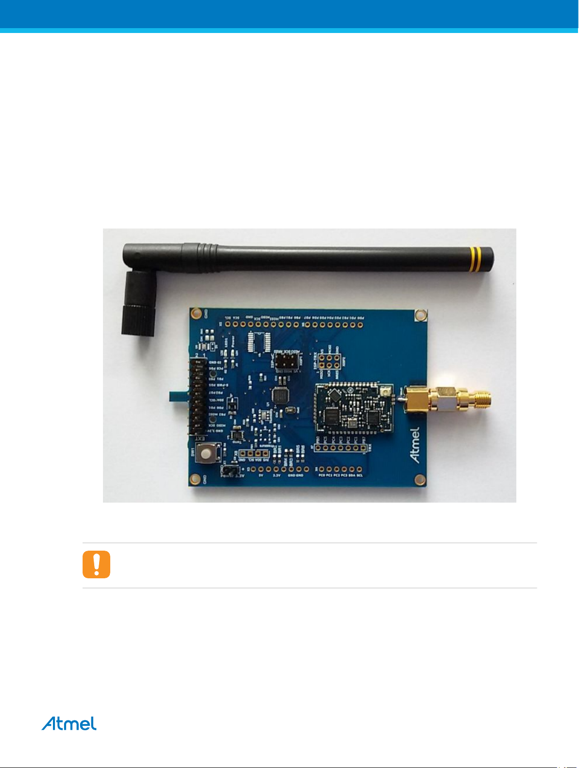
1. Getting Started with the ATA8520-EK1-F Kit
Figure 1-1 shows the components which are included in the evaluation kit. The kit includes
• A single PCB ATAB0102A with
– An Atmel® ATA8520E SIGFOX™ transceiver device
– An Atmel ATmega328P AVR® microcontroller at 8MHz
– An AT30TS75A temperature sensor with TWI
• An 902MHz monopole antenna for connection to the RP-SMA connector
The kit requires an external power supply or battery for 3.0V to 3.3V at 300mA which is not included in
the kit.
Figure 1-1. ATA8520-EK1-F Kit Components
The 902Hz monopole antenna is connected to the RP-SMA connector of the PCB and the external power
supply or battery has to be connected to connector X1.
Caution: Ensure correct polarity at the connection to avoid damage to the equipment. The
PCB has no reverse polarity protection for the power supply connection.
The kit comes with preconfigured devices for starting the Flash application of the Atmel ATmega328P
once the power is applied. This application controls the RF telegram transmission and reads out the
temperature sensor at 15 min. intervals or when pressing the SW1 button. The red LED1 starts blinking
for about 2-3s, i.e. during telegram transmission. The device then enters power-down mode until a wakeup from the internal timer or a button press occurs.
Atmel User Guide for the Evaluation Kit ATA8520-EK1-F and the ATA8520-EK3-F Extension Board (US
Version) [APPLICATION NOTE]
Atmel-9412B-ATAN0156_Application Note-06/2016
5
Page 6

Every fifth transmission is executed as an uplink/downlink request, i.e. it will first transmit the RF telegram
with sensor data and requests a payload data packet from the SIGFOX cloud via a base station. The
execution of these request will take about 40-50s.
The Atmel ATA8520E device includes the SIGFOX ID and PAC registration code (see label attached to
PCB) to register the kit with the user's account for the SIGFOX back end. The user has to open a
SIGFOX cloud account to access the back end. From this account the data payload transmitted from the
devices can be retrieved in various ways as described in the SIGFOX online help.
An Atmel debugger (Atmel JTAGICE3 or Atmel ICE), which can be connected to connector XISP1, is
required for application development. Please see the marker for pin1 to connect with the correct
orientation. The debugger can only be used if Atmel Studio 6 or 7 is installed in the front end. Atmel
Studio 6 or 7 can be downloaded from http://www.atmel.com with additional user instructions and tools.
The documentation for the kit components and for the software is included in the tool pack zip folder [7]
which can be downloaded from the Atmel website [5].
The kit and the boards are preprogrammed and temperature calibrated to operate at room temperature
(24°C). For operation with a wider temperature range a temperature calibration as described in
“ATAN0142 - ATA8520E Crystal Calibration” has to be applied.
Atmel User Guide for the Evaluation Kit ATA8520-EK1-F and the ATA8520-EK3-F Extension Board (US
Version) [APPLICATION NOTE]
Atmel-9412B-ATAN0156_Application Note-06/2016
6
Page 7
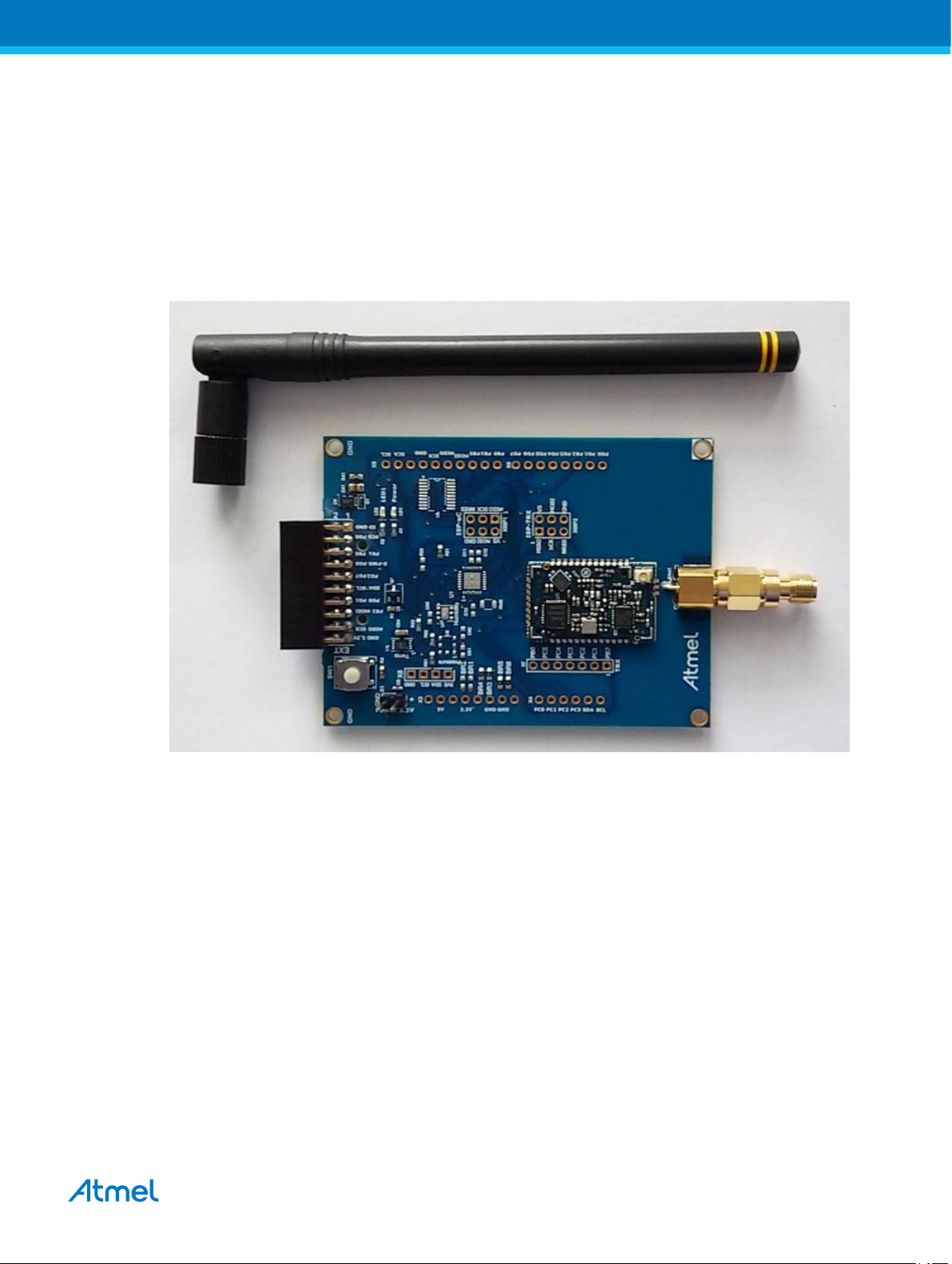
2. Getting Started with the ATA8520-EK3-F Extension Board
The kit as shown in Figure 2-1 includes
• A single PCB ATAB0102A with
– An Atmel® ATA8520E SIGFOX™ transceiver device
– An AT30TS75A temperature sensor with TWI
• An 902MHz monopole antenna for connection to the RP-SMA connector
Figure 2-1. ATA8520-EK3-F Xplained Pro Extension Board
The kit requires an additional XplainedPro SAMD20 or SAMD21 development kit and a 3.0V power
supply with 300mA (connected to X1) as shown in Figure 2-2.
Atmel User Guide for the Evaluation Kit ATA8520-EK1-F and the ATA8520-EK3-F Extension Board (US
Version) [APPLICATION NOTE]
Atmel-9412B-ATAN0156_Application Note-06/2016
7
Page 8
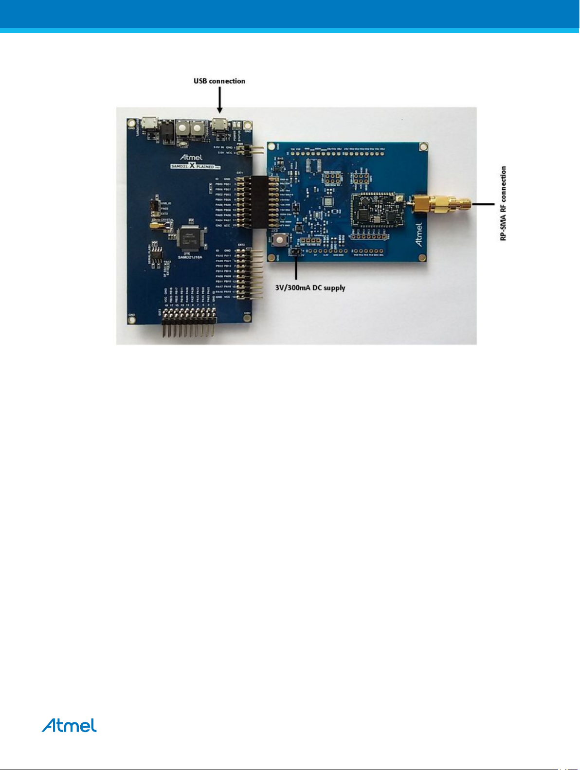
Figure 2-2. ATA8520-EK3-F Xplained Pro Extension Board with SAMD20 or SAMD21 Xplained Pro Kit
The 902MHz monopole antenna is connected to the RP-SMA connector of the PCB and the board is
powered by an external 3V supply.
The tool pack [7] includes an example application for the SAMD20 and SAMD21 Xplained Pro kit at 3V/
48MHz.
This application controls the RF telegram transmission and reads out the temperature sensor at 15minute intervals or when pressing the SW1 button. The red LED1 starts blinking for about 2-3s, i.e. during
telegram transmission. The device then runs in a main loop until an event from the internal timer or a
button press occurs.
Every fifth transmission is executed as an uplink/downlink request, i.e. it will first transmit the RF telegram
with sensor data and requests a payload data packet from the SIGFOX cloud via a base station. The
execution of these request will take about 40-50s.
The ATA8520E device includes the SIGFOX ID and PAC registration code (see label attached on the
PCB) to register the kit with the user's SIGFOX back-end account. The user has to open a SIGFOX cloud
account to access the back end. From this account the data payload transmitted from the devices can be
retrieved in various ways as described in the SIGFOX online help.
The Atmel debugger included in the development kits can be used for application development.
Application development and use of the debugger is only possible if Atmel Studio 6 or 7 is installed in the
front end. Atmel Studio 6 or 7 can be downloaded from http://www.atmel.com with additional user
instructions and tools. The documentation for the kit components and for the software is included in the
tool pack zip folder [7] which can be downloaded from http://www.atmel.com/devices/ATA8520E.aspx.
Atmel User Guide for the Evaluation Kit ATA8520-EK1-F and the ATA8520-EK3-F Extension Board (US
Version) [APPLICATION NOTE]
Atmel-9412B-ATAN0156_Application Note-06/2016
8
Page 9

3. Tool Pack for the Kits
The tool pack zip folder [7] contains the documentation and software for the kit. Extract the folder into a
directory on the PC to get the following structure:
..\Application_Notes documentation for the kit and the application notes for the devices
..\Documentation data sheets of the devices
..\Hardware hardware documentation of the boards
..\Software software for the kit
..\Software\ATA8520-EK1-F Atmel® Studio 6 project directory for ATA8520-EK1-F kit with
..\Software\ATA8520-EK3-F Atmel Studio 6 project directory for ATA8520-EK3-F board with
ATmega328P
SAMD20 or SAMD21 XplainedPro kit
Atmel User Guide for the Evaluation Kit ATA8520-EK1-F and the ATA8520-EK3-F Extension Board (US
Version) [APPLICATION NOTE]
Atmel-9412B-ATAN0156_Application Note-06/2016
9
Page 10

4. ATA8520E SIGFOX Certified Transceiver
The Atmel®ATA8520E SIGFOX™ transceiver includes the SIGFOX protocol library and a SPI
communication interface for controlling device operation. The transceiver buffer of the device is loaded
with a max. of 12 bytes of payload data for transmission in the 902MHz ISM band in the US. The Atmel
ATA8520E device can also receive payload data with 8 Bytes from the SIGFOX cloud when transmitting
an uplink/downlink request. The Atmel ATA8520E device is certified by SIGFOX to participate in their
network. A second certification step for the module or system including antenna is also required with a
classification of the module or system RF performance, i.e. radiated RF output power. As a result, the RF
path including antenna must also have SIGFOX certification.
The key parameters for the RF link of the kits are:
• RF channels: 902MHz to 906MHz for up- and downlink
• RF output power: max. 23dBm
• RF sensitivity: −126dBm
• Data rate: 600bit/s with DBPSK modulation for uplink and 600bit/s with GFSK modulation for
downlink
• Data payload: max. 12byte with LSB first for uplink and 8bytes for downlink
• Data transfer: max. 140 telegrams/day for uplink and max. 4 telegrams/day for downlink
The data transmission is AES encrypted.
The SIGFOX ID and PAC registration code are printed on a label attached to the PCB and can also be
read out from the device using the SPI command interface. This ID and code are required for registering
the device with the user's account for the SIGFOX back end.
Atmel User Guide for the Evaluation Kit ATA8520-EK1-F and the ATA8520-EK3-F Extension Board (US
Version) [APPLICATION NOTE]
Atmel-9412B-ATAN0156_Application Note-06/2016
10
Page 11

5. ATAB0102A PCB Description
Figure 5-1 shows the ATAB0102A PCB used as a platform for the SIGFOX™ kits. It works in two different
modes depending on the component mounted on the PCB:
1. Battery powered standalone operating mode for the ATA8520-EK1-F kit:
– Includes the Atmel® ATA8520E SIGFOX device mounted on a stamp board together with a
Front-End-Module device
– Includes the Atmel ATmega328P AVR® microcontroller with 8MHz internal clock and external
32.768kHz crystal
– Includes the AT30TS75A temperature sensor with TWI
– Includes an RP-SMA antenna connector for an 902MHz external monopole antenna
– Two LEDs:
• Green LED LD1 to indicate the sensor power
• Red LED LD2 connected to port pin PD5 and connector X2/pin8 and X6/pin6 for the
user application
– User button SW1 connected to port pin PD6 and to connectors X2/pin4 and X6/pin7
– Supply voltage divider connected to pin ADC0 to measure the battery voltage against the
internal 1.1V reference
– Includes the footprint for the following TWI sensor devices:
• BMP180 air pressure sensor
• HTU20D/SHT20 humidity sensor
2. Operating mode with an additional Xplained Pro kit for the ATA8520-EK3-F extension board using a
SAMD20 or SAMD21:
– Includes the Atmel ATA8520E SIGFOX device mounted on a stamp board together with a
Front-End-Module device
– Includes the AT30TS75A temperature sensor with TWI
– Includes an RP-SMA antenna connector for an 902MHz external monopole antenna
– Two LEDs:
• Green LED LD1 to indicate the sensor power
• Red LED LD2 connected to port pin PD5 and connector X2/pin8 and X6/pin6 for the
user application
– User button SW1 connected to port pin PD6 and to connectors X2/pin4 and X6/pin7
– Supply voltage divider connected to pin ADC0 to measure the supply voltage against the
internal 1.1V reference
– Includes the footprint for the following TWI sensor devices:
• BMP180 air pressure sensor
• HTU20D / SHT20 humidity sensor
– Includes the connector X2 to for connecting the PCB to an Xplained Pro board
Atmel User Guide for the Evaluation Kit ATA8520-EK1-F and the ATA8520-EK3-F Extension Board (US
Version) [APPLICATION NOTE]
Atmel-9412B-ATAN0156_Application Note-06/2016
11
Page 12

Figure 5-1. ATAB0102A Board
Atmel User Guide for the Evaluation Kit ATA8520-EK1-F and the ATA8520-EK3-F Extension Board (US
Version) [APPLICATION NOTE]
Atmel-9412B-ATAN0156_Application Note-06/2016
12
Page 13

5.1. ATA8520-EK1-F Power Consumption and Battery Selection
10
200.000
i [mA]
TX mode
Measure mode
Power-down mode
8.000
4.500
0.001
2 3 4 5 6 7 8 9 t [s]
When using the PCB in standalone mode, the AVR® microcontroller can be set to a power-down mode
while running the Timer2 with the external 32.768kHz crystal. This will reduce the mean current
consumption to ~10µA to 20µA (see Table 5-1 for 5 messages per day). In this mode the sensor power is
switched off and the Atmel® ATA8520E device is in OFF mode and the MCU only wakes up by pressing
the button, applying an external interrupt signal or from the internal Timer2 interrupt.
Figure 5-2 shows the typical current consumption profile from the different operating modes of the Flash
application during a telegram transmission. This allows the calculation of a mean current consumption
depending on the wake-up intervals.
The shown current profile is a typical profile and depends on the Flash application of the Atmel
ATmega328P device and the attached sensors.
During the telegram transmission the MCU is performing the LED flashing to indicate activity. This
increases the current consumption and can be replaced by setting the MCU in power-down mode. When
the transmission is finished an event is generated on pin PB6 of the ATA8520E which can be used to
wake-up the MCU.
Figure 5-2. Standalone Mode Current Consumption at 24°C
Table 5-1 summarizes battery service life for a typical Lithium battery which can be used with the
ATAB0102A. When selecting the battery, it is important to know the peak current consumption which has
to be supplied by the battery cells. It is assumed that the battery voltage drops from the initial value of 3V
down to 2V at the end of its service life. The self-discharge is defined by the manufacturer as typically 1%
per year at an ambient temperature of 20°C. Battery Life at 20°C
Table 5-1. Battery Life at 20°C
Battery Lifetime (Days and Years)
Messages/Day Mean Current [mA]
(1)
3V Lithium Battery (1800mAh)
Days Years
140 0.383 196 0.5
100 0.274 274 0.7
50 0.138 545 1.5
Atmel User Guide for the Evaluation Kit ATA8520-EK1-F and the ATA8520-EK3-F Extension Board (US
Version) [APPLICATION NOTE]
Atmel-9412B-ATAN0156_Application Note-06/2016
13
Page 14

Messages/Day Mean Current [mA]
20 0.056 1348 3.7
5 0.015 5117 14.0
Note:
1. The mean current values shown in the table are only for indication and cannot be taken as
reference.
When operating in uplink/downlink mode the transmission and reception will take about 40s to 50s. In this
period the device will first send a data telegram three times as shown in Figure 5-2, followed by an idle
mode with about 4.5mA current consumption for about 20s and will then enter the receive mode for about
20s with 19mA current consumption. Finally a confirm telegram is sent for about 0.35s. This uplink/
downlink mode is only possible for max. 4 transmissions/day and has to be added to the Mean Current
consumptions in Table 5-1.
During the uplink/downlink operation the MCU can be placed in power-down mode and can wake-up by
the event of the ATA8520E.
5.2. Connector Description
The PCB has several connectors which are used differently depending on the PCB configuration. Table
5-2 summarizes the connectors and how different PCB versions are used. The placement of the
connectors at the PCB is shown in Figure 5-1.
(1)
Battery Lifetime (Days and Years)
3V Lithium Battery (1800mAh)
Days Years
Table 5-2. ATAB0102A Connectors
Connector ATA8520-EK1-F
Standalone Version
ATA8520-EK3-F
Xplained Pro Extension
X1 ext. power External 3V power supply --
X2 Xplained Pro -- Extension connector
(1)
X3
X4
X5
X6
(1)
(1)
(1)
-- --
-- --
-- --
-- --
X7 RF debug -- --
X8 sensor External sensors External sensors
XISP1 ISP-microcontroller connector --
XISP2 -- --
Note:
1. These connectors can be used to attach a Xplained mini or Arduino UNO kit.
Atmel User Guide for the Evaluation Kit ATA8520-EK1-F and the ATA8520-EK3-F Extension Board (US
Version) [APPLICATION NOTE]
Atmel-9412B-ATAN0156_Application Note-06/2016
14
Page 15

5.2.1. Connector X1
Connector X1 is used for supplying an external 3V power source for standalone battery powered
applications for the ATA8520-EK1-F kit.
Caution: These pins have no reverse polarity protection.
Table 5-3. Connector X1
Function Pin Pin Function
+3.3V 1 2 GND
5.2.2. Connector X2
Connector X2 is used for connecting to an Xplained Pro MCU kit. In this connection mode the PCB is
supplied with 3V of power from the Xplained Pro MCU board.
Table 5-4. Connector X2
Function Pin Pin Function
PC0 (PB00) 3 4 SW1 (PB01)
ID_data 1 2 GND
PB1/RF_NRES (PB06) 5 6 PB0/RF_PWRON (PB07)
SNS_PWR (PB02) 7 8 LED1 (PB03)
RF_EVNT (PB04) 9 10 PD7 (PB05)
SDA (PA08) 11 12 SCL (PA09)
PD0 (PB09) 13 14 PD1 (PB08)
RF_NSS (PA05) 15 16 MOSI (PA06)
MISO (PA04) 17 18 SCK (PA07)
GND 19 20 +3.3V
Note:
Port pins in brackets are for the SAMD20 and SAMD21 device.
5.2.3. Connectors X3, X4, X5 and X6
Connectors X3, X4, X5 and X6 are used for connecting to an Xplained mini or Arduino UNO kit. In this
connection mode the PCB is supplied with 3V and 5V of power from the Xplained mini or Arduino UNO
board.
Connector X3 is used for supplying power to the add-on boards.
Table 5-5. Connector X3
Function Pin
- 1
- 2
Atmel User Guide for the Evaluation Kit ATA8520-EK1-F and the ATA8520-EK3-F Extension Board (US
Version) [APPLICATION NOTE]
Atmel-9412B-ATAN0156_Application Note-06/2016
15
Page 16

Function Pin
- 3
+3.3V 4
+5V 5
GND 6
GND 7
- 8
Connector X4 is used for the port C pins of the MCU.
Table 5-6. Connector X4
Function Pin
PC0 1
PC1 2
PC2 3
PC3 4
PC4/SDA 5
PC5/SCL 6
Connector X5 is used for the port B pins of the MCU. Pins 1 to 6 are connected to a 3V/5V level shifter to
convert the signals to 3V at PCB level.
Table 5-7. Connector X5
Function Pin
PB0/RF_PWRON 1
PB1/RF_NRES 2
PB2/RF_NSS 3
PB3/MOSI 4
PB4/MISO 5
PB5/SCK/LED 6
GND 7
- 8
- 9
- 10
Connector X6 is used for the port D pins of the MCU. Pins 3 and 8 are connected to a 3V/5V level shifter
to convert the signals to 3V at PCB level.
Atmel User Guide for the Evaluation Kit ATA8520-EK1-F and the ATA8520-EK3-F Extension Board (US
Version) [APPLICATION NOTE]
Atmel-9412B-ATAN0156_Application Note-06/2016
16
Page 17

Table 5-8. Connector X6
5.2.4. Connector X7
Connector X7 is not typically mounted. These Atmel® ATA8520E pins can also be used as supplementary
I/O pins.
Table 5-9. Connector X7
Function Pin
PD0 1
PD1 2
PD2/RF_EVNT 3
PD3/SNS_PWR 4
PD4 5
PD5/LED1 6
PD6/SW1 7
PD7 8
Function Pin
5.2.5. Connector X8
Connector X8 is not typically mounted and is used for the TWI bus connection with the switched power
supply. This connector can be used to attach additional sensors and devices with the TWI connection.
The power consumption is limited to ~50mA.
Table 5-10. Connector X8
RPC1/RF_NPRON1 1
RPC2/RF_TRPA 2
RPC3/RF_TMDO 3
RPC4/RF_TMDI 4
RPC5/RF_TRPB 5
RPB7/RF_RX_ACTIVE 6
Function Pin
+3.3Vsens 1
SDA 2
SCL 3
GND 4
5.2.6. Connector ISP-TRX
Connector ISP-TRX is not mounted and is not required for applications.
Atmel User Guide for the Evaluation Kit ATA8520-EK1-F and the ATA8520-EK3-F Extension Board (US
17
Version) [APPLICATION NOTE]
Atmel-9412B-ATAN0156_Application Note-06/2016
Page 18

Table 5-11. Connector ISP-TRX
Function Pin Pin Function
MISO 1 2 VCC
SCK 3 4 MOSI
nRES 5 6 GND
5.2.7. Connector ISP-microcontroller
Connector ISP-microcontroller is used for ATmega328P programming and debugging for the kit ATA8520EK1-F.
Table 5-12. Connector ISP-microcontroller
Function Pin Pin Function
MISO 1 2 V
SCK 3 4 MOSI
nRES 5 6 GND
5.3. LED, Button and Sensors
The green LED LD1 is connected to the sensor power and indicates if the sensor power is switched on.
The red LED LD2 is connected to port PD5 on Atmel® ATmega328P and to the connectors X2/pin8 and
X6/pin6 and can be controlled by the MCU application.
The button SW1 is connected to port PD6 on Atmel ATmega328P and to the connectors X2/pin4 and X6/
pin7 and can be read by the MCU application.
The PCB contains a temperature sensor connected to the TWI bus of the MCU and in addition two
footprints for additional sensors, i.e. an air pressure sensor and a humidity sensor device. With the TWI
connector X8 additional sensors can be connected as long as the current on the 3.3V supply will not
exceed 50mA.
CC
Atmel User Guide for the Evaluation Kit ATA8520-EK1-F and the ATA8520-EK3-F Extension Board (US
Version) [APPLICATION NOTE]
Atmel-9412B-ATAN0156_Application Note-06/2016
18
Page 19

6. Application Description
The Flash application for both kits is set up in the same way with the exceptions described in Table 6-1.
The main differences are found in the CPU and system and Timer2 clock and sleep modes.
Table 6-1. Flash Application Differences
Feature ATA8520-EK1-F ATA8520-EK3-F
Oscillator and CPU clock Internal 8MHz RC oscillator External 32.768kHz crystal
Timer2 External 32.768kHz crystal Internal system clock 48MHz
Sleep mode Power down mode Idle in main loop
System clock 8MHz 48MHz
The source code for all applications is available within the tool pack distribution [7].
The program flow for the Flash application is illustrated in Figure 6-1 and Figure 6-2. The application first
initializes all required peripherals such as pins, timers, SPI, ADC, UART, TWI and the Atmel® ATA8520E
SIGFOX transceiver by reading out the ID/PAC information required for SIGFOX™ registration. This
ID/PAC data is send via the UART interface to a PC terminal application. The Timer2 is used as a realtime clock and uses either the
• External 32.768kHz crystal for the ATA8520-EK1-F kit or the
• Internal system clock for the ATA8520-EK3-F kit.
Xplained Pro
Timer2 is configured to wake up the MCU every 15 minutes. Pressing button SW1 also causes the MCU
to wake up. The temperature sensor is powered up and read out and after this a data telegram is
transmitted. The device then enters power-down mode again until the next wake-up by the RTC (or
manually by pressing SW1).
Atmel User Guide for the Evaluation Kit ATA8520-EK1-F and the ATA8520-EK3-F Extension Board (US
Version) [APPLICATION NOTE]
Atmel-9412B-ATAN0156_Application Note-06/2016
19
Page 20

Figure 6-1. Flash Application Flow Chart 1
Start
yes
yes
yes
no
no
Initialization 1
Init pins, Timer0, Timer2, SPI,
ADC
20s timer
expired?
Initialization 2
Init UART, TWI, ATA8520E
and read and print ID/PAC
Switch to power-own mode
(ATA8520-EK1-F only)
Switch sensor power
RF transmitter and LED on
Reset channel usage
Transmit as Downlink
Frame and receive data
payload
Transmit as Uplink Frame
Switch sensor power off
Read out temperature sensor
and convert result
Switch RF transmitter
and LED off
Check and wait if button
released
Transmit
count ≥ 4?
Timer2 event
or button pressed?
no
yes
yes
Transmit as Downlink
Frame and receive data
payload
Blink LED
Read RX buffer data
Done
Done
Transmit as Uplink Frame
Load data in TX buffer
and transmit
Load data in TX buffer
and transmit
Is transmit
finished?
Blink LED
no
Is transmit
finished?
Figure 6-2. Flash Application Flow Chart 2
During the step Initialization1 the application will perform a check for the device version to be V2.3. This
device version supports the US mode operation.
Atmel User Guide for the Evaluation Kit ATA8520-EK1-F and the ATA8520-EK3-F Extension Board (US
Version) [APPLICATION NOTE]
Atmel-9412B-ATAN0156_Application Note-06/2016
20
Page 21

6.1. Software Development
Atmel® Studio 6 or 7 is required for software development and can be downloaded from the Atmel
website [5]. The tool pack [7] with software and documentation is also required. When unpacking the tool
pack, the folder structure as described in Tool Pack for the Kits is generated.
Three different applications and folder structures are included with sample applications for the kit
versions.
..\ATA8520-EK1-F\ATAB0102A ATmega328P project for ATA8520-EK1-F kit
..\ATA8520-EK3-F\SAMD20_XplainedPRO_SW SAMD20 Xplained Pro project for ATA8520-EK3 kit
..\ATA8520-EK3-F\SAMD21_XplainedPRO_SW SAMD21 Xplained Pro project for ATA8520-EK3 kit
-----------------------------------------------------
The Atmel Studio 6 or 7 installation makes all USB drivers and debugger supports available when
plugging in the development kits. The ATA8520-EK1-F standalone kit may require an AVR® debugger
connected to the connector ISP-microcontroller for debugging and programming, which is not included in
the kit.
6.2. FCC Compliance Application
To be compliant with the FCC regulations according the RF transmission the following SPI commands
and sequences have to be used in the application code.
During End-Of-Line testing of the hardware and the ATA8520E device the following settings have to be
applied and configured in the EEPROM as described in the data sheet of the ATA8520E device:
• The RF transmit frequency has to be set to 902.2MHz
• The RF receive frequency has to be set to 905.2MHz
• The US mode has to be enabled in the EEPROM configuration
• The channel usage has to be configured with 9 macro channels
• Each macro channel will use 6 micro channels
The SPI commands for the configuration are summarized in Table 6-2.
Table 6-2. SPI Commands and Parameters for ATA8520E Configuration
SPI Command Parameter Description
Store System Configuration
(0x11)
DDRC, PORTC, 0x02, 0x3B Enable US mode with up-/
downlink and 3V supply
Store Frequencies (0x1A) 902200000, 905200000 Store TX and RX frequencies
[Hz]
Store Channel Configuration
(0x22)
0xFF, 0x01, 0x00, 0x00,
0x00, 0x00, 0x00, 0x00,
Enable 9 macro channels from
902.2 to 904.6MHz
0x00, 0x00, 0x00, 0x00,
0x01, 0x00
The application flow has to be according to Figure 6-3 for the transmission of message payload up to 12
byte using the described SPI commands.
Atmel User Guide for the Evaluation Kit ATA8520-EK1-F and the ATA8520-EK3-F Extension Board (US
Version) [APPLICATION NOTE]
Atmel-9412B-ATAN0156_Application Note-06/2016
21
Page 22

Figure 6-3. Application Flow
Power-up
Reset channel usage (0x23)
yes
yes
no
no
Initialization
Wake-up and init ATA8520E
Read status
(0x0A)
20s timer
expired?
Read RX data buffer (0x10)
(only when performing
downlink operation)
Read status (0x0A)
Load up to 12 byte in
TX buffer (0x07)
Wake-up and init ATA8520E
Read status (0x0A)
Switch into OFF Mode
(0x05)
Transmit data
(0x0D or 0x0E)
Event
received?
The SPI commands for the application flow are summarized in Table 6-3.
Table 6-3. SPI Commands and Parameters for ATA8520E Application
SPI Command Parameter Description
Get Status (0x0A) Status information returned Read ATA8520E device status
and clear a pending event
Reset channel usage (0x23) none Reset channel usage scheme for
macro and micro channels
Write TX buffer (0x07) Up to 12 byte payload data Load transmit buffer with payload
data
Send Frame (0x0D) None Transmit data frame and
Send/Receive Frame (0x0E) None Transmit data frame, wait for
generate event when finished
receive frame and generate
event when finished
Read RX buffer (0x10) 8 byte returned Read receive buffer data
OFF mode (0x05) None Switch ATA8520E into OFF mode
(Wake-up is performed with
PWRON or NPWRONx pins)
To be compliant with the FCC transmission requirements a 20 seconds idle time has to be performed
after wake-up of the ATA8520E device.
Atmel User Guide for the Evaluation Kit ATA8520-EK1-F and the ATA8520-EK3-F Extension Board (US
Version) [APPLICATION NOTE]
Atmel-9412B-ATAN0156_Application Note-06/2016
22
Page 23

7. Revision History
Please note that the following page numbers referred to in this section refer to the specific revision
mentioned, not to this document.
Revision No. History
9412B-06/16
• Figure 1-1 "ATA8520-EK1-F Kit Components" on page 5
updated
• Figure 2-1 "ATA8520-EK3-F Xplained Pro Extension Board" on
page 7 updated
• Figure 2-2 "ATA8520-EK3-F Xplained Pro Extension Board
with SAMD20 or SAMD21 Xplained Pro Kit" on page 8
updated
Atmel User Guide for the Evaluation Kit ATA8520-EK1-F and the ATA8520-EK3-F Extension Board (US
Version) [APPLICATION NOTE]
Atmel-9412B-ATAN0156_Application Note-06/2016
23
Page 24

Atmel Corporation 1600 Technology Drive, San Jose, CA 95110 USA T: (+1)(408) 441.0311 F: (+1)(408) 436.4200 | www.atmel.com
©
2016 Atmel Corporation. / Rev.: Atmel-9412B-ATAN0156_Application Note-06/2016
Atmel®, Atmel logo and combinations thereof, Enabling Unlimited Possibilities®, and others are registered trademarks or trademarks of Atmel Corporation in U.S. and
other countries. Other terms and product names may be trademarks of others.
DISCLAIMER: The information in this document is provided in connection with Atmel products. No license, express or implied, by estoppel or otherwise, to any
intellectual property right is granted by this document or in connection with the sale of Atmel products. EXCEPT AS SET FORTH IN THE ATMEL TERMS AND
CONDITIONS OF SALES LOCATED ON THE ATMEL WEBSITE, ATMEL ASSUMES NO LIABILITY WHATSOEVER AND DISCLAIMS ANY EXPRESS, IMPLIED
OR STATUTORY WARRANTY RELATING TO ITS PRODUCTS INCLUDING, BUT NOT LIMITED TO, THE IMPLIED WARRANTY OF MERCHANTABILITY,
FITNESS FOR A PARTICULAR PURPOSE, OR NON-INFRINGEMENT. IN NO EVENT SHALL ATMEL BE LIABLE FOR ANY DIRECT, INDIRECT,
CONSEQUENTIAL, PUNITIVE, SPECIAL OR INCIDENTAL DAMAGES (INCLUDING, WITHOUT LIMITATION, DAMAGES FOR LOSS AND PROFITS, BUSINESS
INTERRUPTION, OR LOSS OF INFORMATION) ARISING OUT OF THE USE OR INABILITY TO USE THIS DOCUMENT, EVEN IF ATMEL HAS BEEN ADVISED
OF THE POSSIBILITY OF SUCH DAMAGES. Atmel makes no representations or warranties with respect to the accuracy or completeness of the contents of this
document and reserves the right to make changes to specifications and products descriptions at any time without notice. Atmel does not make any commitment to
update the information contained herein. Unless specifically provided otherwise, Atmel products are not suitable for, and shall not be used in, automotive
applications. Atmel products are not intended, authorized, or warranted for use as components in applications intended to support or sustain life.
SAFETY-CRITICAL, MILITARY, AND AUTOMOTIVE APPLICATIONS DISCLAIMER: Atmel products are not designed for and will not be used in connection with any
applications where the failure of such products would reasonably be expected to result in significant personal injury or death (“Safety-Critical Applications”) without
an Atmel officer's specific written consent. Safety-Critical Applications include, without limitation, life support devices and systems, equipment or systems for the
operation of nuclear facilities and weapons systems. Atmel products are not designed nor intended for use in military or aerospace applications or environments
unless specifically designated by Atmel as military-grade. Atmel products are not designed nor intended for use in automotive applications unless specifically
designated by Atmel as automotive-grade.
Page 25

Mouser Electronics
Authorized Distributor
Click to View Pricing, Inventory, Delivery & Lifecycle Information:
Atmel:
ATA8520-EK3-F
 Loading...