

Page 1

APPLICATION NOTE
User Guide for the Evaluation Kit A TA8520-EK1-E and the
ATA8520-EK2-E and ATA8520-EK3-E Extension Boards
ATAN0104
Features
● User guide for the evaluation kit ATA8520-EK1-E and extension boards
ATA8520-EK2-E and ATA8520-EK3-E
● This kit demonstrates a Flash application with the
● ATA8520-EK1-E evaluation kit:
with the Atmel
ATmega328P AVR
battery-powered kit for standalone operation
● ATA8520-EK2-E and
Includes Atmel SIGFOX ATA8520D V1.3 transceiver device with an AT30TS75A
temperature monitoring device. An additional MCU application development kit,
i.e. Xplained mini or Arduino UNO is required.
®
SIGFOX™ ATA8520D V1.3 transceiver device and an Atmel
®
microcontroller with AT30TS75A temperature sensor as a
ATA8520-EK3-E extension boards:
Description
This user guide describes an evaluation kit and the extension boards for a SIGFOX
application. This application uses an Atmel ATmega328P AVR microcontroller to
read out an AT30TS75A temperature sensor using the built-in TWI connection and controls
the RF telegram transmission using the SIGFOX ATA8520D V1.3 transceiver device. This
application requires a SIGFOX base station infrastructure to capture the RF telegram and
supply payload data at the SIGFOX back end of the SIGFOX Cloud. For more information
on operating the SIGFOX network and SIGFOX Cloud, see http://www.sigfox.com
information.
The evaluation and development kit tool packs are available for download from the Atmel
website: http://www.atmel.com/devices/ATA8520.aspx. These tool packs include
● The ATAN0054 quick start guide for the kit and the Atmel ATAN0104 user guide
● The schematic, layout and Gerber data for the ATAB0101A PCB
● The source code for the Atmel ATmega328P as an Atmel Studio 6 project
The Atmel ATA8520D SIGFOX transceiver is a SIGFOX-certified device which includes the
complete SIGFOX protocol stack to operate in the SIGFOX network within the 868MHz
ISM band. The device is controlled from any host MCU using the SPI commands as
described in the datasheet [1]. Included in the tool pack is a ATA8520D library as C source
code for the SPI commands.
9373E-AUTO-11/15
Page 2

References
[1] Atmel® ATA8520D datasheet and user guide
[2] Atmel AT30TS75A datasheet
[3] http://www.sigfox.com
[4] http://backend.sigfox.com
[5] http://www.atmel.com/devices/ATA8520.aspx
[6] Atmel ATAN0054 – ATA8520-EK1-E/EK2-E/EK3-E quick start guide
[7] ATA8520-EK123-E_Tool_pack_V1.0.zip
2
ATAN0104 [APPLICATION NOTE]
9373E–AUTO–11/15
Page 3
1. Getting Started with the ATA8520-EK1-E Kit
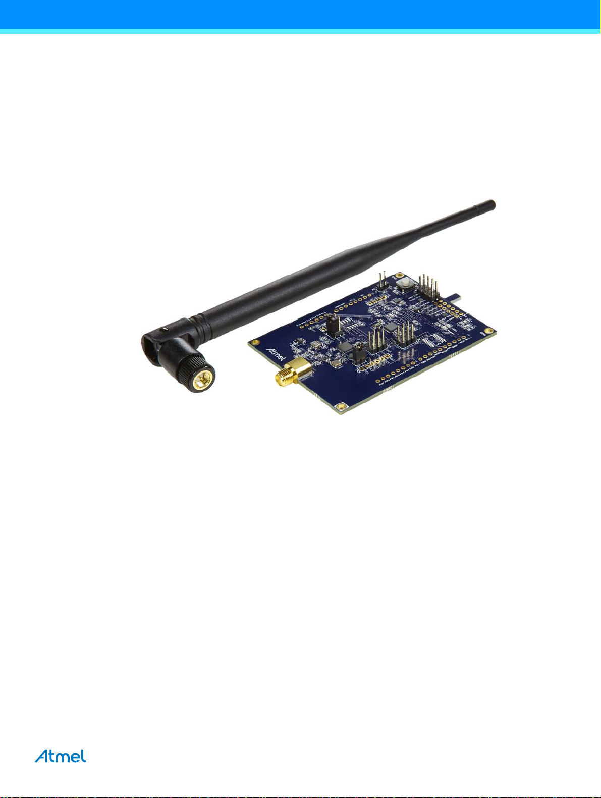
Figure 1-1 shows the components which are included in the evaluation kit. The kit includes
● A single PCB ATAB0101A with
● An Atmel
● An Atmel ATmega328P AVR
● An AT30TS75A temperature sensor with TWI
● An 868MHz monopole antenna for connection to the SMA connector
The kit requires an external power supply or battery for 3.0V to 3.3V at 50mA which is not included in the kit.
Figure 1-1. ATA8520-EK1-E Kit Components
®
ATA8520D SIGFOX™ transceiver device
®
microcontroller at 8MHz
The 868MHz monopole antenna is connected to the SMA connector of the PCB and the external power supply or battery has
to be connected to connector X1.
Caution: Ensure correct polarity at the connection to avoid damage to the equipment. The PCB has no reverse polarity
protection for the power supply connection.
The kit comes with preconfigured devices for starting the Flash application of the Atmel ATmega328P once the power is
applied. This application controls the RF telegram transmission and reads out the temperature sensor at one-hour intervals
or when pressing the SW1 button. The red LED1 starts blinking for about 7-8s, i.e. during telegram transmission. The device
then enters power-down mode until a wake-up from the internal timer or a button press occurs.
Every fifth transmission is executed as an uplink/downlink request, i.e. it will first transmit the RF telegram with sensor data
and requests a payload data packet from the SIGFOX cloud via a base station. The execution of these request will take
about 40-50s.
The Atmel ATA8520D device includes the SIGFOX ID and PAC registration code (see label attached to PCB) to register the
kit with the user's account for the SIGFOX back end. The user has to open a SIGFOX cloud account to access the back end.
From this account the data payload transmitted from the devices can be retrieved in various ways as described in the
SIGFOX online help.
An Atmel debugger (Atmel JTAGICE3 or Atmel ICE), which can be connected to connector XISP1, is required for application
development. Please see the marker for pin1 to connect with the correct orientation. The debugger can only be used if
Atmel Studio 6 is installed in the front end. Atmel Studio 6 can be downloaded from http://www.atmel.com with additional
user instructions and tools. The documentation for the kit components and for the software is included in the tool pack zip
folder [7] which can be downloaded from the Atmel website [5].
The kit and the boards are preprogrammed and temperature calibrated to operate at room temperature (24°C). For operation
with a wider temperature range a temperature calibration as described in “ATAN0142 - ATA8520D Crystal Calibration” has
to be applied. This is mandatory to comply with the CE certification for the kit and boards and is valid for a temperature range
of –20°C to +55°C.
ATAN0104 [APPLICATION NOTE]
9373E–AUTO–11/15
3
Page 4
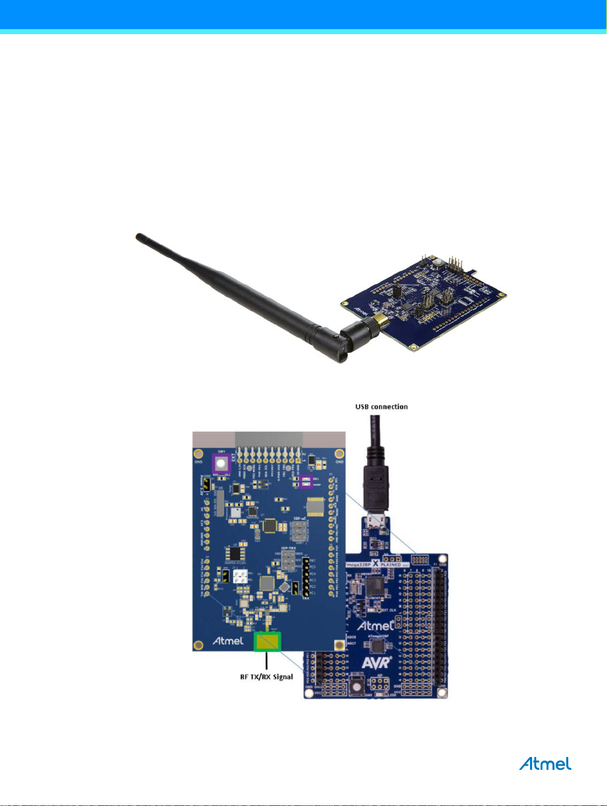
2. Getting Started with the ATA8520-EK2-E and -EK3-E Extension Boards
Figure 2-1 and Figure 2-4 show the components which are required for the evaluation kit. The kit includes
● A single PCB ATAB0101A with
● An Atmel
● An AT30TS75A temperature sensor with TWI
● An 868MHz monopole antenna for connection to the SMA connector
The kit is available in two versions depending on the connector type of the additionally required development kit:
● An ATA8520-EK2-E Xplained mini (Figure 2-1): to be used with an additional Xplained mini (Figure 2-2) or Arduino
UNO kit
● An ATA8520-EK3-E Xplained Pro (Figure 2-3): to be used with an additional Xplained Pro kit (Figure 2-4)
Figure 2-1. ATA8520-EK2-E Xplained Mini Extension Board with Attached External Antenna
®
ATA8520D SIGFOX™ transceiver device
Figure 2-2. ATA8520-EK2-E Xplained Mini Extension Board Mounted on Xplained Mini
4
ATAN0104 [APPLICATION NOTE]
9373E–AUTO–11/15
Page 5
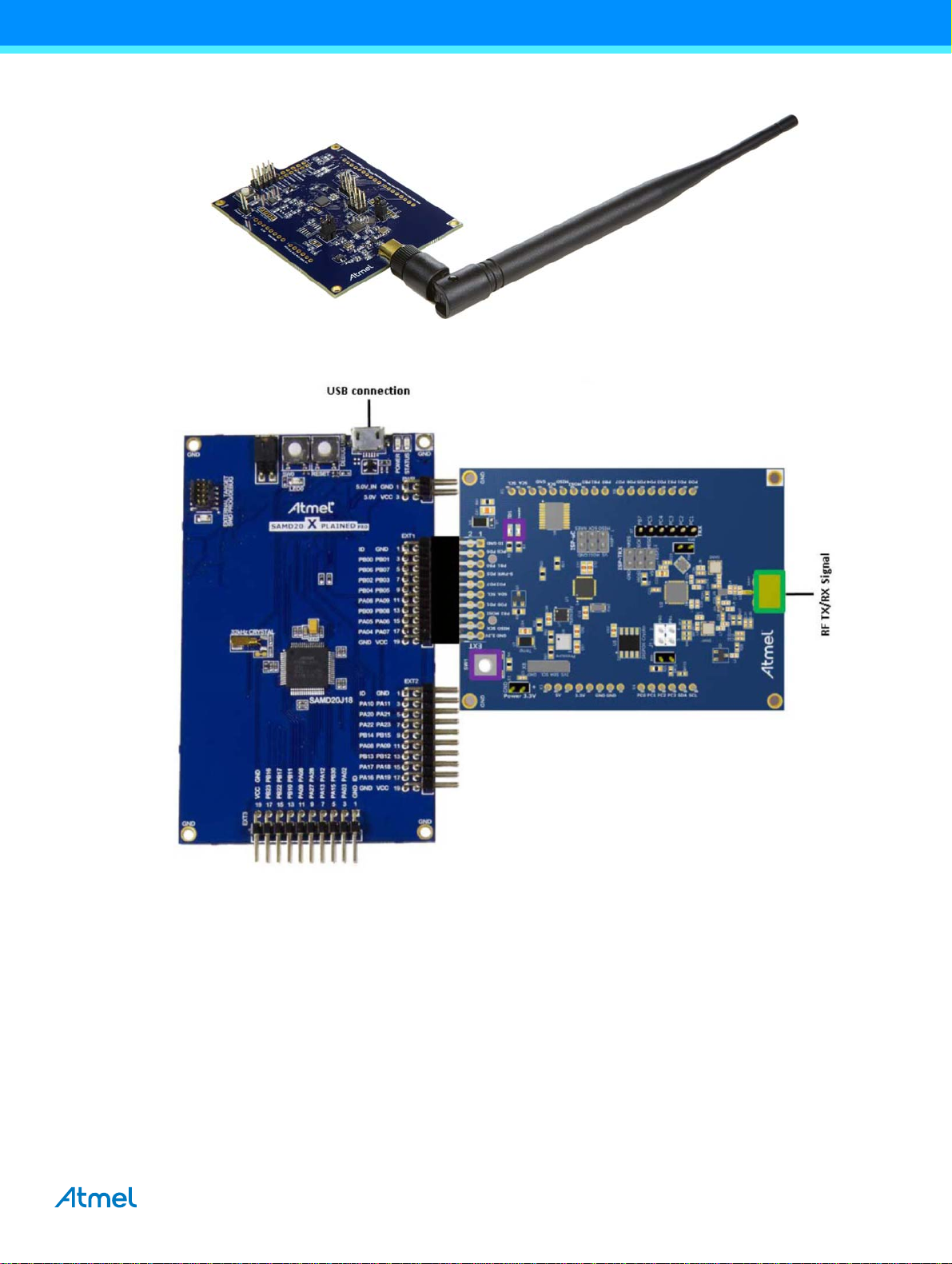
Figure 2-3. ATA8520-EK3-E Xplained Pro Extension Board
Figure 2-4. ATA8520-EK3-E Xplained Pro Extension Board with SAMD21 Xplained Pro Kit
The 868MHz monopole antenna is connected to the SMA connector of the PCB and the board is powered from the attached
evaluation kit using 3V/5V for the ATA8520-EK2-E Xplained Mini and 3V for the ATA8520-EK3-E Xplained Pro.
The following Flash applications are available as part of tool pack distribution:
● Xplained mini – Atmega328P application at 5V/16MHz
● Arduino UNO sketch and library at 5V/16MHz
● SAMD21 application for Xplained Pro at 3V/48MHz
This application controls the RF telegram transmission and reads out the temperature sensor at 15-minute intervals or when
pressing the SW1 button. The red LED1 starts blinking for about 7-8s, i.e. during telegram transmission. The device then
runs in a main loop until an event from the internal timer or a button press occurs.
ATAN0104 [APPLICATION NOTE]
9373E–AUTO–11/15
5
Page 6

Every fifth transmission is executed as an uplink/downlink request, i.e. it will first transmit the RF telegram with sensor data
and requests a payload data packet from the SIGFOX cloud via a base station. The execution of these request will take
about 40-50s.
The ATA8520D device includes the SIGFOX ID and PAC registration code (see label attached on the PCB) to register the kit
with the user's SIGFOX back-end account. The user has to open a SIGFOX cloud account to access the back end. From this
account the data payload transmitted from the devices can be retrieved in various ways as described in the SIGFOX online
help.
The Atmel debugger included in the development kits can be used for application development. Application development
and use of the debugger is only possible if Atmel Studio 6 is installed in the front end. Atmel Studio 6 can be downloaded
from http://www.atmel.com with additional user instructions and tools. The documentation for the kit components and for the
software is included in the tool pack zip folder [7] which can be downloaded from
http://www.atmel.com/devices/ATA8520.aspx.
6
ATAN0104 [APPLICATION NOTE]
9373E–AUTO–11/15
Page 7

3. Tool Pack for the Kits
The tool pack zip folder [7] contains the documentation and software for the kit. Extract the folder into a directory on the PC
to get the following structure:
..\Application_Notes documentation for the kit and the application notes for the devices
..\Documentation data sheets of the devices
..\Hardware hardware documentation of the boards
..\Software software for the kit
..\Software\ATA8520-EK1-E Atmel
..\Software\ATA8520-EK2-E Atmel Studio 6 project directory for ATA8520-EK2-E board with Atmega328P
..\Software\ATA8520-EK3-E Atmel Studio 6 project directory for ATA8520-EK3-E board with SAMD21
®
Studio 6 project directory for ATA8520-EK1-E kit with ATmega328P
4. ATA8520D SIGFOX Certified Transceiver
The Atmel ATA8520D SIGFOX™ transceiver includes the SIGFOX protocol library and a SPI communication interface for
controlling device operation. The transceiver buffer of the device is loaded with a max. of 12 bytes of payload data for
transmission in the 868MHz ISM band. The ATA8520D device can also receive payload data with 8 Bytes from the SIGFOX
cloud when transmitting an uplink/downlink request. The Atmel ATA8520D device is certified by SIGFOX to participate in
their network. A second certification step for the module or system including antenna is also required with a classification of
the module or system RF performance, i.e. radiated RF output power. As a result, the RF path including antenna must also
have SIGFOX certification.
The key parameters for the RF link are:
● RF channels: 868.0 to 868.6MHz for uplink and 869.4 to 869.65MHz for downlink
● RF output power: max. 14.5dBm
● RF sensitivity: –126dBm
● Data rate: 100bit/s with DBPSK modulation for uplink and 600bit/s with GFSK modulation for downlink
● Data payload: max. 12byte with LSB first for uplink and 8 bytes for downlink
● Duty cycle: max. 5 telegrams/hour, i.e. < 1% for uplink and max. 4 telegrams/day for downlink
The data transmission is AES encrypted.
The SIGFOX ID and PAC registration code are printed on a label attached to the PCB and can also be read out from the
device using the SPI command interface. This ID and code are required for registering the device with the user's account for
the SIGFOX back end.
ATAN0104 [APPLICATION NOTE]
9373E–AUTO–11/15
7
Page 8

5. ATAB0101A PCB Description
Figure 5-1 on page 9 shows the ATAB0101A PCB used as a platform for the SIGFOX™ kits. It works in three different modes
depending on the component mounted on the PCB:
1. Battery powered standalone operating mode for the ATA8520-EK1-E kit:
● Includes the Atmel
● Includes the Atmel ATmega328P AVR
crystal
● Includes the AT30TS75A temperature sensor with TWI
● Includes an ATAES132 crypto device (footprint)
● Includes an SMA antenna connector for an 868MHz external monopole antenna
● Two LEDs:
i. Green LED LD1 to indicate the sensor power
ii. Red LED LD2 connected to port pin PD5 and connector X2/pin8 and X6/pin6 for the user application
● User button SW1 connected to port pin PD6 and to connectors X2/pin4 and X6/pin7
● Supply voltage divider connected to pin ADC0 to measure the battery voltage against the internal 1.1V
reference
● Includes the footprint for the following TWI sensor devices:
i. BMP180 air pressure sensor
ii. HTU20D/SHT20 humidity sensor
2. Operating mode with an additional Xplained mini or Arduino UNO kit for the ATA8520-EK2-E extension board
using an ATmega328P:
● Includes the Atmel ATA8520D SIGFOX device
● Includes the AT30TS75A temperature sensor with TWI
● Includes an ATAES132 crypto device (footprint)
● Includes an SMA antenna connector for an 868MHz external monopole antenna
● Two LEDs:
i. Green LED LD1 to indicate the sensor power
ii. Red LED LD2 connected to port pin PD5 and connector X2/pin8 and X6/pin6 for the user application
● User button SW1 connected to port pin PD6 and to connectors X2/pin4 and X6/pin7
● Supply voltage divider connected to pin ADC0 to measure the supply voltage against the internal 1.1V
reference
● Includes the footprint for the following TWI sensor devices:
i. BMP180 air pressure sensor
ii. HTU20D / SHT20 humidity sensor
● Includes the connectors X3, X4, X5 and X6 for connecting the PCB on top of an Xplained mini or an Arduino
UNO board
3. Operating mode with an additional Xplained Pro kit for the ATA8520-EK3-E extension board using a SAMD21:
● Includes the Atmel ATA8520D SIGFOX device
● Includes the AT30TS75A temperature sensor with TWI
● Includes an ATAES132 crypto device (footprint)
● Includes an SMA antenna connector for an 868MHz external monopole antenna
● Two LEDs:
i. Green LED LD1 to indicate the sensor power
ii. Red LED LD2 connected to port pin PD5 and connector X2/pin8 and X6/pin6 for the user application
● User button SW1 connected to port pin PD6 and to connectors X2/pin4 and X6/pin7
®
ATA8520D SIGFOX device
®
microcontroller with 8MHz internal clock and external 32.768kHz
8
ATAN0104 [APPLICATION NOTE]
9373E–AUTO–11/15
Page 9

● Supply voltage divider connected to pin ADC0 to measure the supply voltage against the internal 1.1V
reference
● Includes the footprint for the following TWI sensor devices:
i. BMP180 air pressure sensor
ii. HTU20D / SHT20 humidity sensor
● Includes the connector X2 to for connecting the PCB to an Xplained Pro board
Figure 5-1. ATAB0101A Board
ATAN0104 [APPLICATION NOTE]
9373E–AUTO–11/15
9
Page 10

5.1 ATA8520-EK1-E Power Consumption and Battery Selection
When using the PCB in standalone mode, the AVR® microcontroller can be set to a power-down mode while running the
Timer2 with the external 32.768kHz crystal. This will reduces the mean current consumption to ~10 to 20µA (see Table 5-1
for 5 messages per day). In this mode the sensor power is switched off and the Atmel
and the MCU only wakes up by pressing the button, applying an external interrupt signal or from the internal Timer2
interrupt.
Figure 5-2 shows the typical current consumption profile from the different operating modes of the Flash application during a
telegram transmission. This allows the calculation of a mean current consumption depending on the wake-up intervals.
The shown current profile is a typical profile and depends on the Flash application of the Atmel ATmega328P device and the
attached sensors.
During the telegram transmission the MCU is performing the LED flashing to indicate activity. This increases the current
consumption and can be replaced by setting the MCU in power-down mode. When the transmission is finished an event is
generated on pin PB6 of the ATA8520D which can be used to wake-up the MCU.
Figure 5-2. Standalone Mode Current Consumption at 24°C
®
ATA8520D device is in OFF mode
10
Table 5-1 summarizes battery service life for a typical Lithium battery which can be used with the ATAB0101A. When
selecting the battery, it is important to know the peak current consumption which has to be supplied by the battery cells. It is
assumed that the battery voltage drops from the initial value of 3V down to 2V at the end of its service life. The self-discharge
is defined by the manufacturer as typically 1% per year at an ambient temperature of 20°C.
Table 5-1. Battery Life at 20°C
Battery Lifetime (Days and Years)
3V Lithium Battery (1800mAh)
Messages/Day Mean Current [mA]
(1)
Days Years
140 0.421 178 0.5
100 0.301 249 0.7
50 0.151 497 1.4
20 0.061 1230 3.4
5 0.016 4689 12.8
Note: 1. The mean current values shown in the table are only for indication and cannot be taken as reference.
ATAN0104 [APPLICATION NOTE]
9373E–AUTO–11/15
Page 11

When operating in uplink/downlink mode the transmission and reception will take about 40 to 50 seconds. In this period the
device will first send a data telegram three times as shown in Figure 5-2, followed by an idle mode with about 4.5mA current
consumption for about 20s and will then enter the receive mode for about 20s with 19mA current consumption. Finally a
confirm telegram is sent for about 2s. This uplink/downlink mode is only possible for max. 4 transmissions/day and has to be
added to the Mean Current consumptions in Table 5-1.
During the uplink/downlink operation the MCU can be placed in power-down mode and can wake-up by the event of the
ATA8520D.
5.2 Connector Description
The PCB has several connectors which are used differently depending on the PCB configuration. Table 5-2 summarizes the
connectors and how different PCB versions are used.
The placement of the connectors at the PCB is shown in Figure 5-1 on page 9.
Table 5-2. ATAB0101A Connectors
Connector
X1 ext. power External 3V power supply -- --
X2 Xplained Pro -- Extension connector --
X3 Xplained mini -- -- Shield connector1
X4 Xplained mini -- -- Shield connector2
X5 Xplained mini -- -- Shield connector3
X6 Xplained mini -- -- Shield connector4
X7 RF debug -- -- --
X8 sensor External sensors External sensors External sensors
J1 RF config. PB0/PB1 pin usage PB0/PB1 pin usage PB0/PB1 pin usage
XISP1 ISP-microcontroller connector -- --
XISP2 -- -- --
5.2.1 Connector X1
Connector X1 is used for supplying an external 3V power source for standalone battery powered applications for the
ATA8520-EK1-E kit.
Caution: These pins have no reverse polarity protection.
Table 5-3. Connector X1
ATA8520-EK1-E
Standalone Version
ATA8520-EK3-E
Xplained Pro Extension
ATA8520-EK2-E
Xplained Mini Extension
Function Pin Pin Function
+3.3V 1 2 GND
ATAN0104 [APPLICATION NOTE]
9373E–AUTO–11/15
11
Page 12

5.2.2 Connector X2
Connector X2 is used for connecting to an Xplained Pro MCU kit. In this connection mode the PCB is supplied with 3V of
power from the Xplained Pro MCU board.
Table 5-4. Connector X2
Function Pin Pin Function
ID_data 1 2 GND
PC0 (PB00) 3 4 SW1 (PB01)
PB1/RF_NRES (PB06) 5 6 PB0/RF_PWRON (PB07)
SNS_PWR (PB02) 7 8 LED1 (PB03)
RF_EVNT (PB04) 9 10 AES_NSS (PB05)
SDA (PA08) 11 12 SCL (PA09)
PD0 (PB09) 13 14 PD1 (PB08)
RF_NSS (PA05) 15 16 MOSI (PA06)
MISO (PA04) 17 18 SCK (PA07)
GND 19 20 +3.3V
5.2.3 Connectors X3, X4, X5 and X6
Connectors X3, X4, X5 and X6 are used for connecting to an Xplained mini or Arduino UNO kit. In this connection mode the
PCB is supplied with 3V and 5V of power from the Xplained mini or Arduino UNO board.
Connector X3 is used for supplying power to the add-on boards.
Table 5-5. Connector X3
Function Pin
- 1
- 2
- 3
+3.3V 4
+5V 5
GND 6
GND 7
- 8
Connector X4 is used for the port C pins of the MCU.
Table 5-6. Connector X4
Function Pin
PC0 1
PC1 2
PC2 3
PC3 4
PC4/SDA 5
PC5/SCL 6
12
ATAN0104 [APPLICATION NOTE]
9373E–AUTO–11/15
Page 13

Connector X5 is used for the port B pins of the MCU. Pins 1 to 6 are connected to a 3V/5V level shifter to convert the signals
to 3V at PCB level.
Table 5-7. Connector X5
Function Pin
PB0/RF_PWRON 1
PB1/RF_NRES 2
PB2/RF_NSS 3
PB3/MOSI 4
PB4/MISO 5
PB5/SCK/LED 6
GND 7
- 8
- 9
- 10
Connector X6 is used for the port D pins of the MCU. Pins 3 and 8 are connected to a 3V/5V level shifter to convert the
signals to 3V at PCB level.
Table 5-8. Connector X6
5.2.4 Connector X7
Connector X7 is not typically mounted. These Atmel® ATA8520D pins can also be used as supplementary I/O pins.
Table 5-9. Connector X7
Function Pin
PD0 1
PD1 2
PD2/RF_EVNT 3
PD3/SNS_PWR 4
PD4 5
PD5/LED1 6
PD6/SW1 7
PD7/AES_NSS 8
Function Pin
RPC1/RF_NPRON1 1
RPC2/RF_TRPA 2
RPC3/RF_TMDO 3
RPC4/RF_TMDI 4
RPC5/RF_TRPB 5
RPB7/RF_RX_ACTIVE 6
ATAN0104 [APPLICATION NOTE]
9373E–AUTO–11/15
13
Page 14

5.2.5 Connector X8
Connector X8 is not typically mounted and is used for the TWI bus connection with the switched power supply. This
connector can be used to attach additional sensors and devices with the TWI connection. The power consumption is limited
to ~50mA.
Table 5-10. Connector X8
5.2.6 Connector J1 and BR8
The connector J1 is used for connecting the NPWRON1 and NRES pins of the ATA8520D to the PB0 and PB1 port pins of
the MCU. If the PB0 and PB1 pins are used for other purposes, these connections are removed. In this case the PWRON pin
can be connected to pin NSS of the ATA8520D using the jumper BR8. A device reset can also be forced using the “system
reset” SPI command.
Per default the following connections are set: jumper on J1 between pin3 and 4 for the NRES signal and a connection
between J1/pin2 to BR8/pin2 for the PWRON signal (the NPWRON1 signal is not used for wake-up of the device).
Table 5-11. Connector J1
Function Pin
+3.3Vsens 1
SDA 2
SCL 3
GND 4
Function Pin Pin Function
RF_PWRON1 1 2 PB0
RF_NRES 3 4 PB1
Table 5-12. Connector BR8
Function Pin Pin Function
RF_NSS 1 2 RF_PWRON
5.2.7 Connector ISP-TRX
Connector ISP-TRX is not mounted and is not required for applications.
Table 5-13. Connector ISP-TRX
Function Pin Pin Function
MISO 1 2 V
SCK 3 4 MOSI
nRES 5 6 GND
CC
14
ATAN0104 [APPLICATION NOTE]
9373E–AUTO–11/15
Page 15

5.2.8 Connector ISP-microcontroller
Connector ISP-microcontroller is used for ATmega328P programming and debugging for the kit ATA8520-EK1-E. This
connector is not mounted in the ATA8520-EK2-E kit.
Table 5-14. Connector ISP-microcontroller
Function Pin Pin Function
MISO 1 2 V
SCK 3 4 MOSI
nRES 5 6 GND
5.3 LED, Button and Sensors
The green LED LD1 is connected to the sensor power and indicates if the sensor power is switched on.
The red LED LD2 is connected to port PD5 on Atmel® ATmega328P and to the connectors X2/pin8 and X6/pin6 and can be
controlled by the MCU application.
The button SW1 is connected to port PD6 on Atmel ATmega328P and to the connectors X2/pin4 and X6/pin7 and can be
read by the MCU application.
The PCB contains a temperature sensor connected to the TWI bus of the MCU and in addition two footprints for additional
sensors, i.e. an air pressure sensor and a humidity sensor device. With the TWI connector X8 additional sensors can be
connected as long as the current on the 3.3V supply will not exceed 50mA.
The PCB contains also a AES crypto device connected to the SPI bus which can be controlled from the MCU or from the RF
device. Currently only the MCU will control this device using the AES_NSS signal for the chip select. This chip select is
connected to port pin PD7 and to the connectors X2/pin10 and X6/pin8.
CC
ATAN0104 [APPLICATION NOTE]
9373E–AUTO–11/15
15
Page 16

6. Application Description
yes
no
no
no
Start
Initialisation 1
Init pins, Timer0, Timer2,
SPI, ADC
Initialisation 2
Init UART, TWI, ATA8520 and
read and print ID/PAC
Switch to power-down mode
(ATA8520-EK1-E only)
Timer2 event
or button
pressed?
Switch sensor power RF
transmitter and LED on
Transmit as Downlink Frame
and receive data payload
Load data in TX buffer
and transmit
Is transmit
finished?
Load data in TX buffer
and transmit
Read RX buffer data
done
Transmit as Uplink Frame
Blink LED
no
Blink LED
Read-out temp. sensor
and convert result
Switch sensor power off
Transmit as Uplink Frame
Transmit count ≥ 4?
yes
yes
yes
Transmit as Downlink Frame
and receive data payload
Switch RF transmitter
and LED off
Check and wait if button
released
Is transmit
finished?
done
The Flash application for both kits is set up in the same way with the exceptions described in Table 6-1. The main differences
are found in the CPU and system and Timer2 clock and sleep modes.
Table 6-1. Flash Application Differences
Feature ATA8520-EK1-E
ATA8520-EK2-E
Xplained Mini
ATA8520-EK3-E
Xplained Pro
Oscillator and CPU clock Internal 8MHz RC oscillator External 16MHz clock External 32.768kHz crystal
Timer2 External 32.768kHz crystal Internal system clock 16MHz Internal system clock 48MHz
Sleep mode Power down mode Idle in main loop Idle in main loop
System clock 8MHz 16MHz 48MHz
The source code for all applications is available within the tool pack distribution [7].
The program flow for the Flash application is illustrated in Figure 6-1. The application first initializes all required peripherals
such as pins, timers, SPI, ADC, UART, TWI and the ATA8520D SIGFOX transceiver by reading out the ID/PAC information
required for SIGFOX
™
registration. This ID/PAC data is send via the UART interface to a PC terminal application. The
Timer2 is used as a real-time clock and uses either the
● External 32.768kHz crystal for the ATA8520-EK1-E kit or the
● Internal system clock for the ATA8520-EK2-E and ATA8520-EK3-E kits.
Timer2 is configured to wake up the MCU every hour or every 15 minutes. Pressing button SW1 also causes the MCU to
wake up. The temperature sensor is powered up and read out and after this a data telegram is transmitted. The device then
enters power-down mode again until the next wake-up by the RTC (or manually by pressing SW1).
Figure 6-1. Flash Application Flow Chart
16
ATAN0104 [APPLICATION NOTE]
9373E–AUTO–11/15
Page 17

During the step Initialisation1 the application will perform a check for the device version to be V1.3. This device version
supports the temperature drift calibration and includes fixes for the test function. Previous device version will not support this
modes
6.1 Software Development
Atmel® Studio 6 is required for software development and can be downloaded from the Atmel website [5]. The tool pack [7]
with software and documentation is also required. When unpacking the tool pack, the folder structure as described in Section
3. “Tool Pack for the Kits” on page 7 is generated.
Four different applications and folder structures are included with sample applications for the kit versions.
..\ATA8520-EK1-E\ATAB0101A ATmega328P project for ATA8520-EK1-E kit
..\ATA8520-EK2-E\XplainedMini_SW Xplained Mini project for ATA8520-EK2-E kit
..\ATA8520-EK2-E\ArduinoUNO_SW Arduino IDE sketch for ATA8520-EK2-E kit
..\ATA8520-EK3-E\SAMD21_XplainedPRO_SW SAMD21 Xplained Pro project for ATA8520-EK3 kit
The Atmel Studio 6 installation makes all USB drivers and debugger supports available when plugging in the development
kits. Not included is the ATA8520-EK1-E standalone kit which requires an AVR
ISP-microcontroller for debugging and programming.
When using the Arduino UNO sketch application, the Arduino IDE has to be installed first along with the Atmel ATA8520D
library.
®
debugger to be connected to the connector
ATAN0104 [APPLICATION NOTE]
9373E–AUTO–11/15
17
Page 18

7. Revision History
Please note that the following page numbers referred to in this section refer to the specific revision mentioned, not to this
document.
Revision No. History
9373E-AUTO-11/15 Section 1 “Getting Started with the ATA8520-EK1-E Kit” on page 3 updated
9373D-AUTO-10/15
9373C-AUTO-07/15
9373B-AUTO-02/15
ATAK55002-V1 to ATA8520-EK1-E renamed
ATAK55002-V2 to ATA8520-EK2-E renamed
ATAK55002-V3 to ATA8520-EK3-E renamed
Section 4 “ATA8520D SIGFOX Certified Transceiver” on page 7updated
Section 5 “ATAB0101A PCB Description” on pages 8 to 14 updated
Section 6 “Application Description” on page 16 updated
Section 2 “Getting Started with the ATAK55002-V2 and -V3 Extension Boards” on
pages 4 to 5 updated
Title on page 1 updated
Section “Features” on page 1 updated
Section “Description” on page 1 updated
Section “References” on page 2 updated
Section 1 “Getting Started with the ATAK55002-V1 Kit” on page 3 updated
Section 2 “Getting Started with the ATAK55002-V2 and -V3 Extension Boards” on
page 4 updated
Section 3 “Tool Pack for the Kits” on page 6 updated
Section 5 “ATAB0101A PCB Description” on page 7 updated
Table 5-2 “ATAB0101A Connectors” on page 10 updated
Section 6 “Application Description” on pages 15 to 16 updated
18
ATAN0104 [APPLICATION NOTE]
9373E–AUTO–11/15
Page 19

X
X
Atmel Corporation 1600 Technology Drive, San Jose, CA 95110 USA T: (+1)(408) 441.0311 F: (+1)(408) 436.4200 | www.atmel.com
© 2015 Atmel Corporation. / Rev.: 9373E–AUTO–11/15
®
Atmel
, Atmel logo and combinations thereof, Enabling Unlimited Possibilities®, AVR®, and others are registered trademarks or trademarks of Atmel Corporation in U.S.
and other countries. Other terms and product names may be trademarks of others.
DISCLAIMER: The information in this document is provided in connection with Atmel products. No license, express or implied, by estoppel or otherwise, to any intellectual property right
is granted by this document or in connection with the sale of Atmel products. EXCEPT AS SET FORTH IN THE ATMEL TERMS AND CONDITIONS OF SALES LOCATED ON THE
ATMEL WEBSITE, ATMEL ASSUMES NO LIABILITY WHATSOEVER AND DISCLAIMS ANY EXPRESS, IMPLIED OR STATUTORY WARRANTY RELATING TO ITS PRODUCTS
INCLUDING, BUT NOT LIMITED TO, THE IMPLIED WARRANTY OF MERCHANTABILITY, FITNESS FOR A PARTICULAR PURPOSE, OR NON-INFRINGEMENT. IN NO EVENT
SHALL ATMEL BE LIABLE FOR ANY DIRECT, INDIRECT, CONSEQUENTIAL, PUNITIVE, SPECIAL OR INCIDENTAL DAMAGES (INCLUDING, WITHOUT LIMITATION, DAMAGES
FOR LOSS AND PROFITS, BUSINESS INTERRUPTION, OR LOSS OF INFORMATION) ARISING OUT OF THE USE OR INABILITY TO USE THIS DOCUMENT, EVEN IF ATMEL HAS
BEEN ADVISED OF THE POSSIBILITY OF SUCH DAMAGES. Atmel makes no representations or warranties with respect to the accuracy or completeness of the contents of this
document and reserves the right to make changes to specifications and products descriptions at any time without notice. Atmel does not make any commitment to update the information
contained herein. Unless specifically provided otherwise, Atmel products are not suitable for, and shall not be used in, automotive applications. Atmel products are not intended,
authorized, or warranted for use as components in applications intended to support or sustain life.
SAFETY-CRITICAL, MILITARY, AND AUTOMOTIVE APPLICATIONS DISCLAIMER: Atmel products are not designed for and will not be used in connection with any applications where
the failure of such products would reasonably be expected to result in significant personal injury or death (“Safety-Critical Applications”) without an Atmel officer's specific written
consent. Safety-Critical Applications include, without limitation, life support devices and systems, equipment or systems for the operation of nuclear facilities and weapons systems.
Atmel products are not designed nor intended for use in military or aerospace applications or environments unless specifically designated by Atmel as military-grade. Atmel products are
not designed nor intended for use in automotive applications unless specifically designated by Atmel as automotive-grade.
X
XX
X
 Loading...