

Page 1
8905
3-PHASE BRUSHLESS DC
MOTOR CONTROLLER/DRIVER
8905
Data Sheet
26301.3
3-PHASE BRUSHLESS DC MOTOR
CONTROLLER/DRIVER WITH BACK-EMF SENSING
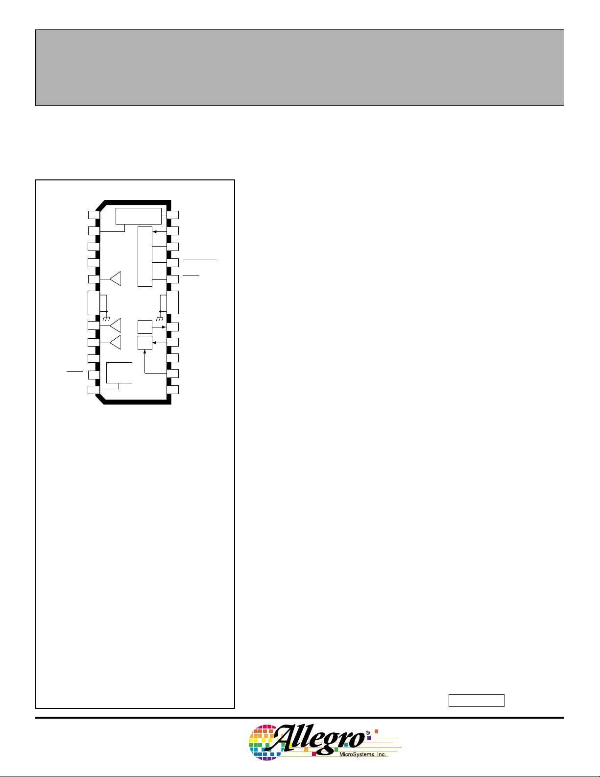
The A8905CLB isw a three-phase brushless dc motor controller/
driver for use with CD-ROM or DVD drives. The three half-bridge
LOAD
SUPPLY
C
D2
C
WD
C
ST
OUT
GROUND
GROUND
OUT
OUT
CENTERTAP
BRAKE
C
RES
A
B
C
1
2
3
4
5
6
7
8
9
9
10
11
V
BB
BOOST
CHARGE
PUMP
COMMUTATION
DELAY
SERIAL PORT
MUX
FLL
C
24
D1
23
DATA IN
22
CLOCK
21
CHIP SELECT
20
RESET
19
GROUND
18
GROUND
DATA OUT
17
OSCILLATOR
16
LOGIC
V
15
DD
SUPPLY
INDEX
14
1312
FILTER
Dwg. PP-040-1
ABSOLUTE MAXIMUM RATINGS
at T
= +25°C
A
Load Supply Voltage, VBB. . . . . . 14 V
Output Current, I
Logic Supply Voltage, V
. . . . . . . . ±1.25 A
OUT
. . . . 6.0 V
DD
Logic Input Voltage Range,
. . . . . . . -0.3 V to VDD + 0.3 V
V
IN
Package Power Dissipation,
. . . . . . . . . . . . . . . . See Graph
P
D
Operating Temperature Range,
. . . . . . . . . . . . . . 0°C to +70°C
T
A
Junction Temperature, T
. . . +150°C†
J
Storage Temperature Range,
. . . . . . . . . . . . -55°C to +150°C
T
S
† Fault conditions that produce excessive
junction temperature will activate device thermal
shutdown circuitry. These conditions can be
tolerated, but should be avoided.
DISCONTINUED PRODUCT
Output current rating may be restricted to a value
determined by system concerns and factors.
These include: system duty cycle and timing,
ambient temperature, and use of any heatsinking
and/or forced cooling. For reliable operation, the
specified maximum junction temperature should
not be exceeded.
— FOR REFERENCE ONLY
outputs are low on-resistance n-channel DMOS devices capable of
driving up to 1.25 A. The A8905CLB provides complete, reliable,
self-contained back-EMF sensing motor startup and running algorithms.
A programmable digital frequency-locked loop speed control circuit
together with the linear current control circuitry provides precise motor
speed regulation.
A serial port allows the user to program various features and modes
of operation, such as the speed control parameters, startup current limit,
sleep mode, diagnostic modes, and others.
APPLICATIONS
■ CD-ROMs
■ DVDs
FEATURES
■ DMOS Outputs
■ Low r
■ Startup Commutation Circuitry
■ Back-EMF Commutation Circuitry
■ Serial Port Interface
■ Frequency-Locked Loop Speed Control
■ Tachometer Signal Input
■ Programmable Start-Up Current
■ Diagnostics Mode
■ Sleep Mode
■ Linear Current Control
■ Internal Current Sensing
■ Dynamic Braking Through Serial Port
■ Power-Down Dynamic Braking
■ System Diagnostics Data Out
■ Data Out Ported in Real Time
■ Internal Thermal Shutdown Circuitry
Always order by complete part number, e.g., A8905CLB .
DS(on)
Page 2
8905
3-PHASE BRUSHLESS DC
MOTOR CONTROLLER/DRIVER
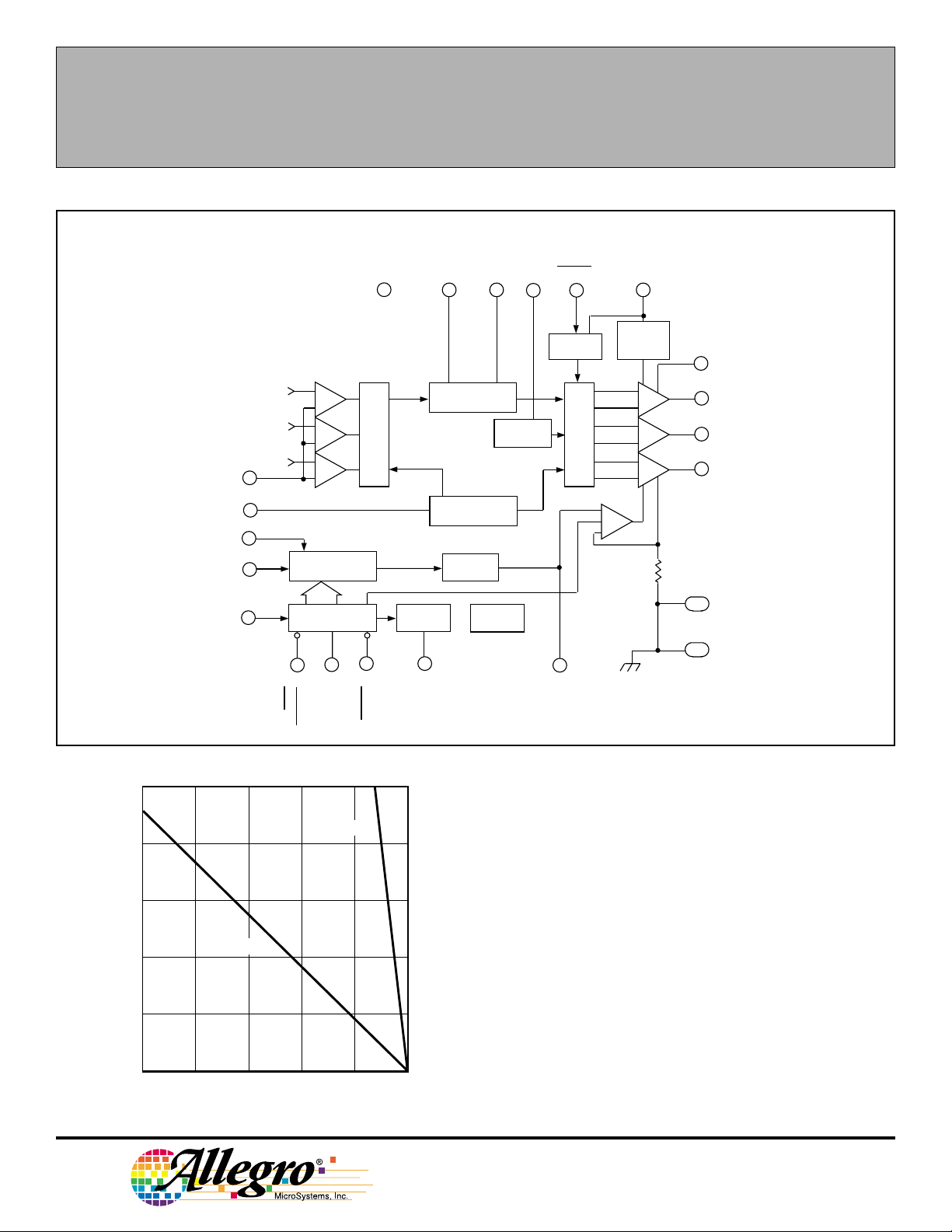
FUNCTIONAL BLOCK DIAGRAM
CENTERTAP
C
WD
INDEX
OSC
DATA IN
14
23
10
16
OUT
OUT
OUT
3
LOGIC
SUPPLY
A
B
C
FREQUENCY-
LOCKED LOOP
SERIAL PORT MUX
CHIP
SELECT
2221
CLOCK
COMMUTATION
RESET
15
V
DD
LOGIC
FCOM
BLANK
1720
C
D1
24 2
COMMUTATION
DELAY
WATCHDOG
TIMER
CHARGE
PUMP
OUT
DATA
C
D2
START-UP
OSC.
TSD
C
ST
4
BRAKE
BRAKE
13
FILTER
11
LOGIC
SEQUENCE
CURRENT
CONTROL
C
RES
12
BOOST
CHARGE
PUMP
V
BB
R
LOAD
1
SUPPLY
5
OUT
A
8
OUT
B
9
OUT
C
S
6-7
GROUND
18-19
GROUND
Dwg. FP-034-1
2.5
R = 6°C/W
θJT
2.0
1.5
R = 55°C/W
1.0
θJA
0.5
0
25
ALLOWABLE PACKAGE POWER DISSIPATION in WATTS
50 75 100 125 150
TEMPERATURE in °C
Dwg. GP-019B
115 Northeast Cutoff, Box 15036
Worcester, Massachusetts 01615-0036 (508) 853-5000
Copyright © 1998 Allegro MicroSystems, Inc.
Page 3

8905
3-PHASE BRUSHLESS DC
MOTOR CONTROLLER/DRIVER
ELECTRICAL CHARACTERISTICS at T
= +25°C, V
A
= 5.0 V
DD
Limits
Characteristic Symbol Test Conditions Min. Typ. Max. Units
Logic Supply Voltage V
Logic Supply Current I
DD
DD
Operating 4.5 5.0 5.5 V
Operating — 7.5 10 mA
Sleep Mode — — 1.5 mA
Load Supply Voltage V
Thermal Shutdown T
Thermal Shutdown Hys. ∆T
BB
J
J
Operating 4.5 — 14 V
— 165 — °C
—20—°C
Output Drivers
Output Leakage Current I
Total Output ON Resistance r
Output Sustaining Voltage V
DS(on)
DS(sus)
Clamp Diode Forward Voltage V
DSX
F
VBB = 14 V, V
VBB = 14 V, V
I
= 600 MA — 1.1 1.4 Ω
OUT
V
= 14 V, I
BB
= 14 V — 1.0 300 µA
OUT
= 0 V — -1.0 -300 µA
OUT
= I
OUT
(MAX), L = 3 mH 14 — — V
OUT
IF = 1.0 A — 1.25 1.5 V
Control Logic
Logic Input Voltage V
Logic Input Current I
DATA Output Voltage V
V
CST Current I
IN(0)
V
IN(1)
IN(0)
I
IN(1)
OUT(0)
OUT(1)
CST
INDEX, RESET, CLK, -0.3 — 1.5 V
CHIP SELECT, OSC, BRAKE 3.5 — 5.3 V
V
= 0 V — — -0.5 µA
IN
V
= 5.0 V — — 1.0 µA
IN
I
= 500 µA — — 1.5 V
OUT
I
= -500 µA 3.5 — — V
OUT
Charging 14 20 28 µA
Discharging -14 -20 -28 µA
CST Threshold V
Filter Current I
CSTH
V
CSTL
FILTER
Charging 7.0 10 15 µA
2.1 2.5 2.9 V
— 500 — mV
Discharging -7.0 -10 -15 µA
CD Current I
CD
Leakage, V
Charging 14 22 28 µA
= 2.5 V — 5.0 — nA
FILTER
Discharging -26 -35 -66 µA
CD Current Matching — I
CD Threshold V
CWD Current I
CD
CWD
CD(DISCHRG)/ICD(CHRG)
Charging 14 22 28 µA
1.7 2.2 2.3 —
— 2.5 — V
Continued next page …
Page 4
8905
3-PHASE BRUSHLESS DC
MOTOR CONTROLLER/DRIVER
ELECTRICAL CHARACTERISTICS continued
Limits
Characteristic Symbol Test Conditions Min. Typ. Max. Units
CWD Threshold Voltage V
Max. FLL Oscillator Frequency f
I
(MAX) Accuracy — I
OUT
BRAKE Threshold V
Transconductance Gain g
Centertap Resistors R
V
OSC
TL
TH
BRK
m
CT
Back-EMF Hysteresis — V
VDD = 5.1 V, T
VDD = 4.5 V, T
= 1 A — ±20 — %
OUT
- V
BEMF
= 25°C20——MHz
A
= 70°C—10—MHz
A
at 152540mV
CTAP
FCOM Transition -15 -25 -40 mV
0.80 0.85 0.95 V
2.4 2.75 3.0 V
1.4 1.7 2.0 V
0.26 0.35 0.50 A/V
5.0 10 13 kΩ
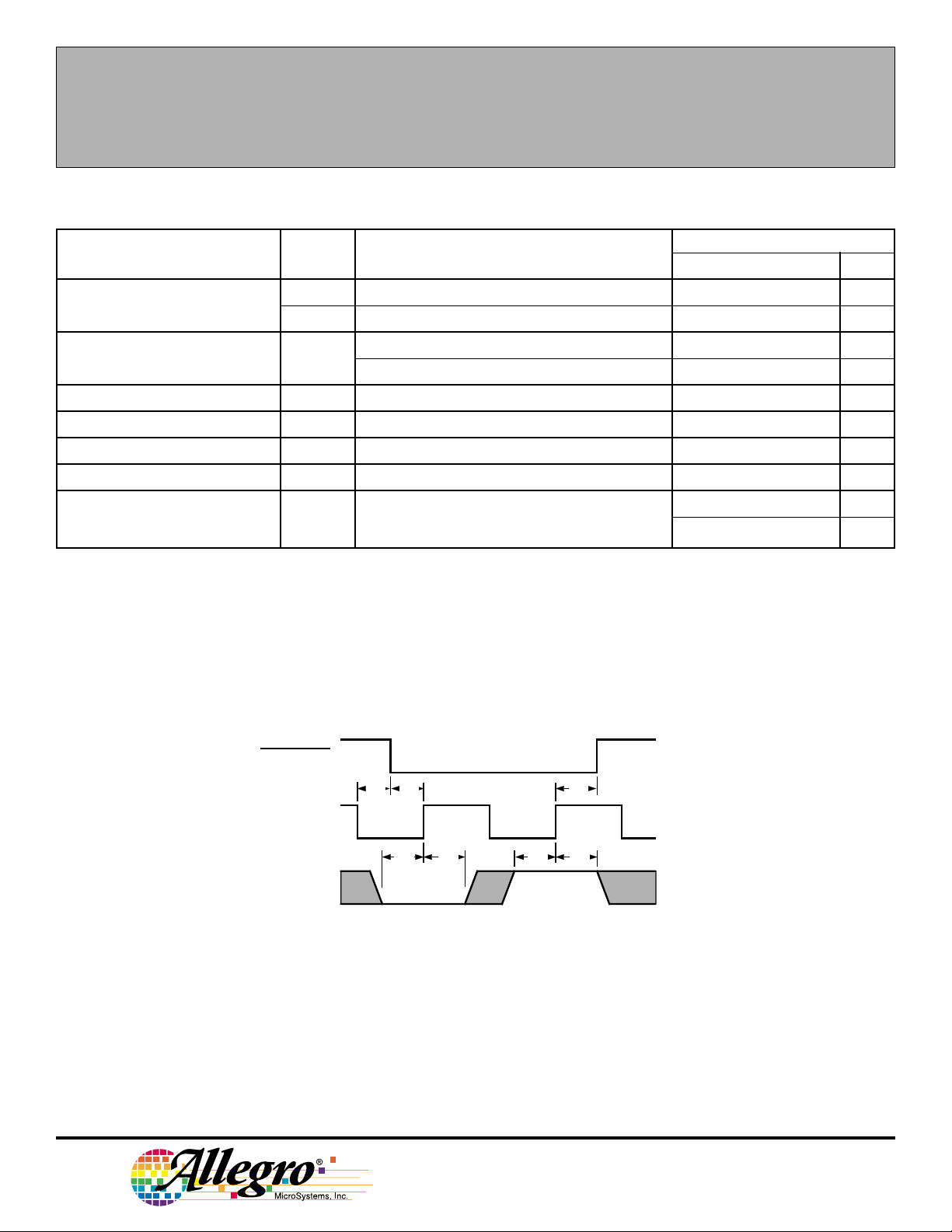
SERIAL PORT TIMING CONDITIONS
CHIP SELECT
A
E
CLOCK
C
D C D
DATA
A. Minimum CHIP SELECT setup time before CLOCK rising edge ...... 100 ns
B. Minimum CHIP SELECT hold time after CLOCK rising edge ........... 150 ns
C. Minimum DATA setup time before CLOCK rising edge .................... 150 ns
D. Minimum DATA hold time after CLOCK rising edge ........................ 150 ns
E. Minimum CLOCK low time before CHIP SELECT .............................. 50 ns
F. Maximum CLOCK frequency........................................................... 3.3 MHz
B
Dwg. WP-019
115 Northeast Cutoff, Box 15036
Worcester, Massachusetts 01615-0036 (508) 853-5000
Page 5

8905
3-PHASE BRUSHLESS DC
MOTOR CONTROLLER/DRIVER
TERMINAL FUNCTIONS
Term. Terminal Name Function
1 LOAD SUPPLY VBB; the 5 V or 12 V motor supply.
2C
3C
4CSTStartup oscillator timing capacitor.
5 OUT
6-7 GROUND Power and logic ground and thermal heat sink.
8 OUT
9 OUT
10 CENTERTAP Motor centertap connection for back-EMF detection circuitry.
11 BRAKE Active low turns ON all three sink drivers shorting the motor windings to ground. External
12 C
13 FILTER Analog voltage input to control motor current. Also, compensation node for internal speed
14 INDEX External tachometer input.
15 LOGIC SUPPLY VDD; the 5 V logic supply.
16 OSCILLATOR Clock input for the speed reference counter. Typical max. frequency is 10 MHz.
17 DATA OUT Thermal shutdown indicator, FCOM, TACH, or SYNC signals available in real time,
18-19 GROUND Power and logic ground and thermal heat sink.
20 RESET When pulled low forces the chip into sleep mode; clears all serial port bits.
21 CHIP SELECT Strobe input (active low) for data word.
22 CLOCK Clock input for serial port.
23 DATA IN Sequential data input for the serial port.
24 C
D2
WD
A
B
C
RES
D1
One of two capacitors used to generate the ideal commutation points from the back-EMF
zero-crossing points.
Timing capacitor used by the watchdog circuit to disable the back-EMF comparators
during commutation transients, and to detect incorrect motor position.
Power amplifier output A to motor.
Power amplifier output B to motor.
Power amplifier output C to motor.
capacitor and resistor at BRAKE provide brake delay. The brake function can also be
controlled via the serial port.
External reservoir capacitor used to hold charge to drive the source drivers’ gates. Also
provides power for brake circuit.
control loop.
controlled by 2-bit multiplexer in serial port.
One of two capacitors used to generate the ideal commutation points from the back-EMF
zero-crossing points.
Page 6

8905
3-PHASE BRUSHLESS DC
MOTOR CONTROLLER/DRIVER
FUNCTIONAL DESCRIPTION
Power Outputs. The power outputs of the
A8905CLB are n-channel DMOS transistors with
a total source plus sink r
of typically 1.1 Ω.
DS(on)
Internal charge pump boost circuitry provides
voltage above supply for driving the high-side
DMOS gates. Intrinsic ground clamp and flyback
diodes provide protection when switching inductive loads and may be used to rectify motor backEMF in power-down conditions. An external
Schottky power diode or pass FET is required in
series with the load supply to allow motor backEMF rectification in power-down conditions.
Back-EMF Sensing Motor Startup and
Running Algorithm. The A8905CLB provides a
complete self-contained back-EMF sensing startup
and running commutation scheme. The three halfbridge outputs are controlled by a state machine.
There are six possible combinations. In each state,
one output is high (sourcing current), one low
(sinking current), and one is OFF (high impedance
or ‘Z’). Motor back EMF is sensed at the OFF
output. The truth table for the output drivers
sequencing is:
Sequencer
State OUT
A
OUT
B
OUT
C
1 High Low Z
2 Z Low High
3 Low Z High
4 Low High Z
5 Z High Low
6 High Z Low
At startup, the outputs are enabled in one of
the sequencer states shown. The back EMF is
examined at the OFF output by comparing the
output voltage to the motor centertap voltage at
CENTERTAP. The motor will then either step
forward, step backward, or remain stationary (if in
a null-torque position). If the motor moves, the
back-EMF detection circuit waits for the correct
polarity back-EMF zero crossing (output crossing
through centertap). True back-EMF zero crossings are used by the adaptive commutation delay
circuit to advance the state sequencer (commutate)
at the proper time to synchronously run the motor.
Back-EMF zero crossings are indicated by FCOM, an internal signal that
toggles at every zero crossing. FCOM is available at the DATA OUT terminal
via the programmable data out multiplexer.
V
OUTA
V
OUTB
V
OUTC
FCOM
V
SOURCE ON
CTAP
BACK-EMF VOLTAGE
SINK ON
FCOM TOGGLES AT
BACK-EMF ZERO CROSSING
Dwg. WP-016-1
Startup Oscillator. If the motor does not move at the initial startup state,
then it is in a null-torque position. In this case, the outputs are commutated
automatically by the startup oscillator after a period set by the external
capacitor at CST.
V
CSTH
V
CST
V
CSTL
t
CST
V
CWD
Dwg. WP-020
where t
CST
=
4(V
I
ST(charge)
CSTH
- V
+ I
CSTL
) x C
ST(discharge)
ST
In the next state, the motor will move, back EMF will be detected, and the
motor will accelerate synchronously. Once normal synchronous back-EMF
commutation occurs, the startup oscillator is defeated by pulses of pulldown
current at CST at each commutation, which prevents CST from reaching its
upper threshold and thus completing a cycle and commutating.
115 Northeast Cutoff, Box 15036
Worcester, Massachusetts 01615-0036 (508) 853-5000
Page 7

8905
Dwg. WP-022
3-PHASE BRUSHLESS DC
MOTOR CONTROLLER/DRIVER
Adaptive Commutation Delay. The
adaptive commutation delay circuit uses the
back-EMF zero-crossing indicator signal
(FCOM) to determine an optimal commutation
time for efficient synchronous operation. This
circuit commutates the outputs, delayed from the
last zero crossing, using two external timing
capacitors, CD1 and CD2, to measure the time
between crossings.
t
FCOM
FCOM
V
CWD
t
CD1
V
CD1
t
CD2
V
CD2
capacitors, the voltage excursion should be 1.5 V to 2.5 V at rated speed.
Solving for C in the equation I = Cdv/dt, where dv = 2.5 V, I = 22 µA, and
dt = t
FCOM
20/RPM
=
#motor poles
Use of a capacitor slightly greater than this value will ensure that the commutation delay capacitors never charge to the high rail.
Blanking and Watchdog Timing Functions. The blanking and watchdog
timing functions are derived from one timing capacitor, CWD.
where t
BLANK
and tWD =
=
VTL x C
VTH x C
I
CWD
I
WD
WD
CWD
The CWD capacitor begins charging at each commutation, initiating the
BLANK signal. BLANK is an internal signal that inhibits the back-EMF
comparators during the commutation transients, preventing errors due to
inductive recovery and voltage settling transients.
V
TL
V
CWD
t
BLANK
BLANK
Dwg. WP-016-2
I
where tCD = t
FCOM
x
CD(charge),
[I
CD(discharge)
]
CD1 charges up with a fixed current from its
2.5 V reference while FCOM is high. When
FCOM goes low at the next zero crossing, CD1 is
discharged at approximately twice the charging
current. When CD1 reaches the CD threshold, a
commutation occurs. CD2 operates similarly
except on the opposite phase of FCOM . Thus
the commutations occur approximately halfway
between zero crossings. The actual delay is
slightly less than halfway to compensate for
electrical delays in the motor, which improves
efficiency.
Because the commutation-delay capacitors
are adaptive in nature, the absolute value and
tolerance is not critical. In choosing these
V
CWD
BLANK
NORMAL COMMUTATION
V
V
TL
t
BLANK
t
WD
Dwg. WP-021
WATCHDOG-TRIGGERED COMMUTATION
TH
Page 8

8905
3-PHASE BRUSHLESS DC
MOTOR CONTROLLER/DRIVER
The watchdog timing function allows time to detect correct motor position
by checking the back-EMF polarity after each commutation. If the correct
polarity is not observed between t
and tWD, then the watchdog timer
BLANK
commutates the outputs to the next state to synchronize the motor. This
function is useful in preventing excessive reverse rotation, and helps in
resynchronizing (or starting) with a moving spindle.
Current Control. The A8905CLB provides linear current control via the
FILTER terminal, an analog voltage input. Maximum current limit is also
provided, and is controlled in four steps via the serial port. Output current is
sensed via an internal sense resistor (RS). The voltage across the sense resistor
is compared to one-tenth the voltage at the FILTER terminal less two diode
drops, or to the maximum current limit reference, whichever is lower. This
transconductance function is I
OUT
= (V
-2VD) / 10RS, where RS is
FILTER
nominally 0.3 Ω and VD is approximately 0.7 V.
YANK
S Q
R
SPEED-CONTROL
INITIALIZATION
+
x1
–
1.85 V
ERROR FAST
SEQUENTIAL
LOGIC
V
C
RES
BOOST
CHARGE
V
DD
MUX
–
+
I
V max
FROM
SERIAL PORT
REGISTER
D3 AND D4
PUMP
÷10
LINEAR
CURRENT CONTROL
+
–
BB
OUT
R
S
Dwg. EP-046
ERROR SLOW
FROM FLL
C
F1
R
F1
POWER UP
ERROR FAST
FROM FLL
FILTER
C
F2
CHARGE
V
DD
I
c
I
d
Speed Control. The A8905CLB includes a frequency-locked loop speed
control system. This system monitors motor speed via internal or external
digital tachometer signals, generates a precision speed reference, determines
the digital speed error, and corrects the motor current via an internal charge
pump and external filtering components on the FILTER terminal.
A once-per-revolution TACH signal can be
generated by counting cycles of FCOM (the
number of motor poles must be selected via the
serial port). TACH is then a jitter-free signal that
toggles once per motor revolution. The rising
edge of TACH triggers REF, a precision speed
reference derived by a programmable counter.
The duration of REF is set by programming the
counter to count the desired number of OSC
cycles
desired
total count
=
desired motor speed (rpm)
60 x f
OSC
where the total count (number of oscillator cycles)
is equal to the sum of the selected (programmed
low) count numbers corresponding to bits D5
through D18.
The speed error is detected as the difference
in falling edges of TACH and REF. The speed
error signals control the error-correcting charge
pump on the FILTER terminal, which drive the
external loop compensation components to correct
the motor current.
Index. An external tachometer signal may be
used to create the TACH signal, rather than the
internally derived once around. To use this mode,
the signal is input to the INDEX terminal, and the
index mode must be enabled via the serial port.
When Switching from the once-around mode to
index mode, it is important to monitor the SYNC
signal on DATA OUT, and switch modes only
when SYNC is low. This ensures making the
transition without disturbing the speed control
loop. The speed reference counter should be
reprogrammed at the same time.
FCOM
OSC
SECTOR
COUNT
(3 x MOTOR POLES)
D20 &
D21
4-BIT
FIXED
COUNTER
ONCE-AROUND
PULSE
SERIAL PORT
REGISTER
D5–D18
14-BIT
PROGRAMMABLE
COUNTER
D19
MUX
REF
Speed Loop Initialization (YANK). To
improve the acquire time of the speed control
÷2
TACH
loop, there is an automatic feature controlled by an
internal YANK signal. The motor is started at the
maximized programmed current by bypassing the
REF
TACH
ERROR
SLOW
REF
TACH
ERROR
FAST
Dwg. EP-045
115 Northeast Cutoff, Box 15036
Worcester, Massachusetts 01615-0036 (508) 853-5000
FILTER terminal. The FILTER terminal is
clamped to two diodes above ground, initializing it
near the closed loop operating point. YANK is
enabled at startup and stays high until the desired
speed is reached. Once the first error-fast occurs,
indicating the motor crossed through the desired
speed, YANK goes low. This releases the clamp
on the FILTER terminal and current control is
returned to FILTER. This feature optimizes speed
Page 9

8905
3-PHASE BRUSHLESS DC
MOTOR CONTROLLER/DRIVER
acquire and minimizes settling. The Current Control Block Diagram illustrates
the YANK signal and its effects.
Braking. A dynamic braking feature of the A8905CLB shorts the three
motor windings to ground. This is accomplished by turning the three source
drivers OFF and the three sink drivers ON. Activation of the brake can be
implemented through the BRAKE input or through the D2 bit in the serial port.
The supply voltage for the brake circuitry is the C
voltage, allowing the brake
RES
function to remain active after power failure. Power-down braking with delay can
be implemented by using an external RC and other components to control the
brake terminal, as shown. Brake delay can be set using the equation below to
ensure that voice-coil head retract occurs before the spindle motor brake is
activated. Once the brake is activated, due to the inherent capacitive input, the
three sink drivers will remain active until the device is reset.
V
BRK
V
FAULT - VD
FAULT D
24
23
22
21
SERIAL PORT
20
19
BRAKE
ACTIVATED
t
BRK
DATA IN
CLOCK
CHIP SELECT
RESET
V
Dwg. OP-004
C
D1
BRK
TYPICAL
FAULT
V
RET
BYPASS
t
= RBCB 1 – l
BRK
C
B
R
B
V
BB
1
V
2
C
D2
3
C
WD
4
C
ST
5
6
BRAKE
COMMUTATION
BB
n
V – V
DELAY
APPLICATION
18
BYPASS
17
16
V
15
DD
14
1312
INDEX
+5 V
DATA OUT
OSC (REF)
R
F1
C
F2
Dwg. EP-036-1
C
F1
FAULT
7
8
9
9
10
BOOST
CHARGE
B
C
RES
0.22 µF
11
PUMP
C
R
B
MUX
FLL
Centertap. The A8905CLB internally
simulates the centertap voltage of the motor.
To obtain reliable start-up performance from
motor to motor, the motor centertap should be
connected to this terminal.
Serial Port. The serial port functions to
write various operational and diagnostic modes
to the A8905CLB. The serial port DATA IN is
enabled/disabled by the CHIP SELECT
terminal. When CHIP SELECT is high the
serial port is disabled and the chip is not
affected by changes in data at the DATA IN or
CLOCK terminals.
To write data to the serial port, the
CLOCK terminal should be low prior to the
CHIP SELECT terminal going low. Once
CHIP SELECT goes low, information on the
DATA IN terminal is read into the shift register
on the positive-going transition of the CLOCK.
There are 24 bits in the serial input port.
Data written into the serial port is latched
and becomes active upon the low-to-high
transition of the CHIP SELECT terminal at the
end of the write cycle. D0 will be the last bit
written to the serial port.
Reset. The RESET terminal (when pulled
low) clears all serial port bits, including the D0
latch, which puts the A8905CLB in the sleep
mode.
Page 10

8905
3-PHASE BRUSHLESS DC
MOTOR CONTROLLER/DRIVER
SERIAL PORT BIT DEFINITIONS
D0- Sleep/Run Mode; LOW = Sleep, HIGH = Run
This bit allows the device to be powered down when not in
use.
D1- Step Mode; LOW = Normal Operation, HIGH = Step Only
When in the step-only mode the back-EMF commutation
circuitry is disabled and the power outputs are commutated
by the start-up oscillator. This mode is intended for device
and system testing.
D2- Brake; LOW = Run, HIGH = Brake.
D3 and D4-These two bits set the output current limit:
D3 D4 Current Limit
0 0 Saturated
01 1 A
1 0 800 mA
1 1 600 mA
D5 thru D18-This 14-bit word (active low) programs the REF time
to set desired motor speed.
Bit Number Count Number
D19-Speed-control mode switch;
LOW = internal once-around speed signal,
HIGH = external index data.
D20 and D21-These bits program the number of motor poles
for the once-around FCOM counter:
D20 D21 Motor Poles
00 8
01 –
10 16
11 12
D22 and D23-Control the multiplexer for DATA OUT:
D22 D23 Data Out
0 0 TACH (once around or index)
0 1 Thermal Shutdown
1 0 SYNC
1 1 FCOM
D5 16
D6 32
D7 64
D8 128
D9 256
D10 512
D11 1 024
D12 2 048
D13 4 096
D14 8 192
D15 16 384
D16 32 768
D17 65 536
D18 131 072
115 Northeast Cutoff, Box 15036
Worcester, Massachusetts 01615-0036 (508) 853-5000
Page 11

8905
°
°
3-PHASE BRUSHLESS DC
MOTOR CONTROLLER/DRIVER
Dimensions in Inches
(for reference only)
0.2992
0.2914
0.020
0.013
0.0926
0.1043
24 13
1 2
3
0.6141
0.050
0.5985
0.0040 MIN.
Dimensions in Millimeters
(controlling dimensions)
24 13
BSC
NOTE 1
NOTE 3
0.0125
0.0091
0.491
0.394
0.050
0.016
0° TO 8
Dwg. MA-008-25 in
0.32
0.23
7.60
7.40
1 2
0.51
0.33
3
15.60
15.20
2.65
2.35
0.10
MIN
.
NOTES: 1. Webbed lead frame. Leads 6, 7, 18, and 19 are internally one piece.
2. Lead spacing tolerance is non-cumulative.
3. Exact body and lead configuration at vendor’s option within limits shown.
1.27
BSC
NOTE 1
NOTE 3
10.65
10.00
1.27
0.40
0° TO 8
Dwg. MA-008-25A mm
Page 12

8905
3-PHASE BRUSHLESS DC
MOTOR CONTROLLER/DRIVER
Allegro MicroSystems, Inc. reserves the right to make, from time
to time, such departures from the detail specifications as may be
required to permit improvements in the design of its products.
The information included herein is believed to be accurate and
reliable. However, Allegro MicroSystems, Inc. assumes no
responsibility for its use; nor for any infringements of patents or
other rights of third parties which may result from its use.
115 Northeast Cutoff, Box 15036
Worcester, Massachusetts 01615-0036 (508) 853-5000
 Loading...