

Page 1

a8237
®
Programmable
DMA Controller
April 1999, ver. 1.01 Data Sheet
■
a8237
Features
General Description
■
■
■
■
■
■
The
controller, which controls memory-to-peripheral and memory-tomemory data transfers and provides block memory initialization
capability. Four independently programmable channels are available in
the
a8237
Figure 1 shows the symbol for the
Figure 1. a8237 Symbol
MegaCore function implementing a programmable direct
memory access (DMA) controller
Optimized for FLEX® architecture
Provides four independent channels
Offers static read/write or handshaking modes
Includes direct bit set/reset capability
Uses approximately 1,201 FLEX logic elements (LEs)
Functionally based on the Intel 8237A and Harris 82C37A devices,
except as noted in “Variations & Clarifications” on page 24
a8237
MegaCore function implements a programmable DMA
, and DMA requests can be made via hardware or software.
a8237
.
A8237
adstb
clk
hlda
ncs
neopin
niorin
niowin
ready
reset
ain[3..0]
dbin[7..0]
dreq[3..0]
Altera Corporation 5
A-DS-A8237-01.01
aen
dben
dmaenable
hrq
neopout
niorout
niowout
nmemr
nmemw
aout[7..0]
dack[3..0]
dbout[7..0]
Page 2

a8237 Programmable DMA Controller Data Sheet
Table 1 describes the input and output ports of the
function.
Table 1. a8237 Ports (Part 1 of 2)
Name Type Polarity Description
clk
hlda
ncs
neopin
niorin
niowin
ready
reset
ain[3..0]
dbin[7..0]
dreq[3..0]
adstb
aen
dben
dmaenable
hrq
neopout
niorout
Input – Clock. Used to generate and synchronize
Input High Hold acknowledge. This signal from the microprocessor indicates the
release of the system bus to the
Input Low Chip select. When
write transactions to internal registers are enabled.
Input Low End of process. Permits external termination of the current DMA service.
Input Low I/O read control. When
transactions from internal registers are enabled.
Input Low I/O write control. When
asynchronously written into the
Input High Ready. Extends the read and write pulses associated with slow memory
or peripherals. When
returns high.
Input High Reset. Clears the command, status, request, and temporary registers.
Also clears the byte pointer, mode register counter, and the controller
state machine. Sets the mask register so requests are ignored after
initialization.
Input – Register address bus. Selects one of the internal
Table 2 on page 9.
Input – Data bus input. The microprocessor writes data to internal registers via
the
dbin[7..0]
Input – DMA request bus. Programmable polarity. Asynchronous signals from
peripherals requesting DMA service.
Output High Address strobe. Latches the MSB of the DMA address from
dbout[7..0]
Output High Address enable. Enables an external address latch containing the most
significant address byte of a DMA transfer.
Output High Data bus enable. Active when data registers are read. Also active during
DMA transfers, allowing the most significant bit (MSB) of the address to
latch the output of temporary register data during memory-to-memory
writes.
Output High DMA enable. Asserted during an active DMA cycle. Can create
bidirectional signals from the
signals, and the lower four bits of the address bus.
Output High Hold request. Requests control of the system bus.
Output Low End of process. Indicates normal termination of a DMA transfer.
Output Low I/O read output. Read strobe to I/O devices as DMA writes to memory.
ncs
is active, the
niorin
niowin
ready
is low, wait states are inserted until
bus.
into an external address latch.
niorin, niorout, niowin
a8237
a8237
.
a8237
is selected, and read and
is low and the
is low and the
a8237
.
a8237
MegaCore
operations.
a8237
is selected, read
a8237
is selected, data is
a8237
registers. See
, and
ready
niowout
6 Altera Corporation
Page 3

a8237 Programmable DMA Controller Data Sheet
Table 1. a8237 Ports (Part 2 of 2)
Name Type Polarity Description
niowout
nmemr
nmemw
aout[7..0]
dack[3..0]
dbout[7..0]
Output Low I/O write output. Write strobe to I/O devices as DMA reads from memory.
Output Low Memory read. Read strobe to memory elements during DMA reads or
memory-to-memory transfers.
Output Low Memory write. Write strobe to memory elements during DMA writes or
memory-to-memory transfers.
Output – Address output. During DMA service,
significant byte of the DMA address.
Output – DMA acknowledge bus. Programmable polarity. Indicates a DMA cycle
has been granted to the peripheral.
Output – Data bus output. The microprocessor reads data from internal registers
via the
dbout[7..0]
of the DMA address and temporary data held during memory-to-memory
transfers.
bus. Also used to output the most significant byte
aout[7..0]
comprises the least
Altera Corporation 7
Page 4
a8237 Programmable DMA Controller Data Sheet
Functional
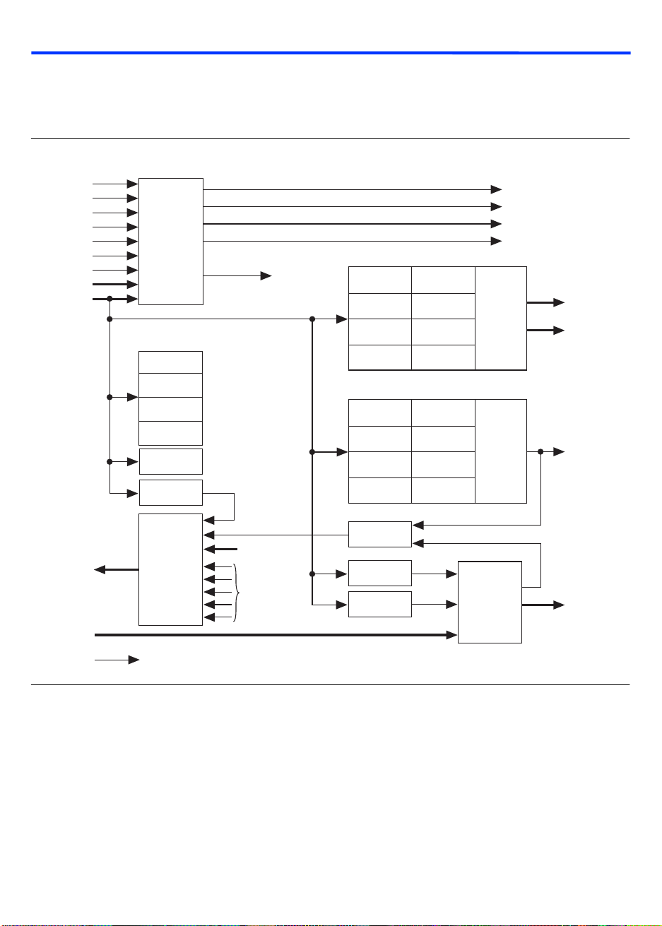
Figure 2 shows a block diagram of the
Description
Figure 2. a8237 Block Diagram
hlda
ncs
neopin
niorin
niowin
ready
reset
ain[3..0]
dbin[7..0]
Control
Logic
(State Machine
and Decoder)
Mode
Registers
Channel 0
Channel 1
Channel 2
Channel 3
Command
Register
Temporary
Register
Internal
Control
Signals
a8237
DMA Address Registers
Channel 0
Base
Channel 1
Base
Channel 2
Base
Channel 3
Base
Channel 0
Base
Channel 1
Base
Channel 2
Base
Channel 3
Base
Channel 0
Current
Channel 1
Current
Channel 2
Current
Channel 3
Current
DMA Word Count Registers
Channel 0
Current
Channel 1
Current
Channel 2
Current
Channel 3
Current
MegaCore function.
hrq, aen, adstb
niorout, niowout
nmemr, nmemw
dben, dmaenable, neopout
Temporary
Register
Temporary
Register
aout[7..0]
aout[15..8]
to dbout[7..0]
to
Control
Logic
Status
Register
Request
Register
Mask
Register
Request
Priority
Encoder
dack[3..0]
dbout[7..0]
dreq[3..0]
clk
Data
Output
Multiplexer
aout[15..8]
Other
Registers
Programming
Several registers in the
can be executed. However, to avoid unpredictable behavior, disable the
DMA cycles during programming by setting bit 2 of the command
register.
8 Altera Corporation
a8237
must be programmed before DMA cycles
Page 5

a8237 Programmable DMA Controller Data Sheet
The microprocessor can program the
ain[3..0]
bus are asserted. When
the microprocessor writes data to internal registers via the
bus. When
niorin
and
ain[3..0]
data from internal registers via the
a8237
niowin
when the
and
ncs
ain[3..0]
input and the
are asserted,
dbin[7..0]
are asserted, the microprocessor reads
dbout[7..0]
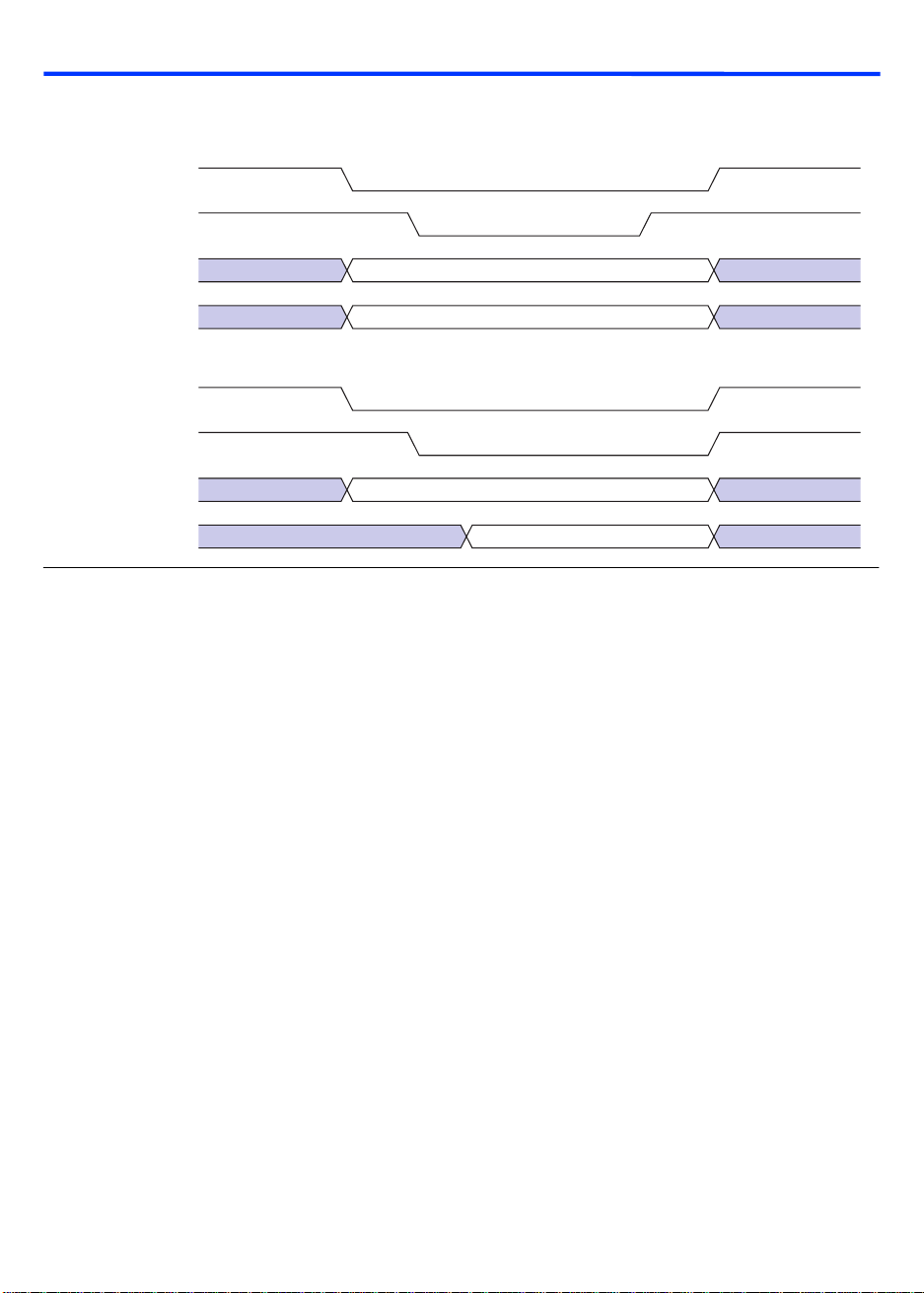
bus. See “Host Processor
Write Timing” and “Host Processor Read Timing” in Figure 3.
The byte pointer bit must be toggled to the correct value before operating
on the DMA address register and word count register. The set byte
pointer and clear mode register counter commands can change the
contents of registers, effectively acting as write commands.
Register Address Map
Table 2 shows the register address map for the
Table 2. Register Address Map
ain3 ain2 ain1 ain0 Channel Write
0 0 0 0 0 Base and current DMA address register Current DMA address register
0 0 0 1 Base and current DMA word count register Current DMA word count register
0 0 1 0 1 Base and current DMA address register Current DMA address register
0 0 1 1 Base and current DMA word count register Current DMA word count register
0 1 0 0 2 Base and current DMA address register Current DMA address register
0 1 0 1 Base and current DMA word count register Current DMA word count register
0 1 1 0 3 Base and current DMA address register Current DMA address register
0 1 1 1 Base and current DMA word count register Current DMA word count register
1 0 0 0
1 0 0 1
1 0 1 0
1 0 1 1
1 1 0 0
1 1 0 1
1 1 1 0
1 1 1 1
Command register Status register
X
X Single request bit command Request register
X Single mask bit command Command register
X Mode register Mode register
X Clear byte pointer command Set byte pointer command
X Master clear command Temporary register
X Clear mask register command Clear mode register counter
X Mask register Mask register
(1), (2)
a8237.
Read
(1), (2)
Notes:
(1) If the byte pointer is set to 0, the byte pointer flag selects the least significant byte.
If the byte pointer is set to 1, the byte pointer flag selects the most significant byte.
The byte pointer flag is a single-bit internal register that selects either the least significant or most significant byte
of the 16-bit registers in the a8237, allowing the microprocessor to write and read via the 8-bit data bus. See “Clear
Byte Pointer Command” and “Set Byte Pointer Command” on page 17 for more information.
(2) The X indicates “don’t care.”
Altera Corporation 9
Page 6

a8237 Programmable DMA Controller Data Sheet
Registers
The a8237 MegaCore function contains the following registers:
■ Base address
■ Current address
■ Base word count
■ Current word count
■ Command
■ Mode
■ Request
■ Mask
■ Status
■ Temporary
Base Address Register
Each of the four DMA channels has a base address register, which is a
16-bit register that contains the starting address for DMA transfers. If
auto-initialization is enabled, the a8237 loads the base address value into
the current address register at the conclusion of a DMA cycle. The
microprocessor writes to the base address register in two parts via
dbin[7..0], and simultaneously loads the current address register. The
byte pointer flag chooses either the least significant or most significant
byte. The microprocessor cannot read the base address register.
Current Address Register
Each of the four DMA channels has a current address register, which is a
16-bit register containing the working address value for DMA transfers.
The microprocessor loads the current address register simultaneously
with the base address register via dbin[7..0]. If auto-initialization is
enabled, the a8237 reloads the base address value at the conclusion of a
DMA cycle. The microprocessor reads or writes to the current address
register in two parts via the 8-bit data bus. The byte pointer flag chooses
the least significant or most significant byte. After each DMA transfer, the
current address value is updated with the incremented or decremented
value from the temporary address register (except for channel 0 in
memory-to-memory mode when the address can be held constant).
10 Altera Corporation
Page 7

a8237 Programmable DMA Controller Data Sheet
Base Word Count Register
Each of the four DMA channels has a base word count register, which is a
16-bit register containing the beginning word count for DMA transfers. If
auto-initialization is enabled, the a8237 loads the base word count value
into the current word count register at the conclusion of a DMA cycle. The
microprocessor writes to the base word count register in two parts via
dbin[7..0], and simultaneously loads the current word count register.
The byte pointer flag chooses the least significant or most significant byte.
The microprocessor cannot read the base word count register.
Current Word Count Register
Each of the four DMA channels has a current word count register, which
is a 16-bit register containing the working word count value for DMA
transfers. The microprocessor loads the current word count value
simultaneously with the base word count register via dbin[7..0]. If
auto-initialization is enabled, the a8237 reloads the base word count
value at the conclusion of a DMA cycle. The microprocessor reads or
writes to the current word count register in two parts via the 8-bit data
bus. The byte pointer flag chooses the least significant or most significant
byte. After each DMA transfer, the current word count value is updated
with the decremented value from the temporary word count register. A
terminal count flag is generated when the count rolls over from zero to
hexadecimal FFFF. The number of DMA transfers is one more than the
value written to the current word count register. For example, if a 16-word
transfer is desired, the word count should be hexadecimal 000F.
Command Register
The command register configures the operation of the a8237, such as
dreq and dack polarity, request priority, function enables/disables, and
transfer timing. The microprocessor reads from or writes to the command
register via the 8-bit data bus. The reset input or a master clear command
clears the command register. See Table 3.
Altera Corporation 11
Page 8

a8237 Programmable DMA Controller Data Sheet
Table 3. Command Register Format
Bit Description
0 0 = Memory-to-memory disable
1 0 = Channel 0 address hold disable
2 0 = Controller enable
3 0 = Normal timing
4 0 = Fixed priority
5 0 = Late write
6 0 = dreq active high
7 0 = dack active low
1 = Memory-to-memory enable
1 = Channel 0 address hold enable
X if bit 0 = 0,
1 = Controller disable
1 = Compressed timing
X if bit 0 = 1,
1 = Rotating priority
1 = Extended write
X if compressed timing,
1 = dreq active low
1 = dack active high
Note (1)
Note (1)
Note (1)
Note:
(1) The X indicates “don’t care.”
Mode Register
The 6-bit mode registers contain the configuration for each of the four
DMA channels. When writing from dbin[7..0], the first two bits of the
mode register format selects the DMA channel mode register. Before
reading each of the mode registers, the clear mode register counter
command must be executed. The next read from the mode register
address returns the value from the channel 0 mode register. Subsequent
mode register reads step through the other mode registers in order. See
Table 4.
12 Altera Corporation
Page 9

a8237 Programmable DMA Controller Data Sheet
Table 4. Mode Register Format
Bit Description
1..0 00 = Channel 0 select
01 = Channel 1 select
10 = Channel 2 select
11 = Channel 3 select
11 during Read
3..2 00 = Verify transfer
01 = Write transfer
10 = Read transfer
11 = Illegal
4 0 = Auto-initialization disable
1 = Auto-initialization enable
5 0 = Address increment
1 = Address decrement
7..6 00 = Demand mode select
01 = Single mode select
10 = Block mode select
11 = Unused (Cascade mode is not supported.)
Request Register
The 4-bit request register allows software DMA requests. Hardware
requests (from dreq inputs) are masked by the mask register values;
software requests generated from the request register are unmaskable.
The request register request bits can only be programmed by the single
request bit command. The reset input or a master clear command clears
the request register. See Table 5.
Table 5. Request Register Format
Bit Description
0 1 = Channel 0 request
1 1 = Channel 1 request
2 1 = Channel 2 request
3 1 = Channel 3 request
7..4 1111
Altera Corporation 13
Page 10

a8237 Programmable DMA Controller Data Sheet
Mask Register
The 4-bit mask register can be set to disable an incoming DMA request,
and contains the mask flags for the dreq inputs of each channel. The
microprocessor can read or write to the mask register via the 8-bit data
bus. Also, the microprocessor can write individual bits of the mask
register with the single mask bit command. The reset input or a master
clear command sets all bits in the mask register. See Table 6.
Table 6. Mask Register Format
Bit Description
0 0 = Channel 0 unmasked
1 0 = Channel 1 unmasked
2 0 = Channel 2 unmasked
3 0 = Channel 3 unmasked
7..4 XXXX during write,
1 = Channel 0 masked
1 = Channel 1 masked
1 = Channel 2 masked
1 = Channel 3 masked
Note (1)
1111 during read
Note:
(1) The X indicates “don’t care.”
Status Register
The 8-bit status register contains the status flags of the four DMA
channels. Each DMA channel has a terminal count flag and a request flag.
The terminal count flag indicates that a DMA cycle is complete or has been
terminated by the neopin signal since the last read of the status register.
The request flag indicates the dreq input of a channel is asserted
regardless of the state of the associated mask bit. The status register is
reset by the reset input or the master clear command. The terminal count
flags are reset on each read of the status register. See Table 7.
14 Altera Corporation
Page 11

a8237 Programmable DMA Controller Data Sheet
Table 7. Status Register Format
Bit Description
0 Channel 0 terminal count
1 Channel 1 terminal count
2 Channel 2 terminal count
3 Channel 3 terminal count
4 Channel 0 request
5 Channel 1 request
6 Channel 2 request
7 Channel 3 request
Temporary Register
The 8-bit temporary register holds the data value for memory-to-memory
DMA transfers. Reading this register from the microprocessor via
dbout[7..0] yields the last data value transferred during the most recent
memory-to-memory DMA cycle. The temporary register cannot be
written to directly by the microprocessor via dbin[7..0], but can be
cleared by the reset input or a master clear command.
Commands
The a8237 MegaCore function can perform the following commands:
■ Single request bit command
■ Single mask bit command
■ Clear byte pointer command
■ Set byte pointer command
■ Master clear command
■ Clear mask register command
■ Clear mode register counter command
These commands are issued by performing either a read or write
operation with a specific address on ain[3..0]. Table 2 on page 9 shows
how to issue these commands.
Altera Corporation 15
Page 12

a8237 Programmable DMA Controller Data Sheet
Single Request Bit Command
The single request bit command alters a single bit of the 4-bit request
register. See Table 8.
Table 8. Single Request Bit Command Format
Bit Description
1..0 00 = Channel 0 select
2 0 = Reset request bit
7..3 XXXXX during write,
Note:
(1) The X indicates “don’t care.”
Single Mask Bit Command
The single mask bit command alters a single bit of the 4-bit mask register.
See Table 9.
01 = Channel 1 select
10 = Channel 2 select
11 = Channel 3 select
1 = Set request bit
Note (1)
Table 9. Single Mask Bit Command Format
Bit Description
1..0 00 = Channel 0 mask bit select
01 = Channel 1 mask bit select
10 = Channel 2 mask bit select
11 = Channel 3 mask bit select
2 0 = Reset mask bit
1 = Set mask bit
7..3 XXXXX during write,
Note:
(1) The X indicates “don’t care.”
16 Altera Corporation
Note (1)
Page 13

a8237 Programmable DMA Controller Data Sheet
Clear Byte Pointer Command
The byte pointer is a single-bit internal register that selects either the least
significant or most significant byte of the 16-bit registers in the a8237. The
byte pointer allows microprocessor write and read operations via the 8-bit
data bus. The clear byte pointer command is a write command that resets
the byte pointer, allowing subsequent access to the least significant byte
of any 16-bit register. The data bus value for the clear byte pointer
command is ignored. The reset input and the master clear command
resets the byte pointer.
Set Byte Pointer Command
The set byte pointer command is a read command that sets the byte
pointer, allowing subsequent access to the most significant byte of any
16-bit register. The data bus value for the set byte pointer command is
unknown. The byte pointer is reset by the reset input and the master
clear command.
Master Clear Command
The master clear command performs the same function as the reset
input. This command resets the command, status, request, temporary and
byte pointer registers, mode register counter, state machine, and also sets
the mask register.
Clear Mask Register Command
The clear mask register command is a write command that resets the 4-bit
mask register, enabling DMA requests from the dreq inputs. The data bus
value for the clear mask register command is ignored.
Clear Mode Register Counter Command
The clear mode register counter command is a read command that resets
the 2-bit mode register counter. This counter is incremented after each
subsequent read of the mode register, allowing the user to cycle through
all four mode registers. The data bus value for the clear mode register
counter command is unknown.
Operation
Altera Corporation 17
This section describes the following a8237 MegaCore function
operations:
■ State machine
■ Transfer modes
■ Other operations
Page 14

a8237 Programmable DMA Controller Data Sheet
State Machine
The a8237 state machine synchronously controls various functions and
can execute two types of DMA transfers. The memory to/from I/O
transfer executes a simultaneous read and write operation, which requires
a total of four states. The memory-to-memory transfer must perform the
read and write operation separately, which requires a total of eight states
(i.e., four states to read a memory location and store the data value in the
temporary register, and another four to write the data value to a new
memory location). The state machine loops through these states until the
word count decrements to zero or until the transfer is externally aborted.
Upon reset, the state machine enters an SI state. In the SI state, the internal
registers can be programmed to the appropriate configuration. After
programming, the a8237 continuously samples any unmasked DMA
request (dreq) inputs. If a valid dreq is detected, the state machine
transitions into the acquire bus state. See Figure 3 on page 22.
In the S0 state, the hrq output is asserted, and the state machine waits for
the microprocessor to assert hlda. When the hlda input is asserted, the
a8237 controls the microprocessor via the 8-bit data bus, allowing DMA
transfers to begin.
■ The S1 state is the first state of a DMA transfer, where the aen and
adstb signals are asserted. The most significant byte of the address
appears on the dbout[7..0] bus, and the least significant byte of the
address appears on the aout[7..0] bus.
■ The S2 state is the second state, where adstb is deasserted, latching
the most significant byte of the address from dbout[7..0] into the
external latch.
■ The S3 state is the third state, where niorout or nmemr is asserted,
depending on the direction of the DMA transfer.
■ The S4 state is the fourth state, where niowout or nmemw is asserted.
If the end of the DMA cycle has not been reached, the state machine
loops to the S2 state for the next transfer. If the most significant byte
of the address does not change in subsequent cycles of the DMA
transfer, then the S4 state transitions directly to the S2 state (i.e., the
S1 state is skipped), which effectively suppresses adstb generation
and speeds up block transfers.
18 Altera Corporation
Page 15

a8237 Programmable DMA Controller Data Sheet
For memory-to-memory transfers, eight states are executed: four states to
read a memory location and store the data value in the temporary register,
and another four to write the data value to a new memory location. The
equivalent of a S1 state is always executed for both memory accesses.
To compensate for slower memory or peripherals, additional wait states
can be inserted before the write state by holding ready low. Returning
ready to high halts the insertion of wait states, allowing normal operation
to continue beginning with the next cycle.
Transfer Modes
The a8237 MegaCore function has three transfer modes: single transfer,
block transfer, and demand transfer modes.
■ In single transfer mode, only one DMA transfer is executed, and the
state machine enters the SI state to allow prioritized access by other
DMA channels.
■ In block transfer mode, the DMA transfers continue uninterrupted
until the transfer is completed or neopin is asserted.
■ In demand transfer mode, the DMA transfers can be interrupted by
deasserting the dreq input. When dreq is reasserted, the DMA
transfers restart from the point at which they were stopped.
Other Operations
In addition to the state machine and transfer modes, the a8237 also
provides the following operations for controlling DMA transfers:
■ Auto-initialization
■ Verify transfer
■ Memory-to-memory transfer
■ Priority encoding
■ Compressed timing
■ Extended timing
Altera Corporation 19
Page 16

a8237 Programmable DMA Controller Data Sheet
Auto-initialization
Auto-initialization allows each DMA channel to reinitialize after the
completion of a DMA cycle without microprocessor intervention. This
feature is enabled by setting bit 4 of each channel’s mode register. The
current address and current word count registers are loaded with the
values contained in the base address and base word count registers
following the normal or aborted (by the neopin signal) conclusion of a
DMA cycle.
Verify Transfer
The verify transfer type operates as a normal DMA read or write
operation, except that the I/O and memory control signals remain
deasserted. (The verify transfer type originated as a means to refresh
DRAM in early personal computers.)
Memory-to-Memory Transfer
The memory-to-memory DMA transfers are enabled via bit 0 of the
command register, and must be performed using channels 0 and 1. The
transfer is initiated by a software or hardware request on channel 0. At the
conclusion of the DMA cycle, the terminal count bit for channel 1 is set in
the status register, while the counterpart for channel 0 remains
unchanged. Also, channel 0 can be configured to hold the address
constant, allowing memory fills with a single data value.
Priority Encoding
The DMA requests are priority encoded to arbitrate between
simultaneous requests or multiple pending requests. Two modes of
priority encoding are available via bit 4 of the command register:
■ In fixed priority mode, the highest priority pending request is
selected, with channel 0 as the highest priority and channel 3 as the
lowest priority.
■ In rotating priority mode, the last channel to be serviced becomes the
lowest priority when selecting the next channel, with the other
channels rotating accordingly.
20 Altera Corporation
Page 17

a8237 Programmable DMA Controller Data Sheet
Compressed Timing
Compressed timing operation speeds the DMA transfer state machine
loop by skipping the S3 state, thereby forcing the read and write pulses to
be of equal duration (i.e., one clock cycle). This operation is enabled by
setting bit 3 of the command register. Compressed timing operation
cannot be used for memory-to-memory transfers.
Extended Timing
Extended timing operation asserts the write pulse during the S3 state,
thereby forcing the read and write pulses to be of equal duration (i.e., two
clock cycles). This operation is enabled by setting bit 5 of the command
register. Extended timing operation cannot be used for memory-tomemory transfers.
Altera Corporation 21
Page 18

a8237 Programmable DMA Controller Data Sheet
Timing
Figure 3 shows the timing waveforms for the a8237 MegaCore function.
Waveforms
Figure 3. a8237 Timing Waveforms (Part 1 of 3)
Two-Word DMA Cycle
SISI
clk
dreq
hrq
hlda
aen
adstb
dbin
dbout
S0 S1 S2 S3 S4 S2 S3 S4 SI
Valid Data Valid Data
A8-A15
dben
aout
dack
niorout
nmemw
neopout
Valid Address Valid Address
22 Altera Corporation
Page 19
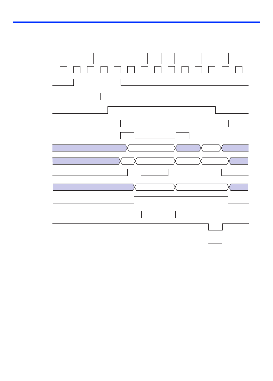
Figure 3. a8237 Timing Waveforms (Part 2 of 3)
Memory-to-Memory DMA Transfer
SI S0 S11 S12 S13 S14 S21 S22 S23 S24 SI
clk
dreq
hrq
hlda
aen
adstb
dbin[7..0]
a8237 Programmable DMA Controller Data Sheet
dbout[7..0]
dben
aout[7..0]
dack
nmemr
nmemw
neopout
A8-A15 Read Data A8-A15 Write Data
Read Address Write Address
Altera Corporation 23
Page 20
a8237 Programmable DMA Controller Data Sheet
Figure 3. a8237 Timing Waveforms (Part 3 of 3)
Host Processor Write Timing
ncs
niowin
ain[3..0]
dbin[7..0]
Host Processor Read Timing
ncs
niorin
ain[3..0]
dbout[7..0]
Variations &
Clarifications
Address Valid
Address Valid
Address Valid
Data Valid
The following list provides clarifications on Altera’s implementation of
the a8237 and the functionality of the Intel 8237A and Harris 82C27A
devices. Altera believes that the a8237 provides consistent functionality
to that of the Intel and Harris devices. These interpretations have been
implemented in the Altera a8237 MegaCore function and are believed to
be consistent with the implementation of the Intel and Harris devices.
■ The neopin is asserted for at least one clock cycle terminates a DMA
cycle at the end of the current transfer. The neopin output is asserted
at the normal conclusion of a DMA cycle, but not asserted when the
DMA cycle is aborted by a neopin.
■ The reset input or the master clear command clears the temporary
data register used in memory-to-memory transfers, including the
temporary address and word count registers.
■ The a8237 does not implement wait-state support for memory-to-
memory transfers.
The following list provides more information on the differences between
Altera’s implementation of the a8237 and the functionality of the Intel
8237A and Harris 82C27A devices.
■ In the a8237 function, tri-state outputs and bidirectional ports are
split into separate inputs, outputs, and enables as necessary.
24 Altera Corporation
Page 21

a8237 Programmable DMA Controller Data Sheet
■ The a8237 does not support the cascade mode because it would not
be an efficient use of device resources. To implement this capability,
the designer should use a hand-coded module or a stripped down
a8237 function.
■ On the rising edge of CLK, the Harris 82C37A deasserts nMEMR on
states 4 and 14, and deasserts nIOROUT on state 4. However, this
approach is not reliable from a timing perspective for a CPLD.
The Altera a8237 deasserts nMEMR on the falling edge of CLK at the
end of states 4 and 14 and nIOROUT at the end of state 4. This action
effectively extends the assertion of these signals by a 1/2 clock cycle.
Revision History
The information contained in the a8237 Programmable DMA Controller Data
Sheet version 1.01 supersedes information published in previous versions.
Version 1.01 includes the following changes:
■ The “State Machine” on page 18 was updated.
■ The waveforms in Figures 2 and 3 were updated.
■ The “Variations & Clarifications” on page 24 was updated.
■ Minor style and text changes were made throughout the document.
Altera Corporation 25
Page 22

Copyright © 1995, 1996, 1997, 1998, 1999 Altera Corporation, 101 Innovation Drive,
San Jose, CA 95134, USA, all rights reserved.
By accessing this information, you agree to be bound by the terms of Altera’s
Legal Notice.
 Loading...