

Page 1
Alpha Industries, Inc. [781] 935-5150 • Fax [617] 824-4579 • Email [email protected] • www.alphaind.com 1
Specifications subject to change without notice. 2/00A
25–31 GHz Amplifier
Features
■ 15 dB Gain
■ +16 dBm Output Power
■ Rugged, Reliable Package
■ Single Voltage Operation
■ 100% RF and DC Testing
AA028P2-99
Description
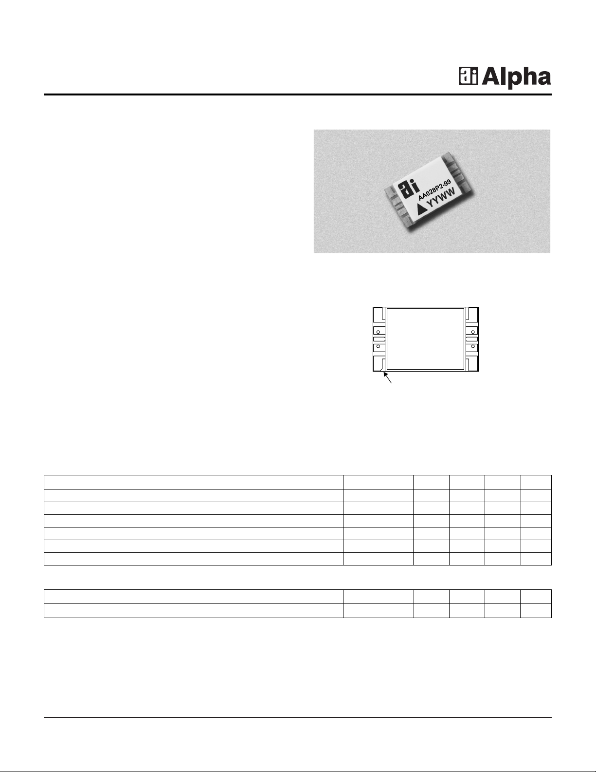
The AA028P2-99 is a broadband millimeterwave amplifier
in a rugged package.The amplifier is designed for use in
millimeterwave communication and sensor systems as a
gain stage in the receiver, transmitter, or local oscillator
chain. The robust ceramic and metal package provides
excellent electrical performance, excellent thermal
performance, and a high degree of environmental
protection for long-term reliability. A single supply voltage
simplifies bias requirements. All amplifiers are screened
at the operating frequencies prior to shipment for
guaranteed performance. Amplifier is targeted for
millimeterwave point-to-point and point-to-multipoint
wireless communications systems.
Parameter Symbol Min. Typ. Max. Unit
Bandwidth BW 25 24—32 31 GHz
Small Signal Gain G12.515 dB
Input Return Loss RL
I
7dB
Output Return Loss RL
O
11 dB
Output Power at 1 dB Gain Compression P
1 dB
14 16 dBm
Temperature Coefficient of Gain dG/dT -0.025 dB/C
Electrical Specifications at 25°C (VD= 5.5 V)
Parameter Symbol Min. Typ. Max. Unit
Drain Current I
D
70 110 mA
DC
RF
Pin Out
N/C
RF In
RF Out
V
D
N/C
PIN 1
INDICATOR
N/C
Page 2
25–31 GHz Amplifier AA028P2-99
2 Alpha Industries, Inc. [781] 935-5150 • Fax [617] 824-4579 • Email [email protected] • www.alphaind.com
Specifications subject to change without notice. 2/00A
Characteristic Value
Operating Temperature (TC) -55°C to +90°C
Storage Temperature (TST) -65°C to +150°C
Bias Voltage (VD1)7 V
DC
Power In (PIN) 13 dBm
Absolute Maximum Ratings
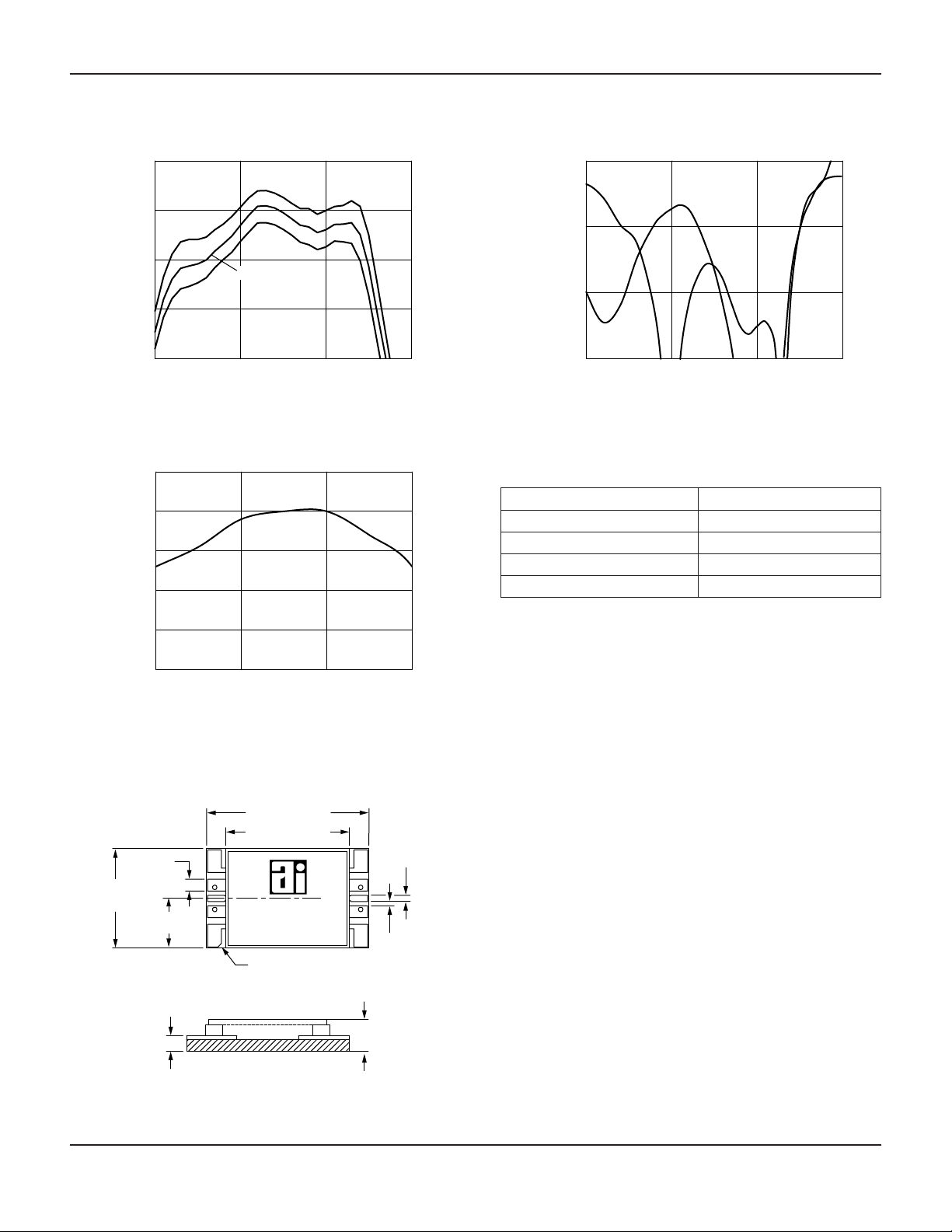
Gain vs. Frequency
20 25 30 35
Frequency (GHz)
Gain (dB)
0
5
10
15
20
-55˚C
+85˚C
+25˚C
Output Power vs. Frequency
Frequency (GHz)
P
1 dB
(dBm)
10
12
14
16
18
20
25 27 29 31
Return Loss vs. Frequency
-15
-10
-5
0
20 25 30 35
Frequency (GHz)
Return Loss (dB)
S
11
S
22
Typical Performance Data
Outline
AA028P2-99
YYWW
0.022
(0.56 mm)
0.180
(4.57 mm)
0.090 (2.29 mm)
0.028
(0.71 mm)
0.057
(1.45 mm)
0.008
(0.20 mm)
0.011
(0.28 mm)
0.295 (7.49 mm)
0.225 (5.72 mm)
PIN 1
IDENTIFICATION
Page 3

25–31 GHz Amplifier AA028P2-99
Alpha Industries, Inc. [781] 935-5150 • Fax [617] 824-4579 • Email [email protected] • www.alphaind.com 3
Specifications subject to change without notice. 2/00A
Typical S-Parameters at 25°C (VD= 5.5 V)
Frequency
S
11
S
21
S
12
S
22
(GHz) Mag. Ang. Mag. Ang. Mag. Ang. Mag. Ang.
16.0 -4.85 152.7 -25.23 -153.3 -63.11 164.5 -1.85 -100.5
18.0 -22.12 70.9 -13.67 123.7 -56.09 3.3 -2.09 -135.0
19.0 -6.24 78.7 -5.74 120.8 -51.64 -45.9 -1.95 -151.8
20.0 -9.94 -19.7 2.66 47.9 -44.79 -43.6 -1.76 -172.1
21.0 -12.26 -100.9 8.02 -27.2 -36.34 -101.1 -2.80 162.8
22.0 -10.95 -129.8 9.36 -103.7 -33.60 178.6 -4.86 147.3
23.0 -7.28 -160.3 9.96 -160.3 -32.63 122.6 -6.35 125.1
24.0 -4.80 167.0 11.61 147.9 -31.12 61.7 -11.42 97.0
24.5 -4.09 148.3 12.40 119.7 -31.48 29.4 -17.03 91.7
25.0 -3.63 130.1 13.50 90.6 -31.62 3.6 -25.61 163.6
25.5 -3.34 109.9 14.51 59.3 -32.27 -18.7 -15.07 -168.1
26.0 -3.68 89.4 15.41 25.1 -31.92 -43.2 -10.85 -179.3
26.5 -4.84 69.8 15.46 -10.0 -32.99 -65.3 -8.85 167.5
27.0 -6.43 50.7 15.24 -44.0 -31.91 -96.7 -7.86 151.6
27.5 -8.29 34.2 14.76 -76.6 -32.44 -112.7 -8.01 136.5
28.0 -10.93 19.1 14.15 -106.7 -31.83 -149.7 -8.98 123.5
28.5 -14.13 7.9 13.49 -132.6 -32.00 -165.7 -10.81 115.6
29.0 -18.80 16.5 13.32 -160.2 -32.53 162.0 -12.53 116.1
29.5 -21.91 37.3 12.75 170.7 -32.92 132.5 -13.15 123.2
30.0 -21.44 46.2 13.03 141.9 -32.84 107.7 -12.56 129.1
30.5 -21.35 23.6 13.57 106.6 -32.41 75.0 -12.21 122.5
31.0 -23.03 -38.4 13.60 70.9 -32.28 41.7 -13.63 114.3
31.5 -15.72 -140.9 13.75 29.7 -30.59 -3.3 -19.81 142.5
32.0 -8.48 167.1 12.55 -19.9 -32.45 -54.3 -9.85 -177.8
32.5 -5.19 127.6 9.33 -73.4 -34.70 -74.9 -5.11 159.1
33.0 -3.37 99.0 4.60 -112.3 -35.29 -100.0 -2.79 140.9
34.0 -1.37 52.2 -6.55 -169.7 -35.54 -139.1 -1.15 101.2
36.0 -1.39 -18.7 -25.55 111.9 -32.62 106.3 6.24 36.6
38.0 -2.82 -77.9 -36.95 34.4 -52.23 66.3 2.80 -49.7
40.0 -4.29 -123.0 -38.71 -98.0 -47.21 147.9 -0.80 -94.1
Page 4

25–31 GHz Amplifier AA028P2-99
4 Alpha Industries, Inc. [781] 935-5150 • Fax [617] 824-4579 • Email [email protected] • www.alphaind.com
Specifications subject to change without notice. 2/00A
Co-Planar Millimeterwave Package
Handling and Mounting
Millimeterwave amplifiers require careful mounting design
to maintain optimal performance.
Handling
The co-planar millimeterwave package is very rugged.
However, due to ceramic’s brittle nature one should
exercise care when handling with metal tools. Do not apply
heavy pressure to the lid. Vacuum tools may be used to
pick and place this part.
Only personnel trained in both ESD precautions and
handling precautions should be allowed to handle these
packages.
Package Construction
The co-planar millimeterwave package is constructed from
metal and ceramic.The base of the package is gold-plated
copper-molybdenum-copper.The lid is unplated alumina.
The lid seal is epoxy.
Mounting Design
The co-planar millimeterwave package is mounted by
placing it in a hole cut in a printed circuit board. The RF
interface on the package should be in the same plane as
the surface of the printed circuit board. The hole should
be cut as close as possible to the outer dimensions of the
package to minimize the gap between package and
printed circuit board. The gap should be no more than
0.005" (0.127 mm). The base of the package should be
mounted directly to a surface which provides a good
ground plane for the printed circuit board and provides a
good thermal ground.
The RF connection on the printed circuit board should
include a microstrip line and two grounded pads, one on
either side of the microstrip line. The RF connection
between the package and the printed circuit board should
be accomplished with three ribbon bonds, one connecting
the RF lines on package and printed circuit board and two
connecting the ground pads on the package and printed
circuit board.
Mounting the Package
The package should be attached to its mounting surface
using a silver-filled conductive paste epoxy. Care should
be taken to ensure that there are no voids or gaps in the
epoxy underfill so that a good ground contact is
maintained.
Connecting the Package
Thermosonic ribbon attachment with 0.00025" x 0.005"
(0.0064 mm x 0.127 mm) gold ribbon is used to make the
connections from the RF and DC package interfaces to
the printed circuit board. Lengths of ribbons should be
minimized.
Ribbon Bonds
Minimize RF
Gap Widths
RF In
Grounded Pad on
Printed Circuit Board
DC Lines
Electrically & Thermally
Conductive Ground Plane
RF Out
Printed Circuit Board
Rogers 4003
0.008" (0.20 mm) Thick
Co-Planar Millimeterwave Package Mounting
 Loading...