

Page 1

ADVANCE INFORMATION
COPYRIGHT © INTEL CORPORATION, 1997 March 1997 Order Number: 272788-002
83C196EA
CHMOS 16-BIT MICROCONTROLLER
Automotive
The 83C196EA is the first member of a new family of microcontrollers with features that are useful in
automotiv e applications, such as powertrain control. Tw o Mbytes of linear address space provide more space
for high-level language compilation. A demultiplexed address/data bus and three chip-select signals make it
easier to design low-cost memory solutions. The external bus can dynamically switch between multiplexed
and demult i pl exed operati on.
NOTE
This datas heet con tai ns in fo rmati on on prod uc ts bein g sampl ed o r in t he i nit ial prod ucti on
phase of development. The specifications are subject to change without notice. Verify
with your loc al Intel sales office that you have the la test datashe et before finalizing a
design.
■ 40 MHz operation
■ Opt ional clock doubler
■ 2 Mbytes of linear address space
■ 1 Kbyte of register RAM
■ 3 Kbytes of code RAM
■ 8 Kbytes of ROM
■ Register-to-register architecture
■ Stack overflow/underflow monitor with
user-defined upper and lower stack
pointer boundary limits
■ 2 peripheral interrupt handlers (PIH)
provide direct ha rdware handling of up
to 16 peripheral interrupts
■ Peripheral transaction server (PTS) with
high-speed, microcoded interrupt
service routines
■ Up to 83 I/O port pins
■ 2 full-duplex serial ports with dedicated
baud-rate generators
■ Enhanced synchronous serial unit
■ 8 pulse-width modulator (PWM) outputs
with 8-bit resolution
■ 16-bit watchdog timer
■ Sixteen 10-bit A/D channels with auto-
scan mode and dedicated results
registers
■ Serial debug unit provides read and
write access to code RAM with no CPU
overhead
■ Chip-select unit (CSU)
■ 3 chip-select pins
■ Dynamic demultip lexed /m ult iple xed
address/data bus for each
chip-select
■ Programmable wait states
(0, 1, 2, or 3) for each chip-select
■ Programmable bus width
(8- or 16-bit) for each chip-select
■ Programmable address range for each
chip-select
■ Event processor array (EPA)
■ 4 flexible 16-bit timer/counters
■ 17 high-speed capture/compare
channels
■ 8 output-only channels capture value of
any other timer upon compare, providing
easy conversio n bet ween an gle and t ime
domains
■ Programmable clock output signal
■ 160-pin QFP package
■ Complete system development support
■ High-speed CHMOS technology
Page 2

Information in this document is provi ded i n connection w ith Intel p r oducts. No license, expres s or implied, by
estoppel or otherwise, to any intellectual property rights is granted by this document. Except as provided in
Intel’s Terms and Conditions of Sale for such products, Intel assumes no liability whatsoever, and Intel disclaims any express or implied warranty, relating to sale and/or use of Intel products including liability or warranties relati ng to fitness for a partic ular purpose, merchan tability, or infringement of any patent, copy right or
other int elle ctua l pr oper ty r ight . I nt el p rodu cts ar e not int en ded fo r use in medic al , l ife sav ing , or li fe sus ta inin g
applicati ons.
Intel retains the right to make changes to specifications and product descriptions at any time, without notice.
*Third-party brands and names are the pr operty of their respective owners.
Copies of documents whi ch have an ordering number and are referenced in this doc ument, or other Intel liter-
ature, may be obtained from:
Intel Corporation
P.O. Box 7641
Mt. Prospec t, IL 60056-7641
or call 1-800-548-4725
Page 3

ADVANCE INFORMATION iii
CONTENTS
83C196EA
CHMOS 16-bit Microcontroller
1.0 Product Overview................................................................................................................ 1
2.0 Nomenclature Overview...................................................................................................... 2
3.0 Pinout.................................................................................................................................. 3
4.0 Signals ................................................................................................................................ 6
5.0 Address Map..................................................................................................................... 15
6.0 Electrical Characteristics........................ ................................. ......... ........ ......... ........ ........ 17
6.1 DC Characteristics........................................................................................................ 17
6.2 AC Characteristics — Multiplexed Bus Mode............................................................... 19
6.3 AC Characteristics — Demultiplexed Bus Mode.......................................................... 23
6.4 Deferred Bus Timing Mode........................................................................................... 27
6.5 AC Characteristics — Serial Port, Shift Register Mode................................................ 28
6.6 AC Characteristics — Synchronous Serial Port ........................................................... 29
6.7 A/D Sample and Conversion Times ............................................................................. 30
6.7.1 AC Characteristics — A/D Converter, 10-bit Mode ...............................................31
6.7.2 AC Characteristics — A/D Converter, 8-bit Mode .................................................32
6.8 External Clock Drive..................................................................................................... 34
6.9 Test Output Waveforms ............................................................................................... 35
7.0 Thermal Characteristics.................................................................................................... 36
8.0 83C196EA Errata.................. ........ ......... ........ ......... ................................. ......... ........ ........ 36
9.0 DataSheet Revision History.............................................................................................. 36
Figures
1. 83C196EA Block Diagram............. ......... ........ ......... ........ .................................. ........ ........ ...1
2. Product Nomenclature .........................................................................................................2
3. 83C196EA 160-pin QFP Package .......................................................................................3
4. System Bus Timing Diagram (Multiplexed Bus Mode).......................................................21
5. READY Timing Diagram (Multiplexed Bus Mode)..............................................................22
6. System Bus Timing Diagram (Demultiplexed Bus Mode) ..................................................25
7. READY Timing Diagram (Demultiplexed Bus Mode).........................................................26
8. Deferred Bus Mode Timing Diagram..................................................................................27
9. Serial Port Waveform — Shift Register Mode....................................................................28
10. Synchronous Serial Port....................................................................................................29
11. External Clock Drive Waveforms........................................................................................34
12. AC Testing Output Waveforms...........................................................................................35
13. Float Waveforms During 5.0 Volt Testing...........................................................................35
Page 4

iv ADVANCE INFORMATION
CONTENTS
Tables
1. Description of Product Nomenclature ..................................................................................2
2. 83C196EA 160-pin QFP Package Pin Assignments............................................................4
3. Pin Assignment Arranged by Functional Categories............................................................5
4. Signal Descriptions ..................... ........ ......... ........ ......... ................................. ......... ........ .....6
5. 83C196EA Address Map....................................................................................................15
6. DC Characteristics at VCC = 4.5 V – 5.5 V..........................................................................17
7. AC Characteristics, Multiplexed Bus Mode........................................................................19
8. AC Timing Symbol Definitions............................................................................................20
9. AC Characteristics, Demultiplexed Bus Mode ...................................................................23
10. Serial Port Timing — Shift Register Mode .........................................................................28
11. Synchronous Serial Port Timing......................................................................................... 29
12. 10-bit A/D Operating Conditions (1)...................................................................................31
13. 10-bit Mode A/D Characteristics Over Specified Operating Conditions (7)........................31
14. 8-bit A/D Operating Conditions (1).....................................................................................32
15. 8-bit Mode A/D Characteristics Over Specified Operating Conditions (7)..........................33
16. External Clock Drive...........................................................................................................34
Page 5
ADVANCE INFORMATION 1
83C196EA CHMOS 16-BIT MICROCONTROLLER — AUTOMOTIVE
1.0 PRODUCT OVERVIEW
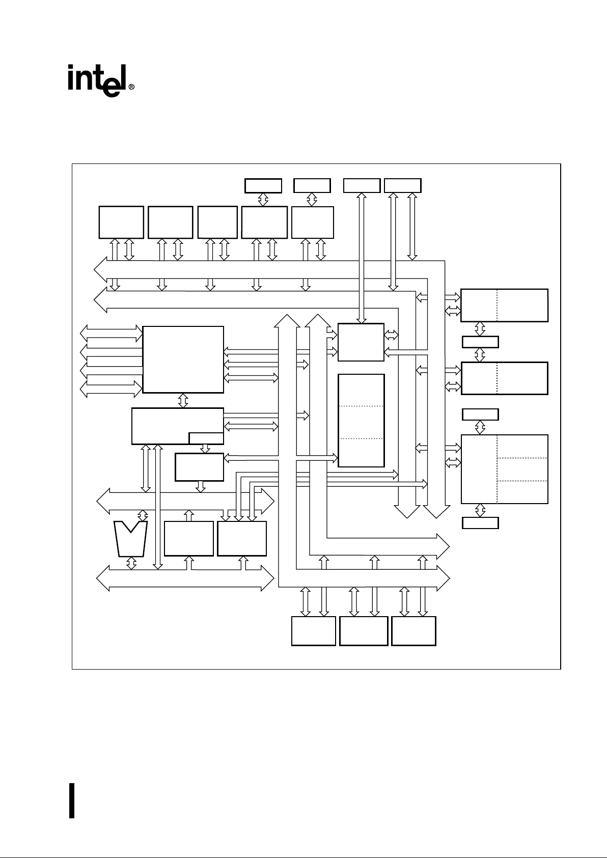
Figure 1. 83C 196EA Block Diagram
The 83C196EA is highly integrated with an enhanced peripheral set. The serial debug unit (SDU) provides
system debug and development capabi lities. The SDU can set a single hardware breakpoint and provides
read and write access to code RAM through a high-speed, dedicated serial link. A stack overflow/underflow
monitor assists in code development by causing an unmaskable interrupt if the stack pointer crosses a userdefined boundary. The 16-channel A/D converter supports an auto-scan mode that operates with no CPU
Code/Data
RAM
3 Kbytes
EPORT
Queue
A20:16
Source (16)
Destination (16)
AD15:0
SIO0
Baud-rate
Generator
EPA 4 Timers
Ports 7,8
Port 11
17 Capture/
Compares
A/D
Converter
Bus
Controller
A15:0
Serial Debug
Unit
Watchdog
Timer
Stack
Overflow
Module
Pulse-width
Modulators
SSIO0
SSIO1
ROM
8 Kbytes
A3178-03
SIO1
Baud-rate
Generator
Port 10
Bus-Control
Interface Unit
Microcode
Engine
Chip-select
Unit
Peripheral
Transaction
Server
Memory
Interface
Unit
Register
RAM
1 Kbyte
ALU
Interrupt
Controller
Peripheral
Interrupt
Handler
Bus Control
Peripheral Addr Bus (10)
Peripheral Data Bus (16)
Memory Addr Bus (24)
Port 12
8 Output/
Simulcaptures
Port 9
Port 2
Memory Data Bus (16)
Page 6
2 ADVANCE INFORMATION
83C196EA CHMOS 16-BIT MICROCONTROLLER — AUTOMOTIVE
overhead. Each A/D channel has a dedicated result register. The EPA supports high-speed input captures
and output compares with 17 programmable, high-speed capture/compare channels. Eight output-only
channels provide support for time-base conversions by capturing the value of one of four timers when a
comp a r e oc curs.
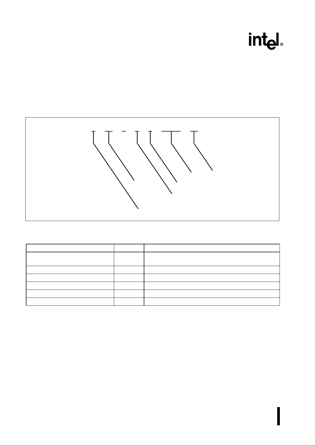
2.0 NOMENCLATURE OVERVIEW
Figure 2. Product Nomenclature
Table 1. Description of Product Nomenclature
Parameter Options Description
Temperature and Burn-in Opti ons A Automotive operating temperature range (–40° C to
125° C case) with Intel standa rd burn-in.
Packaging Options S QFP
Program Memory Options 3 Internal ROM
Process Information C CHMOS
Product Family 196EA
Device Speed no mark 40 MHz
Program Memory Options
XXXXX XXXX8XXX
Packaging Options
Temperature and Burn-in Options
A2815-01
Process Information
Product Family
Device Speed
Page 7
ADVANCE INFORMATION 3
83C196EA CHMOS 16-BIT MICROCONTROLLER — AUTOMOTIVE
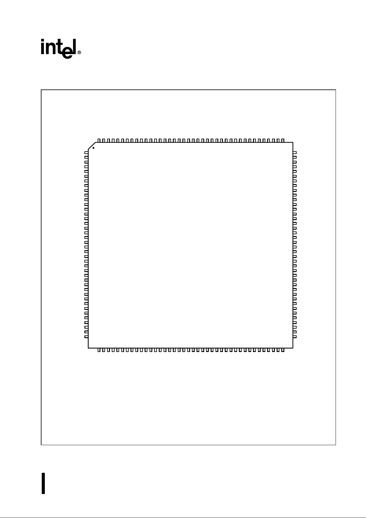
3.0 PINOUT
Figure 3. 83C196EA 160-pin QFP Package
A3151-02
120
119
118
117
116
115
114
113
112
111
110
109
108
107
106
105
104
103
102
101
100
99
98
97
96
95
94
93
92
91
90
89
88
87
86
85
84
83
82
81
AS83C196EA
View of component as
mounted on PC board
1
2
3
4
5
6
7
8
9
10
11
12
13
14
15
16
17
18
19
20
21
22
23
24
25
26
27
28
29
30
31
32
33
34
35
36
37
38
39
40
41
42
43
44
45
46
47
48
49
50
51
52
53
54
55
56
57
58
59
60
61
62
63
64
65
66
67
68
69
70
71
72
73
74
75
76
77
78
79
80
160
159
158
157
156
155
154
153
152
151
150
149
148
147
146
145
144
143
142
141
140
139
138
137
136
135
134
133
132
131
130
129
128
127
126
125
124
123
122
121
AD0 / P3.0
AD1 / P3.1
AD2 / P3.2
AD3 / P3.3
AD4 / P3.4
AD5 / P3.5
AD6 / P3.6
AD7 / P3.7
V
CC
V
CC
V
SS
V
SS
AD8 / P4.0
AD9 / P4.1
AD10 / P4.2
AD11 / P4.3
AD12 / P4.4
AD13 / P4.5
AD14 / P4.6
AD15 / P4.7
P5.7 / RPD
P5.4/BREQ#/TMODE#
P5.6 / READY
P5.1 / INST
P5.0 / ALE
P5.5 / BHE# / WRH#
P5.3 / RD#
P5.2 / WR# / WRL#
V
SS
V
CC
A20 / EPORT.4
A16 / EPORT.0
A17 / EPORT.1
A18 / EPORT.2
A19 / EPORT.3
EPORT.5 / CS0#
EPORT.6 / CS1#
EPORT.7 / CS2#
NC
NC
NC
NC
NC
NC
EA#
V
CC
PLLEN
XTAL2
XTAL1
V
SS
V
CC
P2.7 / CLKOUT
P2.6 / ONCE#
P2.5
P2.4 /RXD1
P2.3 / TXD1
P2.2 / EXTINT
P2.1 / RXD0
P2.0 / TXD0
V
CC
V
SS
CRBUSY#
CROUT
CRIN
CRDCLK
V
CC
NC
V
SS
V
SS
ACH15
ACH14
ACH13
ACH12
ACH11
ACH10
ACH9
ACH8
ACH7
ACH6
NC
A15
A14
A13
A12
A11
A10
A9
A8
V
CC
V
SS
A7
A6
A5
A4
A3
A2
A1
A0
P9.7 / OS7
P9.6 / OS6
P9.5 / OS5
P9.4 / OS4
P9.3 / OS3
P9.2 / OS2
P9.1 / OS1
P9.0 / OS0
P7.0 / EPA0 / T1CLK
P7.1 / EPA1 / T1RST
P7.2 / EPA2 / T2CLK
P7.3 / EPA3 / T2RST
P7.4 / EPA4 / T3CLK
P7.5 / EPA5 / T3RST
V
SS
V
CC
P7.6 / EPA6 / T4CLK
P7.7 / EPA7 / T4RST
P8.7 / EPA15
P8.6 / EPA14
P8.5 / EPA13
NC
P8.4 / EPA12
P8.3 / EPA11
P8.2 / EPA10
P8.1 / EPA9
P8.0 / EPA8
P10.5
P10.4 / EPA16
P10.3 / SD1
P10.2 / SC1 / CHS#
P10.1 / SD0
P10.0 / SC0
P11.4 / PWM4
P11.5 / PWM5
P11.6 / PWM6
P11.7 / PWM7
P11.3 / PWM3
P11.2 / PWM2
P11.1 / PWM1
P11.0 / PWM0
V
SS
V
CC
P12.4
P12.0
P12.1
P12.2
P12.3
V
SS
NC
V
CC
NC
RESET#
NMI
V
REF
ANGND
ACH0
ACH1
ACH2
ACH3
ACH4
ACH5
†
††
This pin supplies voltage to the phase-locked loop circuitry, so use extra care to keep it stable.
This pin supplies voltage to the code RAM. Maintain at 5 volts to retain data in code RAM.
NC pins must be unconnected to prevent accidental entry into a test mode.
†††
Page 8
4 ADVANCE INFORMATION
83C196EA CHMOS 16-BIT MICROCONTROLLER — AUTOMOTIVE
Table 2. 83C196EA 160-pin QF P Package Pin Assi gnments
Pin Name Pin Name Pin Name Pin Name
1 AD0 / P3.0 41 NC 81 ACH5 121 NC
2 AD1 / P3.1 42 NC 82 ACH4 122 P8.5 / EPA13
3 AD2 / P3.2 43 NC 83 ACH3 123 P8.6 / EPA14
4 AD3 / P3.3 44 NC 84 ACH2 124 P8.7 / EPA15
5 AD4 / P3.4 45 EA# 85 ACH1 125 P7.7 / EPA7 / T4RST
6 AD5 / P3.5 46 V
CC
86 ACH0 126 P7.6 / EPA6 / T4CLK
7 AD6 / P3.6 47 PLLEN 87 ANGND 127 V
CC
8 AD7 / P3.7 48 XTAL2 88 V
REF
128 V
SS
9V
CC
49 XTAL1 89 NMI 129 P7.5 / EPA5 / T3RST
10 V
CC
50 V
SS
90 RESET# 130 P7.4 / EPA4 / T3CLK
11 V
SS
51 V
CC
91 NC 131 P7.3 / EPA3 / T2RST
12 V
SS
52 P2.7 / CLKOUT 92 V
CC
132 P7.2 / EPA2 / T2CLK
13 AD8 / P4.0 53 P2.6 / ONCE# 93 NC 133 P7.1 / EPA1 / T1RST
14 AD9 / P4. 1 54 P2.5 94 V
SS
134 P7.0 / EPA0 / T1CLK
15 AD10 / P4.2 55 P2.4 / RXD1 95 P12.3 135 P9.0 / OS0
16 AD11 / P4.3 56 P2.3 / TXD1 96 P12.2 136 P9.1 / OS1
17 AD12 / P4.4 57 P2.2 / EXTINT 97 P12.1 137 P9.2 / OS2
18 AD13 / P4.5 58 P2.1 / RXD0 98 P12.0 138 P9.3 / OS3
19 AD14 / P4.6 59 P2.0 / TXD0 99 P12.4 139 P9.4 / OS4
20 AD15 / P4.7 60 V
CC
100 V
CC
140 P9. 5 / OS5
21 P5.7 / RPD 61 V
SS
101 V
SS
141 P9. 6 / OS6
22 P5.4/BREQ#/TMODE# 62 CRBUSY# 102 P11.0 / PWM0 142 P9.7 / OS7
23 P5.6 / READY 63 CROUT 103 P11.1 / PWM1 143 A0
24 P5.1 / INST 64 CRIN 104 P11.2 / PWM2 144 A1
25 P5.0 / ALE 65 CRDCL K 105 P11.3 / PWM3 145 A2
26 P5.5 / BHE# / WRH# 66 V
CC
106 P11.7 / PWM7 146 A3
27 P5.3 / RD # 67 NC 107 P11.6 / PWM6 147 A4
28 P5.2 / WR# / WRL# 68 V
SS
108 P11.5 / PWM5 148 A5
29 V
SS
69 V
SS
109 P11.4 / PWM4 149 A6
30 V
CC
70 ACH15 110 P10.0 / SC0 150 A7
31 A20 / EPORT.4 71 ACH14 111 P10.1 / SD0 151 V
SS
32 A16 / EPORT.0 72 ACH13 112 P10.2 / SC1 152 V
CC
33 A17 / EPORT.1 73 ACH12 113 P10.3 / SD1 153 A8
34 A18 / EPORT.2 74 ACH11 114 P10.4 / EPA16 154 A9
35 A19 / EPORT.3 75 ACH10 115 P10.5 155 A10
36 EPORT.5 / CS0# 76 ACH9 116 P8.0 / EPA8 156 A11
37 EPORT.6 / CS1# 77 ACH8 117 P8.1 / EPA9 157 A12
38 EPORT.7 / CS2# 78 ACH7 118 P8.2 / EPA10 158 A13
39 NC 79 ACH6 119 P8.3 / EPA11 159 A14
40 NC 80 NC 120 P8.4 /EPA12 160 A15
Page 9
ADVANCE INFORMATION 5
83C196EA CHMOS 16-BIT MICROCONTROLLER — AUTOMOTIVE
Table 3. Pin Assignment Arranged by Functional Categories
Addr & Data Input/Output Input/Output (Cont’d) Input/Output (Cont’d)
Name Pin Name Pin Name Pin Name Pin
A0 143 P2.0 / TXD0 59
EPORT.7 38 P12.0 98
A1 144 P2.1 / RXD0 58
P7.0 / EPA0 / T1CLK 134 P12.1 97
A2 145 P2.2 57
P7.1 / EPA1 / T1RST 133 P12.2 96
A3 146 P2.3 / TXD1 56
P7.2 / EPA2 / T2CLK 132 P12.3 95
A4 147 P2.4 / RXD1 55
P7.3 / EPA3 / T2RST 131 P12.4 99
A5 148 P2.5 54
P7.4 / EPA4 / T3CLK 130
A6 149 P2.6 53 P7.5 / EPA5 / T3RST 129 Analog Inputs
A7 150 P2.7 52
P7.6 / EPA6 / T4CLK 126 Name Pin
A8 153 P3.0 1
P7.7 / EPA7 / T4RST 125 ACH0 86
A9 154
P3.1 2 P8.0 / EPA8 116 ACH1 85
A10 155 R3.2 3
P8.1 / EPA9 117 ACH2 84
A11 156 P3.3 4
P8.2 / EPA10 118 ACH3 83
A12 157
P3.4 5 P8.3 / EPA11 119 ACH4 82
A13 158 P3.5 6
P8.4 / EPA12 120 ACH5 81
A14 159 P3.6 7
P8.5 / EPA13 122 ACH6 79
A15 160 P3.7 8
P8.6 / EPA14 123 ACH7 78
A16 32 P4.0 13
P8.7 / EPA15 124 ACH8 77
A17 33 P4.1 14
P9.0 / OS0 135 ACH9 76
A18 34 P4.2 15
P9.1 / OS1 136 ACH10 75
A19 35 P4.3 16
P9.2 / OS2 137 ACH11 74
A20 31 P4.4 17
P9.3 / OS3 138 ACH12 73
AD0 1
P4.5 18 P9.4 / OS4 139 ACH13 72
AD1 2 P4.6 19
P9.5 / OS5 140 ACH14 71
AD2 3 P4.7 20
P9.6 / OS6 141 ACH15 70
AD3 4
P5.0 25 P9.7 / OS7 142
AD4 5 P5.1 24
P10.0 / SC0 110 Bus Control & Status
AD5 6 P5.2 28
P10.1 / SD0 111 Name Pin
AD6 7 P5.3 27
P10.2 / SC1 112 ALE 25
AD7 8 P5.4 22
P10.3 / SD1 113 BHE#/WRH# 26
AD8 13 P5.5 26
P10.4 / EPA16 114 BREQ# 22
AD9 14 P5.6 23
P10.5 115 CS0# 36
AD10 15
P5.7 21 P11.0 / PWM0 102 CS1# 37
AD11 16
EPORT.0 32 P11.1 / PWM1 103 CS2# 38
AD12 17
EPORT.1 33 P11.2 / PWM2 104 INST 24
AD13 18
EPORT.2 34 P11.3 / PWM3 105 RD# 27
AD14 19
EPORT.3 35 P11.4 / PWM4 109 READY 23
AD15 20
EPORT.4 31 P11.5 / PWM5 108
EPORT.5 36 P11.6 / PWM6 107
EPORT.6 37 P11.7 / PWM7 106 WR#/WRL# 28
Page 10
6 ADVANCE INFORMATION
83C196EA CHMOS 16-BIT MICROCONTROLLER — AUTOMOTIVE
4.0 SIGNALS
Power & Ground Processor Control
Name
Pins Name Pin
ANGND
87 CLKOUT 52
V
CC
9, 10, 30, 46†, 51, 60, 66††, 92, 100, 127, 152 EA# 45
V
SS
11, 12, 29, 50, 61, 68, 69, 94, 101, 128, 151 EXTINT 57
V
REF
88 NMI 89
ONCE# 53
No Connection PLLEN 47
Name
Pins RESET# 90
NC
†††
39–44, 67, 69, 80, 91, 93, 121 RPD 21
TMODE# 22
XTAL1 49
XTAL2 48
†
This pin sup pl ies voltage to the phase-locked loop circuitry, so use extra
care to keep it stable.
††
This pin supplies voltage to code RAM. To retain data, maintain 5 volts.
†††
Always leave NC (no connect) pins unconnected to prevent accidental
entry into test modes.
Code Debug
Name Pin
CRBUSY# 62
CRDCLK 6 5
CRIN 64
CROUT 63
Table 4. Signal Descriptions
Name Type Description
A15:0 I/O System Address Bus
These address lines provide address bits 0–15 during the entire external
memory cycle during both multiplexe d and demultiplex ed bus modes.
A20:16 I/O Address Li nes 16–20
These address lines provide address bits 16–20 during the entire external
memory cycle, supporting extended addressing of the 2 Mbyte address space.
NOTE: Internally, there are 24 address bits; however, only 21 external
address pins (A20:0) are implemented. The internal address space is
16 Mbytes (000000–FFFFFFH) and the external addr ess space is 2
Mbytes (00000–1FFFFFH). The device resets to FF2080H in internal
memory or 1F2080H in external memory.
A20:16 are multiplexed with EPORT.4:0.
ACH15:0 I Analog Channels
These pins are analog inputs to the A/D converter.
The ANGND and V
REF
pins must be con nected for the A/D converter to functi on.
Table 3. Pin Assignment Arranged by Functional Categories (Continued)
Page 11

ADVANCE INFORMATION 7
83C196EA CHMOS 16-BIT MICROCONTROLLER — AUTOMOTIVE
AD15:0 I/O Address/Data Lines
The function of these pins depend on the bus size and mode. When a bus
access is not occurring, these pins revert to their I/O port function.
16-bit Multiplexed Bus Mode:
AD15:0 dr ive ad dres s bit s 0– 15 d uring th e firs t half of t he bus cycl e and driv e or
receive dat a during the second half of the bus cycle.
8-bit Multiplexed Bus Mode:
AD15:8 drive address bits 8–15 during the ent i re bus cycle. AD7:0 drive
address bit s 0–7 during the first half of the bus cycle and drive or r eceive data
during the second half of the bus cycle .
16-bit D em u lt ip lexed Mode :
AD15:0 drive or receive data during the entire bus cycle.
8-bit Demultiplexed Mode:
AD7:0 drive or receive data dur ing the en tire bus cycle. AD1 5 :8 driv e the data
that is cur r ently on the high byte of the internal bus.
ALE O Address Latch Enable
This active-high output signal is asserted only during external memory cycles.
ALE signals the start of an external bus cycle and indicates that valid address
information is available on the system address/da ta bus (A20:16 and AD1 5:0
for a multipl exed bus; A20:0 for a de mul tiplexed bus).
An external latch can use thi s signal to demul tiplex address bits 0–15 from the
address/data bus in multiplexed mode.
ALE shares a package pin with P5.0.
ANGND GND Analog Ground
ANGND must be connected for A/D converter operat i on. ANGND and V
SS
should be nomi nally at the same potential.
BHE# O Byte High Enable
†
During 16-bi t bus cycles, this active-low output signal is asserted for w ord and
high-byte reads and wri tes to external memory. BHE# indicates that valid data
is being transferred over the upper half of the system data bus. Use BHE#, in
conjunct i on with AD0, to determine which memory byte is being transferred
over the system bus:
BHE# AD0 Byte(s) Accessed
0 0 both bytes
0 1 high byte only
1 0 low byte only
BHE# shares a package pin with P5.5 and WRH#.
†
The chip configuration register 0 (CCR0) determines whether this pin functions as BHE# or WRH#. CCR0.2 = 1 selects BHE#; CCR0.2 = 0 selects
WRH#.
BREQ# O Bus Request
This active-low output signal is assert ed during a hold cycl e w hen the bus
controller has a pending external memory cycle.
You must enable the bus-ho l d protocol before using this signal.
BREQ# shares a package pin with P5.4.
Table 4. Signal Descriptions (Continued)
Name Type Description
Page 12
8 ADVANCE INFORMATION
83C196EA CHMOS 16-BIT MICROCONTROLLER — AUTOMOTIVE
CLKOUT O Clock Output
Output of the internal clo ck generator. The CLKOUT frequency can be
programmed to one of five frequencies: the internal operating frequency (f)
divided by a factor of two, four, eight, or sixteen, or the s ame frequency as the
oscillator input (F
XTAL1
). CLKOUT has a 50% d uty cycle.
CLKOUT shares a package pin with P2.7
CRBUSY# O Code RAM Busy
This signal indicates that the serial debug unit (SDU) is not ready to conduct a
transaction.
CRDCLK I Code RAM Clock
Provides the clock signal for the serial debug unit (SDU). The maxi mum clock
frequency equals the operati ng frequency (f) divided by two.
CRIN I Code RAM Data Input
Serial input for test instructions and dat a i nto the serial debug unit (SDU). Da ta
is transfer red in 8-bit byte s wit h the mos t-s ignif ican t bit (MSB ) fir st. Each by te i s
sampled on the rising edge of CRDCLK.
CROUT O Code RAM Data Output
Serial output for data from the serial debug unit (SDU). Data is transferred in 8bit bytes with the most-signif i cant bit (MSB) first. Each byt e is valid on the ri sing
edge of CRDCLK.
CS2:0# O Chip-select Lines 0–2
The active-low output CS
x
# is asserted during an external memory cycle when
the address to be accessed is in the range programme d for chip select
x
. If the
external memory address is outs ide the range assigned to the three chip
selects, no chip-select output is ass e rted and the bus configuration defaults to
the CS2# values.
Immediately following res et, CS0# is automatically assi gned to the range
FF2000–FF20FFH (1F2000–1F20FFH if external).
CS2:0# share package pins with EPORT.7:5.
EA# I External Ac ce s s
This input determines whether memory accesses to special -purpose and
program memory partitions (FF2000–FF3FFFH) are directed to internal or
external memory. These accesses are directed to internal memory if EA# is
held high and to extern al memo ry if EA# is he ld low . For an ac ces s to any ot her
memory location, the value of EA# is irrelevant.
EA# is sampled and latched only on the rising edge of RESET#. Changing the
level of EA# aft er reset has no effect.
On devices with no internal nonvolatile memory, always c onnect EA# to V
SS
.
EPA16:0 I/O Event Proc essor Array (EPA) Capture/Compare Channels
High-speed input/output signals for the EPA capture/compare channels.
EPA16:0 share package pins with the followi ng signals : EPA0/P7.0/T 1CLK,
EPA1/P7.1/T1RST, EPA2/P7.2/T2CLK, EPA3/P7.3 /T 2RST,
EPA4/P7.4/T3CLK, EPA5/P7.5/T3RST, EPA6/P7.6/T4CLK,
EPA7/P7.7/T4RST, EPA 8 /P8.0, EPA9/P8.1, EPA10/P8.2, EPA11/P8.3,
EPA12/P8.4, EPA13/P8.5, EPA14/P8.6, EPA 15/P8.7, and EPA16/P10.4.
Table 4. Signal Descriptions (Continued)
Name Type Description
Page 13

ADVANCE INFORMATION 9
83C196EA CHMOS 16-BIT MICROCONTROLLER — AUTOMOTIVE
EPORT.7:0 I/O Extended Addressing Port
This is a standard 8-bit, bi di rectional port.
EPORT.4:0 share package pins with A20:16. EPORT7:5 share package pins
with CS2:0#.
EXTINT I External Interru pt
In normal operating mode, a ri sing edge on EXTINT sets the EXTINT i nterrupt
pending bit . EXTINT is sampled during phase 2 (CLKOUT hig h). The minimum
high time is one state time.
In powerdown mode, asserting the EX TINT signal for at least 50 ns causes the
device to resume normal operation. The interrupt need not be enabled, but the
pin must be con figured as a special-function input. If the EXTINT interrupt is
enabled, the CPU executes the interrupt service routine. Otherwise, the CPU
executes the i nst ruct ion tha t imme diat el y foll ow s th e comman d t hat i nvoked th e
power-saving mode.
In idle mode, asserting any enabled interrupt causes the device to resu me
normal opera tion.
EXTINT shares a package pin with P2.2.
INST O Instruction Fetch
This active-high output signal is valid only during external memory bus cycl es.
When high, INST indicates that an instruction is being fetched from external
memory. The signal remains high during the enti re bus cycle of an external
instruction fetch. INST is low for data accesses, including interrupt vector
fetches and chip configuration byte reads. INST is low during internal memory
fetches.
INST shares a package pin with P5.1.
NMI I Nonmaskable Interrupt
In normal operating mode, a rising edge on NMI generates a nonmaskable
interrupt. NMI has the highest priority of all prioritized interrupts. Assert NMI for
greater than one state time to guarantee that it is recognized.
ONCE# I On-circuit Emulation
Holding ONCE# low during the ris i ng edge of RESET# places the device into
on-circuit emulation (ONCE) mode. This mode pu ts all pins into a highimpedance state, thereb y isolating th e device from other components in t he
system. The value of ONCE# is latched when the RESET# pin goes inactive.
While the device is in ONCE mode, you can debug the system using a clip-on
emulator.
To exit ONCE mode, reset the device by pulling the RESET# signal low. To
prevent inadvertent ent ry into ONCE mode, either configure this pin as an
output or hol d it high durin g reset and ensure that your system meets the V
IH
specification.
ONCE# shares a package pin with P2.6.
OS7:0 O E vent Processor Array (EPA) Compare-only Channels with Simulcapt ure
Outputs of the EPA’s compare- only channels. These pins are multiplexed with
port 9 and may be configured as standard I/O.
OS7:0 share package pins with P9.7:0.
Table 4. Signal Descriptions (Continued)
Name Type Description
Page 14

10 ADVANCE INFORMATION
83C196EA CHMOS 16-BIT MICROCONTROLLER — AUTOMOTIVE
P2.7:0 I/O Port 2
This is a standard, 8-bit, bi di rectional port that is multiplexed with individually
selectable special-function signals. P2.6 is multiplexed with ONCE#. To prevent
inadvertent e ntry int o ONCE mode, eit he r con fig ure thi s p in a s an ou tp ut or ho ld
it high during res et and ensure that your system meets the V
IH
specification.
Port 2 shares pack age pins with the following signals: P2.0/TXD0, P2.1/RXD0,
P2.2/EXTINT, P2.3/TXD1, P2.4/RXD1, P2.6/ONCE#, and P2.7/CLKOUT.
P3.7:0 I/O Port 3
This is a memory-mapped, 8-bit, bidi rectional port w i th programmable op endrain or complementary output modes. T he pins are shared with the
multiplexed address/data bus, which has complementary drivers.
P3.7:0 share package pins with AD7:0.
P4.7:0 I/O Port 4
This is a memory-mapped, 8-bit, bidi rectional port w i th programmable op endrain or complementary output modes. T he pins are shared with the
multiplexed address/data bus, which has complementary drivers.
P4.7:0 share package pins with AD15:8.
P5.7:0 I/O Port 5
This is a memory- mapped, 8-bit, bidirectional port that is multi plexed with
individual ly selectable control si gnals. P5.4 i s multiplexed wi th TMODE#. If this
pin is held low during reset, the dev ice will enter a test mode. To prevent
inadvertent entry into a reserved test mode, either configure this pin as an
output or hold i t high during reset and ensure that your system meets th e V
IH
specification.
Port 5 shares pack age pins with the following signals: P5.0/ALE, P5.1/INST,
P5.2/WR#/WRL#, P5.3/RD#, P5.4/BREQ#/TMODE#, P5.5/BHE#/WRH#,
P5.6/READY, and P5.7/RPD.
P7.7:0 I/O Port 7
This is a standard, 8-bit, bi di rectional port that is multiplexed with individually
selectable special-function signals.
Port 7 shares pack age pins with the following signals: P7.0/EPA0/T 1CLK,
P7.1/E PA1/T1RS T , P7 .2 /E PA2/T2CL K, P7.3/EPA3/ T 2 R ST,
P7.4/EPA4/T3CLK, P7.5/EPA5/T3RST, P7.6/EPA6/T4CLK, and
P7.7/EPA7/T4RST.
P8.7:0 I/O Port 8
This is a standard, 8-bit, bi di rectional port that is multiplexed with individually
selectable special-function signals.
P8.7:0 share package pins with EPA15:8.
P9.7:0 I/O Port 9
This is a standard, 8-bit, bi di rectional port that is multiplexed with individually
selectable special-function signals.
P9.7:0 share package pins with OS 7:0.
Table 4. Signal Descriptions (Continued)
Name Type Description
Page 15

ADVANCE INFORMATION 11
83C196EA CHMOS 16-BIT MICROCONTROLLER — AUTOMOTIVE
P10.5:0 I/O Port 10
This is a standard, 6-bit, bidirectional port that is mult i plexed with individually
selectable special - function signals.
Port 10 shar es pac kage pins w ith the fo ll owin g si gnal s: P10 .0/S C0, P10.1/ SD0 ,
P10.2/SC1, P10.3/SD 1, P10.4/EPA16, and P10.5.
P11.7:0 I/O Port 11
This is a standard, 8-bit, bidirectional port that is mult i plexed with individually
selectable special - function signals.
P11.7:0 s hare package pins with PWM7:0.
P12.4:0 I/O Port 12
This is a memory-ma ppe d, 5-bi t, bid irect iona l por t. P1 2.2: 0 sel ect the t est -ROM
execution mode.
PLLEN I Phase-l ocked Loop Enable
This active-high input pi n enables the on-chip clock doubler.
PWM7:0 O Pulse Width Modulator Outputs
These are PWM output pins with high-current drive capability.
PWM7:0 share pa ckage pins with P11.7:0.
RD# O Read
Read-signal output to external memory. RD# is asserted only during ext ernal
memory reads.
RD# shares a package pin with P5.3.
READY I Ready Input
This active-high input signal is used to lengthen external memory cycles for
slow memory by ge nerating wait st ates in addition to the wait sta tes that are
generated i nternally.
When READY is high, CPU operation continues in a normal manner with wait
states inserted as programme d i n the chip configuration registers or the chipselect
x
bus control register. READY is ignored for all internal memory
accesses.
READY shares a package pin with P5.6.
RESET# I/O Reset
A level-sensitive rese t i nput to and open-drain system reset output from the
microcontroller. Either a falling edge on RESET# or an internal reset turns on a
pull-d ow n transistor connected to t he R ESET# pin for 16 state times. In the
powerdown and idle modes, asserting RESET# causes the chip to reset and
return to normal operati ng mode. After a device reset, the first instruction fetch
is from FF2080H (or 1F2080H in external memory).
Table 4. Signal Descriptions (Continued)
Name Type Description
Page 16

12 ADVANCE INFORMATION
83C196EA CHMOS 16-BIT MICROCONTROLLER — AUTOMOTIVE
RPD I Return from Powerdown
Timing pin for the return-from-pow erdown circuit.
If your application uses powerdown mode, connect a capacitor be tween RPD
and V
SS
if either of the following conditions are true.
• the internal oscillator is the clock source
• the phase-locked loop (PLL) circuitr y is enabled (see PLLEN signal
description)
The capacitor causes a delay that enables the oscillator and PLL circuitry to
stabilize before the internal CPU and peripheral clocks are enabled.
The capacitor is not required if your applicati on uses powerdown mode and if
both of the following conditio ns are true.
• an external clock input is the clock source
• the phase-locked loop circ uitry is disabl ed
If your application does not use powerdown mode, leave this pin unconnected.
RPD shares a package pin with P5.7.
RXD1:0 I/O Receive Serial Data 0 and 1
In modes 1, 2, and 3, RXD0 and 1 receive s erial port inpu t data. In mode 0, they
functions as either inputs or open-drain outputs for data.
RXD0 shares a package pin with P2.1 and RXD1 shares a package pin with
P2.4.
SC1:0 I/O Clock Pins for SSI O0 and 1
For handshaking mode, configure SC1:0 as open-drain outputs.
This pin carries a signal only during receptions and transmissi ons. When the
SSIO port is idle , the pi n remain s eithe r high (wi th hands h aking) or low (with out
handshaking ).
SC0 shares a package pin with P1 0.0, and SC1 shares a package pin with
P10.2.
SD1:0 I/O Data Pins for SSIO0 and 1
These pins are the data I/O pins for SSIO0 and 1.
SD0 shares a package pin with P1 0.1, and SD1 shares a package pin with
P10.1.
T1CLK I Timer 1 External Clock
External cloc k for timer 1.Timer 1 is programmable to increment or dec ement
on the rising edge, the falling edge, or both rising and falling edges of T1CLK.
and
External cloc k for the serial I/O baud-rate generator input (program selectable).
T1CLK shares a package pin with P7.0 and EPA0.
T2CLK I Timer 2 External Clock
External clock for timer 2. Timer 2 is programmable to increment or decement
on the rising edge, the falling edge, or both rising and falling edges of T2CLK.
T2CLK shares a package pin with P7.2 and EPA2.
Table 4. Signal Descriptions (Continued)
Name Type Description
Page 17

ADVANCE INFORMATION 13
83C196EA CHMOS 16-BIT MICROCONTROLLER — AUTOMOTIVE
T3CLK I Timer 3 External Clock
External c lock for timer 3. T i mer 3 i s programmable to increment or decement
on the rising edge, the falling edge, or both rising and falling edges of T3CLK.
T3CLK share s a package pin with P7.4 and EPA4.
T4CLK I Timer 4 External Clock
External c lock for timer 4. T i mer 2 i s programmable to increment or decement
on the rising edge, the falling edge, or both rising and falling edges of T4CLK.
T4CLK share s a package pin with P7.6 and EPA6.
T1RST I Timer 1 External Reset
External res et for timer 1. Timer 1 is programmable to reset on the risi ng edge,
the falling edge, or both rising and falling edges of T1RST.
T1RST shar es a package pin wi th P7.1 and EPA1 .
T2RST I Timer 2 External Reset
External res et for timer 2. Timer 2 is programmable to reset on the risi ng edge,
the falling edge, or both rising and falling edges of T2RST.
T2RST shar es a package pin wi th P7.3 and EPA3 .
T3RST I Timer 3 External Reset
External res et for timer 3. Timer 3 is programmable to reset on the risi ng edge,
the falling edge, or both rising and falling edges of T3RST.
T3RST shar es a package pin wi th P7.5 and EPA5 .
T4RST I Timer 4 External Reset
External res et for timer 4. Timer 4 is programmable to reset on the risi ng edge,
the falling edge, or both rising and falling edges of T4RST.
T4RST shar es a package pin wi th P7.6 and EPA6 .
TMODE# I Test-Mode Entry
If this pin is held low during reset, the de vice will enter a test mode. The value of
several other pins defines the actual test mode. All test modes, e xcept testROM execution, ar e re served for I nt e l fa c to r y use . If yo u c h oo s e to c o nfigure
this signal as an input, always hold it high during res et and ensure th at your
system meets the V
IH
specification to prevent inadvertent entry into test mode.
TMODE# shares a package pin with P5.4 and BREQ #.
TXD1:0 O Transmit Serial Data 0 and 1
In serial I/O modes 1, 2, and 3, TXD0 and 1 transmit serial port output data. In
mode 0, they ar e the serial clock output.
TXD0 shares a package pin with P2.0 and TXD1 shares a package pi n with
P2.3.
V
CC
PWR Digital Supply Voltage
Connect eac h V
CC
pin to the digital supply voltage.
V
REF
PWR Reference Voltage for the A/D Converter
This pin al so supplies operating voltage to the anal og portion of the A/D
converter.
Table 4. Signal Descriptions (Continued)
Name Type Description
Page 18

14 ADVANCE INFORMATION
83C196EA CHMOS 16-BIT MICROCONTROLLER — AUTOMOTIVE
V
SS
GND Digital Circuit Ground
These pins supply ground for the digital circ ui try. Connect each V
SS
pin to
ground through the lowest possi ble impedance path.
WR# O Write
†
This active-l ow output in dicat es t hat a n ex tern al wri te is occurri ng. This sign al is
asserted only during external memory writes.
WR# is multiplexed with P5.2 and WRL #.
†
The chip conf i guration register 0 (CCR0) determines whether this pin f unctions as WR# or WRL#. CCR0.2 = 1 selects WR#; CCR0.2 = 0 selects WRL#.
WRH# O Write High
†
During 16-bit bu s cycles, this activ e-low output si gnal is asserted for high-byte
writes and word wri tes to external memory. During 8-bit bus cycles, WRH# is
asserted for al l write operations.
WRH# shares a pack age pin with P5. 5 and BHE#.
†
The chip conf i guration register 0 (CCR0) determines whether this pin f unctions as BHE# or WRH#. CCR0.2 = 1 selects BHE#; CCR0.2 = 0 selects
WRH#.
WRL# O Write Low
†
During 16-bit bus cycles, this active-low output signal i s asserted for low-byte
writes and word writes to external memory. During 8-bit bus cycles, WRL# is
asserted for al l write operations.
WRL# shares a package pin with P5.2 and WR#.
†
The chip conf i guration register 0 (CCR0) determines whether this pin f unctions as WR# or WRL#. CCR0.2 = 1 selects WR#; CCR0.2 = 0 selects WRL#.
XTAL1 I Input Crystal/Resonato r or External Clock Input
Input to the on-chip os cillator and the internal clock generat ors. The internal
clock generators prov i d e th e periphe r al cl ocks, CPU clock, and CL KOUT
signal. When using an external clock sourcel instead of the on-chip oscillator,
connect the clock input to XT AL1. The exte rnal clock signal must meet the V
IH
specification for XTAL1.
XTAL2 O Inverted Output for the Crystal/Resonator
Output of the on-chip oscillator inverter. Leave XTAL2 floating when the design
uses an external clock source instead of the on-chip oscillator.
Table 4. Signal Descriptions (Continued)
Name Type Description
Page 19

ADVANCE INFORMATION 15
83C196EA CHMOS 16-BIT MICROCONTROLLER — AUTOMOTIVE
5.0 ADDRESS MAP
Table 5. 83C196EA Address Map
Hex
Address
Descriptio n (Note 1, Note 2)
Addressing
Modes
FFFFFF
FF4000
External device (memory or I/O) connected to address/data bus
Indirec t, i ndex ed,
extended
FF3FFF
FF2400
Program memory (Note 3)
Indirec t, i ndex ed,
extended
FF23FF
FF2200
Program memory (Note 3)
Indirec t, i ndex ed,
extended
FF21FF
FF20C0
Special-purpose memory (PIH vectors; Not e 3)
Indirec t, i ndex ed,
extended
FF20BF
FF2080
Program memory (Note 3);
(After reset, the first instruction is fetched from FF2080H.)
Indirec t, i ndex ed,
extended
FF207F
FF2000
Special-purpose memory (CCBs, interrupt vectors, PTS vectors; Note 3)
Indirec t, i ndex ed,
extended
FF1FFF
FF1000
External device (memory or I/O) connected to address/data bus
Indirec t, i ndex ed,
extended
FF0FFF
FF0400
Internal code/data RAM (identi cally mapped from page 00H)
Indirec t, i ndex ed,
extended
FF03FF
FF0000
Reserved for in-circuit emulators —
FEFFFF
1F0000
Overlaid memory (reser ved for futu re devices) ;
locations
x
F0000–xF03FFH are res erved for in-circui t emulators
Indirec t, i ndex ed,
extended
1EFFFF
004000
External device (memory or I/O) connected to address/data bus
Indirec t, i ndex ed,
extended
003FFF
002400
A copy of internal ROM (FF2400–FF3FFFH) if CCB1.2=0
External memory if CCB1.2=1
Indirec t, i ndex ed,
extended
0023FF
002000
External device (memory or I/O) connected to address/data bus
Indirec t, i ndex ed,
extended
001FFF
001FE0
Memory-mapped special-function registers ( SF R s)
Indirec t, i ndex ed,
extended
001FDF
001C00
Peripheral special-function registers (SFRs)
Indirec t, i ndex ed,
extended,
windowed direct
001BFF
001000
External device (memory or I/O) connected to address/data bus
Indirec t, i ndex ed,
extended
000FFF
000400
Internal code/data RAM (identi cally mapped into page FFH)
Indirec t, i ndex ed,
extended
NOTES:
1. Unless otherwise not ed, write 0FFH to res erved memory locations and writ e 0 to reserved SFR bits.
2. The contents or functions of reserved locations may change in future device revisions, in which case a
program tha t relies on one or more of these locations might not function proper l y.
3. External memory if EA# is low; internal ROM if EA# is high.
Page 20

16 ADVANCE INFORMATION
83C196EA CHMOS 16-BIT MICROCONTROLLER — AUTOMOTIVE
0003FF
000100
Upper register file (general-purpose register RAM)
Indirect , indexed,
windowed direct
0000FF
00001A
Lower register file (general-purpose register RAM)
Direct, indirect,
indexed
000019
000000
Lower register file (stack pointer and CPU SFRs)
Direct, indirect,
indexed
Table 5. 83C1 96EA Address Map (Continued)
Hex
Address
Description (Note 1, Note 2)
Addressing
Modes
NOTES:
1. Unless otherwise noted, write 0FFH to reserved memory locations and write 0 to reserved SFR bits.
2. The contents or functions of reserved locations may change in future device revisions, in which case a
program th at relies on one or more of these locations might not function properly.
3. External memory if EA# is low; internal ROM if EA# is high.
Page 21

ADVANCE INFORMATION 17
83C196EA CHMOS 16-BIT MICROCONTROLLER — AUTOMOTIVE
6.0 ELECTRICAL CHARACTERISTICS
6.1 DC Characteristics
ABSOLUTE MAXIMUM RATINGS
†
Storage Temperature .................................. –60°C to +150°C
Supply Voltage with Respect to V
SS
............... –0.5 V to +7.0 V
Power Dissipation .......................................................... 1.5 W
OPERATING CONDITIONS
†
TC (Case Temperature Under Bias).............. –40°C to +125°C
V
CC
(Digital Supply Voltage) .............................. 4.5 V to 5.5 V
V
REF
(Analog Supply Voltage) ........................... 4.5 V to 5.5 V
F
XTAL1
(Input frequency for VCC = 4.5 V – 5. 5 V)
(Note 1)................................................ 20 MHz to 40 MHz
NOTE:
1. This device is stat i c and should oper ate below
1 Hz, but has been tested only down to 20 MHz.
NOTICE: This document contains information on
products in t he design phase of development. The
specificati ons ar e s ubje ct t o chan ge with out n ot ice.
Verify with your local Intel sales office that you
have the lates t datasheet before final i zing a
design.
†
WARNING:
Stressin g the device beyon d the
“Absolute Maximum Ratings” may cause permanent damage. Th ese are stress rat ings only. Operation beyond the “Operating Conditio ns” is not
recommended and extended exposure beyond t he
“Operating Condi tions” may affec t device
reliability.
Table 6. DC Characteristics at VCC = 4.5 V – 5.5 V
Symbo l Para me te r Min
Typical
(Note 1)
Max Units
Test
Conditions
I
CC
VCC supply current 120 135 mA XTAL1 = 40 MHz
V
CC
= 5.5 V
Device in Reset
I
IDLE
Idle mode current 60 95 mA XTAL1 = 40 MHz
V
CC
= 5.5 V
I
PD
Powerdown mode current 20 50 µA V
CC
= 5.5 V
I
REF
A/D referenc e supply current TBD mA XTAL1 = 40 MHz
V
CC
= V
REF
= 5.5 V
Device in Reset
I
INJD
Maximum injection current per
port on bidirectional pins
(Note 4)
–10 10 mA
I
LI
Input lea kage current
(Standard i nputs except
analog inputs)
–10 10 µA V
SS
< VIN < V
CC
NOTES:
1. Typical values are based on a limited number of samples and are not guaranteed. The values listed
are at room te mperature with V
CC
= 5.0 V.
2. For P2.7:0, P3.7:0, P4.7:0, P5.7:0, P6.7:0, P10.3:0, P11.7:0, P12.4:0, AD15:0, EA#, RESET#,
PLLEN, NMI, TDI, TCLK, ONCE#, and XTAL1.
3. For P7.7:0, P8.7:0, P9.7:0, and P10.5:4.
4. The maximum injection current is not tested. The devic e i s designed to meet this specifi cation.
5. Pin capacitance is not tested. This value is based on design simulations.
Page 22

18 ADVANCE INFORMATION
83C196EA CHMOS 16-BIT MICROCONTROLLER — AUTOMOTIVE
I
LI1
Input leakage current
(analog inputs)
–300 300 nA VSS + 100 mV <
V
IN
<
V
REF
– 100 mV
I
IH
Input high current
(NMI only)
175 µA NMI = VCC = 5.5V
V
IL1
Input low voltage (Note 2) –0.5 0.3 V
CC
V
V
IH1
Input high voltage (Note 2) 0.7 V
CC
VCC + 0.5 V
V
IL2
Input low voltage (Note 3) –0.5 0.4 V
CC
V
V
IH2
Input high voltage (Note 3) 0.7 V
CC
VCC + 0.5 V
V
OL1
Output low voltage (output
configure d as compl ementa ry )
0.3
0.45
1.5
V
V
V
I
OL
= 200 µA
I
OL
= 3.2 mA
I
OL
= 7.0 mA
V
OH1
Output high voltage (output
configure d as compl ementa ry )
VCC – 0.3
V
CC
– 0.7
V
CC
– 1.5
V
V
V
I
OH
= –200 µA
I
OH
= –3.2 mA
I
OH
= –7.0 mA
V
OL
2
Output low voltage in reset 0.5 V I
OL
= 15 µA
I
OH2
Output high current in reset –30
–75
–90
–120
–240
–280
mA
mA
mA
V
OH2
= VCC – 1.0V
V
OH2
= VCC – 2.5V
V
OH2
= VCC – 4.0V
I
OH3
Output high current in res et on
Port 12
TBD
TBD
TBD
–50
–110
–130
mA
mA
mA
V
OH3
= VCC – 1.0V
V
OH3
= VCC – 2.5V
V
OH3
= VCC – 4.0V
V
OH
2
Output high voltage in reset VCC – 1 V IOH = –15 µA
V
HYS
Hysteresis voltage on all
inputs except XTAL1
700 mV
C
S
Pin Capacitance (any pin to
V
SS
) (Note 5)
10 pF
R
RST
Pull-up resistor on RESET#
pin
995kΩV
CC
= 5.5 V,
V
IN
= 4.0 V
Table 6. DC Characteristics at V
CC
= 4.5 V – 5.5 V (Contin ued)
Symbol Parameter Min
Typical
(Note 1)
Max Units
Test
Conditions
NOTES:
1. Typical values are based on a limited number of samples and are not guaranteed. The values listed
are at room temperature with V
CC
= 5.0 V.
2. For P2.7:0, P3.7:0, P4.7:0, P5.7:0, P6.7:0, P10.3:0, P11.7:0, P12.4:0, AD15:0, EA#, RESET#,
PLLEN, NMI, TDI, TCLK, ON C E#, and XTAL1.
3. For P7.7:0, P8.7:0, P9.7:0, and P10.5:4.
4. The maximum injection current is not tes ted. The device is designed to meet thi s specification.
5. Pin capacitance is not tested. This value is based on design simulations.
Page 23

ADVANCE INFORMATION 19
83C196EA CHMOS 16-BIT MICROCONTROLLER — AUTOMOTIVE
6.2 AC Characteristics — Multipl exed Bus Mode
Test Conditions: Capacitive load on all pins = 50 pF, Rise and Fall Times = 3 ns.
Table 7. AC Characteristics, Mu ltiplexed Bus Mode
Symbol Parameter Min Max Units
F
XTAL1
Frequenc y on XTAL1, PLL in 1x mode 16 40 MHz (1, 8)
Frequency on XTAL1, PLL in 2x mode 8 20 MHz (8)
f
Operati ng frequency, f = F
XTAL
1
; PLL in 1x mode
16 40 MHz (8)
Operati ng frequency, f = 2F
XTAL
1
; PLL in 2x mode
t Period, t = 1/f 25 62.5 ns
T
AVDV
Address Valid to Input Data Valid 3t – 40 ns (2)
T
RLDV
RD# Low to Input Data Vali d t – 18 ns (2)
T
CHDV
CLKOUT High to Input Data valid 2t – 35 ns (9)
T
RHDZ
RD# High to Input Data Float t + 5 ns
T
RXDX
Data Hold after RD# Inactive 0 ns
T
XHCH
XTAL1 Rising Edge to CLKOUT High or Low 3 50 ns (9)
T
CLCL
CLKOUT Cycle Time 2t ns (9)
T
CHCL
CLKOUT High Period t – 10 t + 10 ns (9)
T
CLLH
CLKOUT Falling to ALE Rising – 10 10 ns (9)
T
LLCH
ALE Falling to CLKOUT Rising – 10 10 ns (9)
T
LHLH
ALE Cycle Time 4t ns (2)
T
LHLL
ALE High Period t – 10 t + 10 ns
T
AVLL
Address Setup to ALE Low t – 15 ns
T
LLAX
Address Hol d after ALE Low t – 15 ns
T
LLRL
ALE Low to RD# Low t – 15 ns
T
RLCL
RD# Low to CLKOUT Low – 10 10 ns (9)
T
RLRH
RD# Low to RD# High t – 10 ns (2)
T
RHLH
RD# High to ALE Rising t – 5 t + 15 ns (3)
NOTES:
1. 16 MHz is the maximum input frequency when using an external crystal oscillator; however, 40MHz
can be applied with an external clock source.
2. If wait states are used, add 2t
×
n
, where n = number of wait sta tes.
3. Assuming back-to-back bus cycles.
4. When forcing wait stat es using the BUSCON register, add 2t ×
n.
5. Exceeding the maximum specificatio n causes additional wait states.
6. 8-bit bus only.
7. The first falling edge of READY is not synchronized to a CLKOUT edge; therefore, one programmed
wait state is required.
8. Device is static by design but has been tested only down to 20 MHz.
9. Assumes CLKOUT is operatin g i n di vide-by-two mode (f/2).
Page 24

20 ADVANCE INFORMATION
83C196EA CHMOS 16-BIT MICROCONTROLLER — AUTOMOTIVE
T
RLAZ
RD# Low to Address Float 5 ns
T
LLWL
ALE Low to WR# Low t – 12 ns
T
QVWH
Data Stable to WR# Rising Edge t – 14 ns (2)
T
CHWH
CLKOUT High to WR# Rising Edge – 10 5 ns (9)
T
WLWH
WR# Low to WR# High t – 10 ns (2)
T
WHQX
Data Hold after WR# High t – 15 ns
T
WHLH
WR# High to ALE High t – 15 t + 10 ns
T
WHBX
BHE#, INST Hold after WR# High t – 4 ns
T
WHAX
AD15:8, C Sx# Hold after WR# High t – 4 ns (6)
T
RHBX
BHE#, INST Hold after RD# High t – 5 ns
T
RHAX
AD15:8, C Sx# Hold after RD# High t – 5 ns (6)
T
W
HSH
A20:0, CSx# Hold after WR# High 0 ns
T
RHSH
A20:0, CSx# Hold after RD# High 0 ns
T
AVYV
AD15:0 Valid to READY Setup 2t – 40 ns (4)
T
CLYX
READY Hold after CLKOUT Low 0 2t – 40 ns
(5, 7, 9)
T
YLYH
Non-READY Time No Upper Limit ns
Table 8. AC Timing Symbol Definitions
Signals Conditions
A
†
Address L ALE W WR#, WRH#, WRL# H High
B BHE# Q Output Data X XTAL1 L Low
C CLKOUT R RD# Y READY V Valid
D Input Data S CS
x
# X No Longer Valid
Z Floating
†
Address bus (demultiplexed mode) or address/data bus (multiplexed mode)
Table 7. AC Characteristics, Mul t iplexed Bus Mode (Continued)
Symbol Parameter Min Max Units
NOTES:
1. 16 MHz is the maximum input frequency when using an external crystal oscillator; however, 40MHz
can be appli ed w ith an external clock source.
2. If wait states are us ed, add 2t
×
n
, where n = number of wait states .
3. Assuming back-to- back bus cycle s.
4. When forcing wait sta tes using the BUSCON register, add 2t ×
n.
5. Exceeding the maximum specification causes additional wait states.
6. 8-bit bus only.
7. Th e first falling edge of READY is not sync hronized to a CLKOUT edge; therefore, one programmed
wait state is required.
8. Device is static by design but has been tested only down to 20 MHz.
9. Assumes CLKOUT is operating in divide-by-two mode (f/2).
Page 25

ADVANCE INFORMATION 21
83C196EA CHMOS 16-BIT MICROCONTROLLER — AUTOMOTIVE
Figure 4. System Bus Timing Diag ram (Multiplexed Bus Mode)
CLKOUT
ALE
RD#
A3252-01
AD15:0
(read)
WR#
AD15:0
(write)
BHE#, INST
AD15:8
A20:16
T
LHLH
Address Out
Extended Address Out
t
T
CLLH
T
CLCL
T
CHDV
T
RLCL
T
CHCL
T
LLCH
T
LLRL
T
RHLH
T
RLRH
T
RLDV
T
RHDZ
Data In
T
RLAZ
T
LLAX
Address Out
T
AVDV
T
AVLL
T
CHWH
T
WHLH
T
LLWL
T
WLWH
T
WHQX
Data OutAddress Out
T
WLWH
T
QVWH
T
WHBX
, T
RHBX
High Address Out
T
WHSH
, T
RHSH
CSx#
T
WHAX
, T
RHAX
T
LHLL
Page 26

22 ADVANCE INFORMATION
83C196EA CHMOS 16-BIT MICROCONTROLLER — AUTOMOTIVE
Figure 5. READY Timing Diagram (Multip lexed Bus Mode)
CLKOUT
READY
ALE
A3249-01
T
CLYX
(min)
T
LHLH
+ 2t
T
AVDV
+ 2t
RD#
AD15:0
(read)
AD15:0
(write)
BHE#, INST
A20:16
CS
x
#
T
RLRH
+ 2t
T
AVYV
Data Out
Extended Address Out
Address Out
T
CLYX
(max)
Data InAddress Out
T
RLDV
+ 2t
T
WLWH
+ 2t
T
QVWH
+ 2t
WR#
Page 27

ADVANCE INFORMATION 23
83C196EA CHMOS 16-BIT MICROCONTROLLER — AUTOMOTIVE
6.3 AC Characteristics — Demultipl exed Bus Mode
Test Conditions: Capacitive load on all pins = 50 pF, Rise and Fall Times = 3 ns.
Table 9. AC Characteristics, Demultiplexed Bus Mode
Symbol Parameter Min Max Units
F
XTAL1
Frequency on XT AL1, PLL in 1x mode 16 40 MHz (1,8)
Frequency on XT AL1, PLL in 2x mode 8 20 MHz (8)
f
Operating frequency, f = F
XTAL1
; PLL in 1x mode
16 40 Mhz
Operating frequency, f = 2F
XTAL1
; PLL in 2x mode
t Period, t = 1/f 25 62.5 ns
T
AVDV
Address Valid to Input Dat a Valid 4t – 23 ns (2)
T
RLDV
RD# Low to Input Data Vali d 3t – 25 ns (2)
T
AVWL
Address Valid to WR# Low t ns
T
AVRL
Address Valid to RD# Low t – 8 ns
T
SLDV
Chip Select Low to Data Valid 4t – 27 ns (2)
T
CHDV
CLKOUT Rising Edge to Input Data Valid 2t – 25 ns (9)
T
RHDZ
RD# High to Input Data Float t - 5 ns
T
RHRL
Read High to Next Read Low t – 5 ns
T
RXDX
Data Hold after RD# Inactive 0 ns
T
XHCH
XTAL1 High to C LKOUT High or Low 10 35 ns (9)
T
CLCL
CLKOUT Cycle Time 2t ns (9)
T
CHCL
CLKOUT High Period t – 5 t + 5 ns (9)
T
CLLH
CLKOUT Falling ALE Rising – 5 5 ns (9)
T
RLCL
RD# Low to CLKOUT Low – 5 5 ns (9)
T
RLRH
RD# Low to RD# High 3t – 10 ns (2)
T
RHLH
RD# Rising to ALE Rising t – 4 t + 12 ns (3)
T
WLCL
WR# Low to CLKOUT Falling – 12 5 ns (9)
T
QVWH
Data Stable to WR# Rising Edge 3t – 18 ns (3)
1. 16 MHz is the maximum input frequency when using an external crystal oscillator; however, 40 MHz
can be applied with an external clock source.
2. If wait states are used, add 2t ×
n
, where n = number of wait states.
3. Assuming back-to-back bus cycles.
4. When forcing wait stat es using the BUSCON register, ad d 2t ×
n.
5. Exceeding the maximum specificatio n causes additional wait states.
6. 8-bit bus only.
7. The first falling edge of READY is not synchronized to a CLKOUT edge; therefore, one programmed
wait state is required.
8. Device is static by design but has been tested only down to 20 MHz.
9. Assumes CLKOUT is operatin g i n di vide-by-two mode (f/2).
Page 28

24 ADVANCE INFORMATION
83C196EA CHMOS 16-BIT MICROCONTROLLER — AUTOMOTIVE
T
CHWH
CLKOUT High to WR# Rising Edge – 5 10 ns (9)
T
WLWH
WR# Low to WR# High 3t – 12 ns (2)
T
WHQX
Data Hold after WR# Rising Edge t t + 15 ns
T
WHBX
BHE#, INST Hold after WR# High t ns
T
WHAX
A20:0, CSx# Hold after WR# High 0 ns
T
RHBX
BHE#, INST Hold after RD# High t ns
T
RHAX
A20:0, CSx# Hold after RD# High 0 ns
T
AVYV
A20:0 Valid to READY Setup 3t – 23 ns (4)
T
CLYX
READY Hold after CLKOUT Low 0 2t – 28 ns
(5, 7,9)
T
YLYH
Non READY Time No Upper Limit ns
Table 9. AC Cha racteristics, Demultiplexed Bus Mode ( C ontinued)
Symbol Par ameter Min Max Units
1. 16 MHz is the maximum input frequency when usin g an external crystal oscillator; however, 40 MHz
can be appli ed w ith an external clock source.
2. If wait states are us ed, add 2t ×
n
, where n = number of wait stat es.
3. Assuming back-to-back bus cycles.
4. When forcing wait sta tes using the BUSCON register, add 2t ×
n.
5. Exceeding the maximum specification causes additional wait sta tes.
6. 8-bit bus only.
7. The f irst falling edge of READY is not sync hronized to a CLKOUT edge; therefore, one programmed
wait state is required.
8. Device is static by design but has been t ested only down to 20 MHz.
9. Assumes CLKOUT is oper ating in divid e-by-two mode (f/2).
Page 29

ADVANCE INFORMATION 25
83C196EA CHMOS 16-BIT MICROCONTROLLER — AUTOMOTIVE
Figure 6. System Bus Timing Diagram (Demultiplexed Bus Mode)
CLKOUT
ALE
RD#
A5397-01
AD15:0
(read)
WR#
AD15:0
(write)
BHE#, INST
A20:0
Address Out
T
CHCL
T
CLCL
T
CHWH
T
RHRL
T
RHDZ
Data In
T
RLRH
T
AVDV
T
WHQX
T
WHAX
T
WLCL
Data Out
T
WLWH
T
QVWH
T
WHBX
, T
RHBX
CSx#
T
CLLH
t
T
RHLH
T
AVRL
T
RHAX
T
SLDV
T
CHDV
T
RLDV
T
AVWL
Page 30

26 ADVANCE INFORMATION
83C196EA CHMOS 16-BIT MICROCONTROLLER — AUTOMOTIVE
Figure 7. READY Timing Diagram (Demultiplexed Bus Mode)
CLKOUT
READY
ALE
A5398-01
T
CHYX
(min)
T
LHLH
+ 2t
T
AVDV
+ 2t
RD#
AD15:0
(read)
AD15:0
(write)
BHE#, INST
A20:16
CS
x
#
T
RLRH
+ 2t
T
AVYV
Data Out
Extended Address Out
T
CHYX
(max)
Data In
T
RLDV
+ 2t
T
WLWH
+ 2t
T
QVWH
+ 2t
WR#
Page 31

ADVANCE INFORMATION 27
83C196EA CHMOS 16-BIT MICROCONTROLLER — AUTOMOTIVE
6.4 Deferred Bus Timing Mode
Deferred Bus Cycle Mode: This bus mode (enabled
by setting CCB1.5) reduces bus contention when
using the 83C196EA in demultiplexed mode with
slow memories. As shown in Figure 8, a delay of 2t
occurs in the first bus cycle following a chip-select
output change and the first write cycle following a
read cycle
.
Figure 8. Deferred Bus Mode Timing Diagram
CLKOUT
ALE
RD#
A3246-02
T
WHLH
+ 2t
T
RHLH
+ 2t
T
AVRL
+ 2t
T
AVWL
+ 2t
AD15:0
(read)
WR#
AD15:0
(write)
BHE#, INST
A20:0
CSx#
T
AVDV
+ 2t
T
LHLH
+ 2t
Data InData In
Data Out
Valid
Valid
Data Out
Address Out
Data Out
Page 32

28 ADVANCE INFORMATION
83C196EA CHMOS 16-BIT MICROCONTROLLER — AUTOMOTIVE
6.5 AC Characteristics — Serial Port, Shift Register Mode
Figure 9. Serial Port Waveform — Shift Register Mode
Table 10. Serial Port Timing — Shift Register Mode
Symbol Parameter Min Max Units
T
XLXL
Serial Port Clock period
SP_BAUD ≥
x
002H
SP_BAUD =
x
001H
†
6t
4t
ns
ns
T
XLXH
Serial Port Clock falli ng edge to rising edge
SP_BAUD ≥
x
002H
SP_BAUD =
x
001H
†
4t – 27
2t – 27
4t + 27
2t + 27
ns
ns
T
QVXH
Output dat a setup to clock high 4t – 30 ns
T
XHQX
Output dat a hold after clo ck high 2t – 30 ns
T
XHQV
Next output data valid after clock high 2t + 30 ns
T
DVXH
Input data setup to cloc k high 2t + 30 ns
T
XHDX
Input data hold after clock high 0 ns
T
XHQZ
Last clock high to output float t + 30 ns
†
The minimum baud-rate (SP_B AUD) register value for receive is x002H and the minimum baud-rate
(SP_BAUD) register va lue for transmit is
x
001H.
A2080-03
Valid
Valid
Valid Valid Valid Valid
Valid
Valid
RXDx
(In)
TXD
x
01 2
3
4
5
6
7
T
QVXH
T
XLXL
T
DVXH
T
XHQV
T
XHQZ
T
XHDX
T
XHQX
T
XLXH
RXDx
(Out)
Page 33

ADVANCE INFORMATION 29
83C196EA CHMOS 16-BIT MICROCONTROLLER — AUTOMOTIVE
6.6 AC Characteristics — Synchronous Seri al Port
Figure 10. Synchronous Serial Port
Table 11. Synchronous Serial Port Timing
Symbol Parameter Min Max Units
T
CLCL
Synchronous Serial Port Clock period 8t ns
T
CLCH
Synchron ous Serial Port Clock falli ng edge to
rising edge
4t ns
T
D1VD
Setup time for MSB output TBD ns
T
CXDV
Setup time for D6:0 output 3t + 20 ns
T
CXDX
Output data hold after clock low t 3t + 20 ns
T
DVCX
Setup time for input data 10 ns
T
DXCX
Input data hold after clock high t + 5 ns
MSB D6 D5 D4 D3 D2 D1 D0
valid valid valid valid valid valid valid
valid
1 8765432
1 8765432
SC
x
(normal
transfers)
SD
x
(out)
SD
x
(in)
SC
x
(handshaking
transfers)
Slave Receiver Pulls SC
x
low
A3233-02
T
CHCH
T
CHCL
T
CLCH
STE Bit
T
D1DV
T
CXDX
T
CXDV
T
DVCX
T
DXCX
Assumes that the SSIO is configured to sample incoming data on the rising clock edge and sample outgoing
data on the falling clock edge, and that the SSIO is configured to pull the clock signal low while the channel
is idle.
†
†
Page 34

30 ADVANCE INFORMATION
83C196EA CHMOS 16-BIT MICROCONTROLLER — AUTOMOTIVE
6.7 A/D Sample and Conversion Times
Two parameters, sample time and conversion time, control the time required for an A/D conversion. The
sample time is the length of time that the analog input voltage is actually connected to the sample capacitor.
If this time is too short, the sample capacitor will not charge completely. If the sample time is too long, the
input voltage may change and cause conversion errors. The conversion time is the length of time required to
convert the analog input voltage stored on the sample capacitor to a digital value. The conversion time must
be long enough for th e c ompar ator an d ci rcuit ry to se ttl e and re so lve th e vol tage . E xcess ivel y lon g c onver si on
times allow the sample capacitor to dischar ge, degrading accuracy.
The AD_TIME register programs the A/D sample and conversion times. Use the T
SAM
and T
CONV
specifications in Tables 12 and 14 to determine appropriate values for SAM and CONV; otherwise, erroneous
conversion results may occur .
When the SAM and CONV v alu es are k nown , writ e the m to t he AD_ TIME regist er. Do not w rit e to thi s regis ter
while a conver sion is in progress; the results are unpredictable.
Use the following formulas to determine the SAM and C ONV values.
where:
SAM equals a number, 1 to 7
CONV equals a number, 2 to 31
T
SAM
is the sample time, in µsec
(Tables 12 and 14)
T
CONV
is the conversion time, in µsec
(Tables 12 and 14)
f
is the operating frequency, in MHz
B i s the number of bits to be conv e r te d
(8 or 10)
At 40 Mhz, to meet T
SAM
and T
CONV
minimum specifications:
10-bit mode:
8-bit mode:
SAM
T
SAM
f2–×
8
-------------------------------
=
CONV
T
CONV
f× 3–
2B×
----------------------------------
1–=
SAM 567,,[]=T
SAM
1µs≥⇒
CONV 18 19 20 … 31,,,,[]=T
CONV
10µs≥⇒
SAM 567,,[]=T
SAM
1µs≥⇒
CONV 23 24 … 31,,,[]=T
CONV
10µs≥⇒
Page 35

ADVANCE INFORMATION 31
83C196EA CHMOS 16-BIT MICROCONTROLLER — AUTOMOTIVE
6.7.1 AC CHARACTERISTICS — A/D CONVERTER, 10-BIT MODE
Table 12. 10-bit A/D Operating Conditions (1)
Symbol Description Min Max Units Notes
T
C
Case Tem p erature – 40 + 12 5 ° C
V
CC
Digital Supply Voltage 4.50 5.50 V
V
REF
Analog Supply Voltage 4.50 5.50 V 2
T
SAM
Sample Time 1.0 µs3
T
CONV
Conversion Time 10.0 15.0 µs3
NOTES:
1. ANGND and V
SS
should nomin al ly be at the same potential.
2. V
REF
must not exceed VCC by more than + 0.5 V because V
REF
supplies both the resistor ladder and
the analog portion of the conv erter and input port pins.
3. Program the AD_TIME register to meet the T
SAM
and T
CONV
specifications.
Table 13. 10-bit Mode A/D Characteristics Over Specified Operating Conditions (7)
Parameter T ypical (2) Min Max Units (1) Notes
Resolution 1024
10
1024
10
Levels
Bits
Absolute Error 0 ± 3.0 LSBs
Full-scale Error 0.25 ± 0.5 LSBs
Zero Offse t Er ror 0.25
± 0.5 LSBs
Nonlinearity 1.0 ± 2.0 ± 3.0 LSBs
Differential Nonlinearity – 0.75 + 0. 75 LSBs
Channel-to-channel Matching ± 0.1 0
±
1.0
LSBs
Repeatability ± 0.25 0 LSBs
Temperature Coefficients:
Offset
Full-scale
Differential Nonlinearity
0.009
0.009
0.009
LSB/C
LSB/C
LSB/C
Off-isolation – 60 dB 2, 3, 4
NOTES:
1. An
LSB
, as used here, has a value of approximately 5 mV.
2. Most parts will need these values at 25
°C, but they are not tested or guaranteed.
3. DC to 100 KHz.
4. Multiplexer break-before-make guaranteed.
5. Resistance from devic e pi n, through in ternal multiplexer, to sampl e capacitor.
6. A pplying voltage beyond these spe cifications will degrade the accuracy of other channels being con-
verted.
7. All conversions were performed with processor in idle mode.
8. 100 mV < V
IN
< V
REF
– 100 mV.
Page 36

32 ADVANCE INFORMATION
83C196EA CHMOS 16-BIT MICROCONTROLLER — AUTOMOTIVE
6.7.2 AC CHARACTERISTICS — A/D CONVERTER, 8-BIT MODE
Feedthrough – 60 dB 2, 3
V
CC
Power Supply Rejection – 60 dB 2, 3
Input Series R esistance 750 1.2K
Ω
5
Voltage on Analog Input Pin ANGND V
REF
V 6
Sampling C apacitor 3.0 pF
DC Input Leakage ± 100 0 ± 300 nA 8
Table 14. 8-bit A/D Operating Conditions (1)
Symbol
Descri p tion Min Max Units
Note
s
T
C
Case Temperature – 40 + 125 °C
v
CC
Digital Supply Voltage 4.50 5.50 V
v
REF
Analog Supply Voltage 4.50 5.50 V 2
T
SAM
Sample Time 1.0 µs3
T
CONV
Conversion Time 8.0 15.0 µs3
NOTES:
1. ANGND and V
SS
should nominally be at the same potential.
2. V
REF
must not exceed VCC by more than + 0.5 V because V
REF
supplies both the resistor ladder and
the anal og portion of the co n verter and in pu t po r t pi n s .
3. Program the AD_TIM E register to meet the T
SAM
and T
CONV
specifications.
Table 13. 10-bit Mode A/D Characteristics Over Specified Operating Conditions (7) (Continued)
Parameter Typical (2) Min Max Units (1) Notes
NOTES:
1. An
LSB
, as used here, has a value of approx i m ately 5 mV.
2. Most parts will need these values at 25
°C, but they are not teste d or guaranteed.
3. DC to 100 KHz.
4. Multiplexer break-b efore-make guaranteed.
5. Resistance from device pin, through internal multiplexer, to sample capacitor.
6. Applying voltage beyond these specifications will degrade the accuracy of other channels being con-
verted.
7. All conversions were performed wit h processor in idl e mode.
8. 100 mV < V
IN
< V
REF
– 100 mV.
Page 37

ADVANCE INFORMATION 33
83C196EA CHMOS 16-BIT MICROCONTROLLER — AUTOMOTIVE
Table 15. 8-bit Mode A/D Characteristics Over Specified Operating Conditions (7)
Parameter Typical (2) Min Max Units (1) Notes
Resolution 256
8
256
8
Levels
Bits
Absolute Error 0 ± 1.0 LSBs
Full-scale Error
± 0.5 LSBs
Zero Offset Error ± 0.5 LSBs
Nonlinearity 0 ± 1.0 LSBs
Differential Nonlinearity – 0.5 + 0.5 LSBs
Channel-to-channel Matching 0
±
1.0
LSBs
Repeatability ± 0.25 0 LSBs
Temperature Coefficients:
Offset
Full-scale
Differential Nonlinearity
0.003
0.003
0.003
LSB/
°C
LSB/
°C
LSB/
°C
Off Isolat i on – 60 dB 2, 3, 4
Feedthrough – 60 dB 2, 3
V
CC
Power Supply Rejection – 60 dB 2, 3
Input Seri es Resistance 750 1.2K Ω 5
Voltage on Analog Input Pin ANGND V
REF
V6
Sampling Capacitor 3.0 pF
DC Input Leakage 100 0 300 nA 8
NOTES:
1. An
LSB
, as used here, has a value of approximately 20 mV.
2. Most parts will need these values at 25
°C, but they are not tested or guaranteed.
3. DC to 100 KHz.
4. Multiplexer break-before-make guaranteed.
5. Resistance from devic e pi n, through in ternal multiplexer, to sampl e capacitor.
6. A pplying voltage beyond these spe cifications will degrade the accuracy of other channels being con-
verted.
7. All conversions were performed with processor in idle mode.
8. 100 mV < V
IN
< V
REF
– 100 mV.
Page 38

34 ADVANCE INFORMATION
83C196EA CHMOS 16-BIT MICROCONTROLLER — AUTOMOTIVE
6.8 External Clock Drive
Figure 11. External Clock Dri ve Waveforms
Table 16. External Clock Drive
Symbol Parameter Min Max Units
1/T
XLXL
Oscillator Fr equency (F
XTAL1
) 8 40 (1) MHz (2)
T
XLXL
Oscillator Period (T
XTAL1
) 50 125 ns
T
XHXX
High Time 0.35T
XTAL1
0.65T
XTAL1
ns
T
XLXX
Low Time 0.35T
XTAL1
0.65T
XTAL1
ns
T
XLXH
Rise Time 10 ns
T
XHXL
Fall Time 10 ns
NOTE:
1. 16 MHz is the maximum input frequency when usin g an external crystal oscillator; however, 32 MHz
can be appli ed w ith an external clock source.
2. These values represent PLL-bypas s mode.
T
XLXX
A2119-03
T
XHXX
T
XHXL
T
XLXL
0.3 V
CC
– 0.5 V
0.7 V
CC
+ 0.5 V
T
XLXH
0.7 VCC + 0.5 V
0.3 V
CC
– 0.5 V
XTAL1
Page 39

ADVANCE INFORMATION 35
83C196EA CHMOS 16-BIT MICROCONTROLLER — AUTOMOTIVE
6.9 Test Output Waveforms
Figure 12. AC Testing Output Waveforms
Figure 13. Float Waveforms During 5.0 Volt Testing
Test Points
2.0 V
0.8 V
Note:
AC testing inputs are driven at 3.5 V for a logic “1” and 0.45 V for a logic
“0”. Timing measurements are made at 2.0 V for a logic “1” and 0.8 V for
a logic “0”.
3.5 V
0.45 V
A2120-04
2.0 V
0.8 V
V
LOAD
V
LOAD
– 0.15 V
V
LOAD
+ 0.15 V
Timing Reference
Points
V
OH
– 0.15 V
V
OL
+ 0.15 V
Note:
For timing purposes, a port pin is no longer floating when a 150 mV change from load
voltage occurs and begins to float when a 150 mV change from the loading V
OH/VOL
level occurs with IOL/IOH ≤15 mA.
A2121-03
Page 40

36 ADVANCE INFORMATION
83C196EA CHMOS 16-BIT MICROCONTROLLER — AUTOMOTIVE
7.0 THERMAL CHARACTERISTICS
All thermal im pedance data is approximate for static
air conditions at 1 watt of power dissipation. Values
will change depending on operating conditions and
the application. The Intel
Packaging Handbook
(order number 240800) describes Intel’s thermal
impedance test methodology. The
Components
Quality and Reliability Handbook
(order number
210997) provi des quality and reliability informatio n.
8.0 83C196EA ERRATA
The 83C196EA may contain design defects or
errors known as errata. Characterized errata that
may cause the 83C196EA’s behavior to deviate
from published specifications are documented in a
specification update. Specification updates can be
obtained from your local Intel sales office or from
the World Wide Web (
www.intel.com
).
9.0 DATASHEET REVISION HISTORY
This datasheet is valid for dev ices with an “C” at the
end of the topside field process order (FPO)
number. Datasheets are changed as new device
information becomes available. Verify with your
local Intel sales office that you have the latest
version before finalizing a design or ordering
devices.
This is the -002 version of the datasheet. The
following changes were made in this version:
1. The status of the datasheet was revised fr om
“Product Previ ew” to “Advance Information”.
2. The frequency designation was ch anged from
32 MHz to 40 MHz.
3. The following DC ch aract eris tic s s pecif icat ion s
were either ch anged or added:
•I
CC
(max)
•I
IDLE
(max)
•I
OH2
•I
OH3
4. The following AC characteristics multiplexed
bus mode specifications were changed:
•T
CHCL
(max)
•T
LLCH
(min/max)
•T
RLCL
(max)
•T
CHWH
(min )
•T
WHLH
(max)
•T
AVYV
(max)
•T
CLYX
(max)
•T
WHQX
(min )
•T
LLAX
(min)
•T
RLDV
(max)
5. The following AC characteristics demulti-
plexed bus mode specifications were
changed:
•T
AVDV
(max)
•T
RLDV
(max)
•T
SLDV
(max)
•T
CHDV
(max)
•T
XHCH
min/(max)
•T
CHCL
(min /max)
•T
CLLH
(min/max)
•T
RLCL
(min)
•T
RLRH
(min )
•T
RHLH
(max)
•T
WLCL
(min)
•T
QVWH
(min )
•T
CHWH
(min )
•T
WLWH
(min)
•T
WHQX
(max)
•T
WHBX
(min )
•T
RHBX
(min)
•T
AVYV
(max)
•T
CLYX
(max)
6. The following AC characteristics demulti-
plexed bus mode specifications were
removed:
•T
LLCH
•T
LHLH
•T
LHLL
•T
WHLH
7. Address out line in the System Bus Timing
Diagram (Demul ti plexed Bus Mode) was co rrected from A20:16 to A20:0.
8. T
CHYX
(max) timing was corre cted in th e Read y
Timing Diagram to show the rising edge of
READY after the falling edge of CLKOUT.
9. HOLD#/HLDA# timings section was removed,
and all references to either H OLD# or HLDA#
were removed.
10. Synchronous Serial timing specifications
changed in table.
11. A/D sample and conversion ti mes example
added.
12. Note 1 of the 8-bit mode A/D charac teristics
table changed to st ate 20 mV, instead of 5 mV.
This is the -001 version of the datasheet. The
following changes were made in this version:
1. Package thermal characteristics c hanged.
Table 17. Thermal Characteristics
Package Typ e θ
JA
θ
JC
160-pin QFP 34°C/W 5°C/W
 Loading...