

Datasheet 74AC04SJ, 74AC04SCX, 74AC04SC, 74AC04PC, 74AC04MTCX Datasheet (Fairchild Semiconductor)
...Page 1
© 1999 Fairchild Semiconductor Corporation DS009913 www.fairchildsemi.com
November 1988
Revised November 1999
74AC04 • 74ACT04 Hex Inverter
74AC04 • 74ACT04
Hex Inverter
General Description
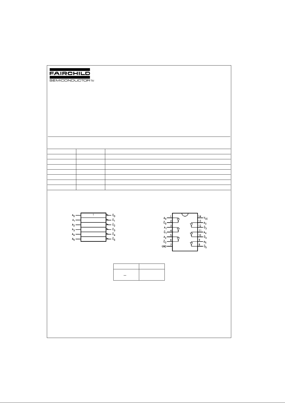
The AC/ACT04 contains six inverters.
Features
■ ICC reduced by 50% on 74AC only
■ Outputs source/sink 24 mA
■ ACT04 has TTL-compatible inputs
Ordering Code:
Device also available in Tape and Reel. Specify by appending suffix letter “X” to the ordering code. (PC not available in Tape and Reel.)
Logic Symbol
IEEE/IEC
Connection Diagram
Pin Descriptions
FACT is a trademark of Fairchild Semiconductor Corporation.
Order Number Package Number Package Description
74AC04SC M14A 14-Lead Small Outline Integrated Circuit (SOIC), JEDEC MS-120, 0.150” Narrow Body
74AC04SJ M14D 14-Lead Small Outline Package (SOP), EIAJ TYPE II, 5.3mm Wide
74AC04MTC MTC14 14-Lead Thin Shrink Small Outline Package (TSSOP), JEDEC MO-153, 4.4mm Wide
74AC04PC N14A 14-Lead Plastic Dual-In-Line Package (PDIP), JEDEC MS-001, 0.300” Wide
74ACT04SC M14A 14-Lead Small Outline Integrated Circuit (SOIC), JEDEC MS-120, 0.150” Narrow Body
74ACT04MTC MTC14 14-Lead Thin Shrink Small Outline Package (TSSOP), JEDEC MO-153, 4.4mm Wide
74ACT04PC N14A 14-Lead Plastic Dual-In-Line Package (PDIP), JEDEC MS-001, 0.300” Wide
Pin Names Description
A
n
Inputs
O
n
Outputs
Page 2
www.fairchildsemi.com 2
74AC04 • 74ACT04
Absolute Maximum Ratings(Note 1) Recommended Operating
Conditions
Note 1: Absolute maximum ratings are those values beyond which damage
to the device may occur. The databook specifications should be met, without exception, to ensure that the system design is reliable over its power
supply, temperature, and ou tput/inp ut loadi ng varia bles. Fairchild does no t
recommend operat ion of FACT circuits outside da t abook specifications.
DC Electrical Characteristics for AC
Note 2: All outputs loaded; thresholds on input assoc iat ed with output under tes t.
Note 3: Maximum test duratio n 2. 0 ms, one output loaded at a time.
Note 4: I
IN
and ICC @ 3.0V are guaranteed to be less than or equa l to th e respective limit @ 5.5V VCC.
Supply Voltage (VCC) −0.5V to +7.0V
DC Input Diode Current (I
IK
)
V
I
= −0.5V −20 mA
V
I
= VCC + 0.5V +20 mA
DC Input Voltage (V
I
) −0.5V to VCC + 0.5V
DC Output Diode Current (I
OK
)
V
O
= −0.5V −20 mA
V
O
= VCC + 0.5V +20 mA
DC Output Voltage (V
O
)
−0.5V toV
CC
+ 0.5V
DC Output Source or Sink Current (I
O
) ±50 mA
DC V
CC
or Ground Current
per Output Pin (I
CC
or I
GND
) ±50 mA
Storage Temperature (T
STG
) −65°C to +150°C
Junction Temperature (T
J
)
PDIP 140°C
Supply Voltage (V
CC
)
AC 2.0V to 6.0V
ACT 4.5V to 5.5V
Input Voltage (V
I
) 0V to V
CC
Output Voltage (VO) 0V to V
CC
Operating Temperature (TA) −40°C to +85°C
Minimum Input Edge Rate (∆V/∆t)
AC Devices
V
IN
from 30% to 70% of V
CC
VCC @ 3.3V, 4.5V, 5.5V 125 mV/ns
Minimum Input Edge Rate (∆V/∆t)
ACT Devices
V
IN
from 0.8V to 2.0V
V
CC
@ 4.5V, 5.5V 125 mV/ns
Symbol Parameter
V
CC
TA = +25°C
T
A
= −40°C to +85°C
Units Conditions
(V) Typ Guaranteed Limits
V
IH
Minimum HIGH Level 3.0 1.5 2.1 2.1 V
OUT
= 0.1V
Input Voltage 4.5 2.25 3.15 3.15 V or VCC − 0.1V
5.5 2.75 3.85 3.85
V
IL
Maximum LOW Level 3.0 1.5 0.9 0.9 V
OUT
= 0.1V
Input Voltage 4.5 2.25 1.35 1.35 V or VCC − 0.1V
5.5 2.75 1.65 1.65
V
OH
Minimum HIGH Level 3.0 2.99 2.9 2.9
Output Voltage 4.5 4.49 4.4 4.4 V I
OUT
= −50 µA
5.5 5.49 5.4 5.4
VIN= VILor V
IH
3.0 2.56 2.46 IOH = −12 mA
4.5 3.86 3.76 V I
OH
= −24 mA
5.5 4.86 4.76 I
OH
= −24 mA (Note 2)
V
OL
Maximum LOW Level 3.0 0.002 0.1 0.1
Output Voltage 4.5 0.001 0.1 0.1 V I
OUT
= 50 µA
5.5 0.001 0.1 0.1
VIN= VILor V
IH
3.0 0.36 0.44 IOL= 12 mA
4.5 0.36 0.44 V IOL = 24 mA
5.5 0.36 0.44 IOL = 24 mA (Note 2)
IIN Maximum Input
5.5 ±0.1 ±1.0 µAVI = VCC, GND
(Note 4) Leakage Current
I
OLD
Minimum Dynamic Output Current 5.5 75 mA V
OLD
= 1.65V Max
I
OHD
(Note 3) 5.5 −75 mA V
OHD
= 3.85V Min
ICC Maximum Quiescent
5.5 2.0 20.0 µA
VIN = V
CC
(Note 4) Supply Current or GND
Page 3
3 www.fairchildsemi.com
74AC04 • 74ACT04
DC Electrical Characteristics for ACT
Note 5: All outputs loaded; thres holds on input associate d w it h output under test.
Note 6: Maximum test duration 2.0 ms, one output loaded at a time.
Symbol Parameter
V
CC
TA = +25°CTA = −40°C to +85°C
Units Conditions
(V) Typ Guaranteed Limits
V
IH
Minimum HIGH Level 4.5 1.5 2.0 2.0
V
V
OUT
= 0.1V
Input Voltage 5.5 1.5 2.0 2.0 or VCC − 0.1V
V
IL
Maximum LOW Level 4.5 1.5 0.8 0.8
V
V
OUT
= 0.1V
Input Voltage 5.5 1.5 0.8 0.8 or V
CC
− 0.1V
V
OH
Minimum HIGH Level 4.5 4.49 4.4 4.4
VI
OUT
= −50 µA
Output Voltage 5.5 5.49 5.4 5.4
VIN = VIL or V
IH
4.5 3.86 3.76
V
IOH = −24 mA
5.5 4.86 4.76 I
OH
= −24 mA (Note 5)
V
OL
Maximum LOW Level 4.5 0.001 0.1 0.1
VI
OUT
= 50 µA
Output Voltage 5.5 0.001 0.1 0.1
VIN = VIL or V
IH
4.5 0.36 0.44
V
IOL0 = 24 mA
5.5 0.36 0.44 IOL = 24 mA (Note 5)
I
IN
Maximum Input
5.5 ±0.1 ±1.0 µAVI = VCC, GND
Leakage Current
I
CCT
Maximum
5.5 0.6 1.5 mA VI = VCC − 2.1V
ICC/Input
I
OLD
Minimum Dynamic Output Current 5.5 75 mA V
OLD
= 1.65V Max
I
OHD
(Note 6) 5.5 −75 mA V
OHD
= 3.85V Min
I
CC
Maximum Quiescent
5.5 4.0 40.0 µA
VIN = V
CC
Supply Current or GND
Page 4

www.fairchildsemi.com 4
74AC04 • 74ACT04
AC Electrical Characteristics for AC
Note 7: Voltage Range 3.3 is 3.3V ± 0.3V
Voltage Range 5.0 is 5.0V ± 0.5V
AC Electrical Characteristics for ACT
Note 8: Voltage Range 5.0 is 5.0V ± 0.5V
Capacitance
V
CC
TA = +25°CT
A
= −40°C to +85°C
Symbol Parameter (V)
C
L
= 50 p CL = 50 pF
Units
(Note 7) Min Typ Max Min Max
t
PLH
Propagation Delay 3.3 1.5 4.5 9.0 1.0 10.0
ns
5.0 1.5 4.0 7.0 1.0 7.5
t
PHL
Propagation Delay 3.3 1.5 4.5 8.5 1.0 9.5
ns
5.0 1.5 3.5 6.5 1.0 7.0
V
CC
TA = +25°CT
A
= −40°C to +85°C
Symbol Parameter (V)
C
L
= 50 pF CL = 50 pF
Units
(Note 8) Min Typ Max Min Max
t
PLH
Propagation Delay 5.0 1.0 6.0 8.5 1.0 9.0 ns
t
PHL
Propagation Delay 5.0 1.0 5.5 8.0 1.0 8.5 ns
Symbol Parameter Typ Units Conditions
C
IN
Input Capacitance 4.5 pF VCC = OPEN
V
CC
Power Dissipation Capacitance 30.0 pF VCC = 5.0V
Page 5

5 www.fairchildsemi.com
74AC04 • 74ACT04
Physical Dimensions inches (millimeters) unless otherwise noted
14-Lead Small Outline Integrated Circuit (SOIC), JEDEC MS-120, 0.150” Narrow Body
Package Number M14A
Page 6

www.fairchildsemi.com 6
74AC04 • 74ACT04
Physical Dimensions inches (millimeters) unless otherwise noted (Continued)
14-Lead Small Outline Package (SOP), EIAJ TYPE II, 5.3mm Wide
Package Number M14D
Page 7

7 www.fairchildsemi.com
74AC04 • 74ACT04
Physical Dimensions inches (millimeters) unless otherwise noted (Continued)
14-Lead Thin Shrink Sm all Ou tline Pa ck age (TS SO P), JE DE C MO-153, 4.4mm Wide
Package Number MTC14
Page 8

www.fairchildsemi.com 8
74AC04 • 74ACT04 Hex Inverter
Physical Dimensions inches (millimeters) unless otherwise noted (Continued)
14-Lead Plastic Dual-In-Line Package (PDIP), JEDEC MS-001, 0.300” Wide
Package Number N14A
Fairchild does not assume any responsibility for use of any circuitr y described, no circuit patent licenses are implied and
Fairchild reserves the right at any time without notice to change said circuitry and specifications.
LIFE SUPPORT POLICY
FAIRCHILD’S PRODUCTS ARE NOT AUTHORIZED FOR USE AS CRITICAL COMPONENTS IN LIFE SUPPORT
DEVICES OR SYSTEMS WITHOUT THE EXPRESS WRITTEN APPROVAL OF THE PRESIDENT OF FAIRCHILD
SEMICONDUCTOR CORPORATION. As used herein:
1. Life support devices or systems are devices or syste ms
which, (a) are intended for surgical implant into the
body, or (b) support or sustain life, and (c) whose failure
to perform when properly used in accordance with
instructions for use provided in the labeling, can be reasonably expected to result in a significant inju ry to the
user.
2. A critical component in any compon ent of a lif e supp ort
device or system whose failure t o perform can be reasonably expected to ca use the failure of the life supp ort
device or system, or to affect its safety or effectiveness.
www.fairchildsemi.com
 Loading...