

Datasheet 74ABT899CSCX, 74ABT899CSC, 74ABT899CQCX, 74ABT899CQC, 74ABT899CMSAX Datasheet (Fairchild Semiconductor)
...Page 1
November 1992
Revised January 1999
74ABT899 9-Bit Latchable Transceiver with Parity Generator/Checker
© 1999 Fairchild Semiconductor Corporation DS011509.prf www.fairchildsemi.com
74ABT899
9-Bit Latchable Transceiver
with Parity Generator/Checker
General Description
The ABT899 is a 9-bit to 9- bit par ity transcei ver with transparent latches. The d evice can operate as a feed-through
transceiver or it can generate/ check parity from the 8-bit
data busses in either direction.
The ABT899 features inde pende nt la tch ena bles for the Ato-B direction and the B-to-A direction, a select pin for
ODD/EVEN
parity, and separate error signal output pins for
checking parity.
Features
■ Latchable transceiver with output sink of 64 mA
■ Option to select generate parity and check or
“feed-through” data/parity in directions A-to-B or B-to-A
■ Independent latch enables for A-to-B and B-to-A
directions
■ Select pin for ODD/EVEN
parity
■ ERRA
and ERRB output pins for parity checking
■ Ability to simultaneously generate and check parity
■ May be used in systems applications in place of the
543 and 280
■ May be used in system applications in place of the
657 and 373 (no need to change T/R
to check parity)
■ Guaranteed output skew
■ Guaranteed multiple output switching specifications
■ Output switching specified for both 50 pF and
250 pF loads
■ Guaranteed simultaneous switching noise level and
dynamic threshold performance
■ Guaranteed latchup protection
■ High impedance glitch free bus loading during entire
power up and power down cycle
■ Nondestructive hot insertion capability
■ Disable time less than enable time to avoid bus
contention
Ordering Code:
Devices also available in Tape and Reel. Specify by appending suffix letter “X” to the ordering code.
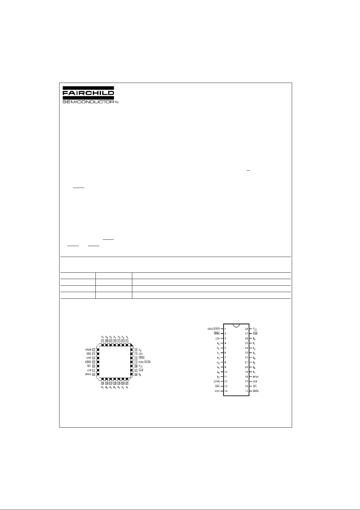
Connection Diagrams
Pin Assignment
for PLCC
Pin Assignment f or
SOIC and SSOP
Order Number Package Number Package Description
74ABT899CSC M28B 28-Lead Small Outline Integrated Circuit (SOIC), MS-013, 0.300” Wide Body
74ABT899CMSA MSA28 28-Lead Shrink Small Outline Package (SSOP), EIAJ TYPE II, 5.3mm Wide
74ABT899CQC V28A 28-Lead Plastic Lead Chip Carrier (PLCC), JEDEC MO-047, 0.450” Square
Page 2
www.fairchildsemi.com 2
74ABT899
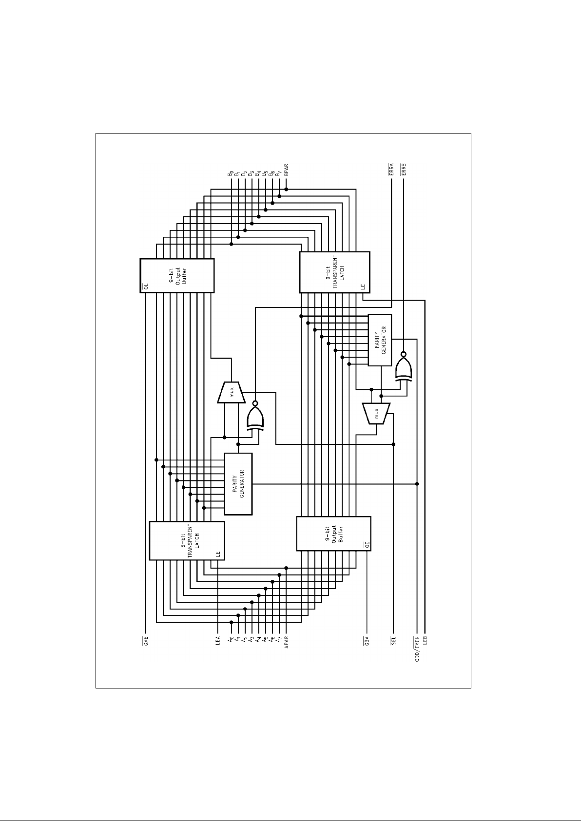
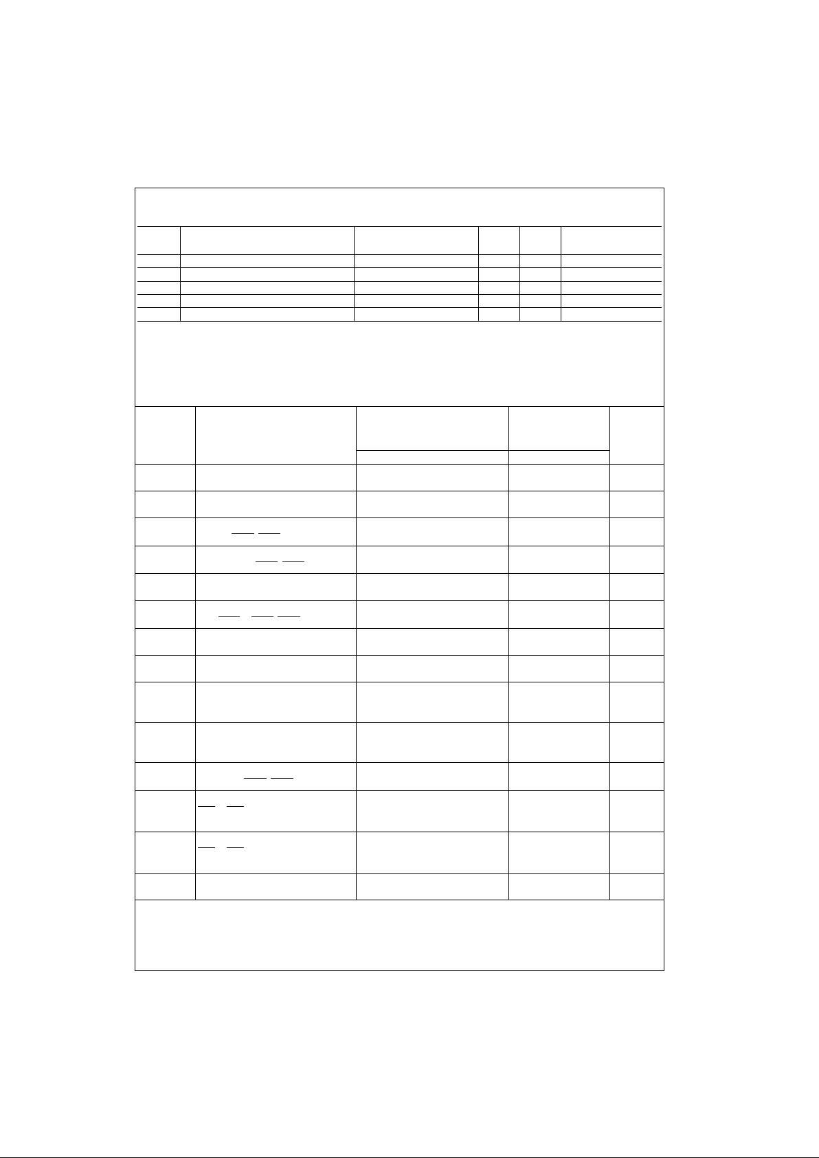
Pin Descriptions Functional Description
The ABT899 has three prin cipa l mode s of op erat ion w hich
are outlined below. These modes apply t o both the A- to-B
and B-to-A directions.
• Bus A (B) communicates to Bus B ( A), parity is generated and passed on to the B (A) Bus as BPAR (APAR). If
LEB (LEA) is HIGH and t he Mode Sele ct ( SEL
) is LOW,
the parity generated from B[0:7] (A[0:7]) can be checked
and monitored by ERRB
(ERRA).
• Bus A (B) communicates to Bus B (A) in a feed-through
mode if SEL
is HIGH. Parity is still generated and
checked as ERRA
and ERRB in the feed-th rough mo de
(can be used as an interru pt to signal a data/parity bit
error to the CPU).
• Independent Latch E nables (LEA and LEB) allow oth er
permutations of generating/checking (see Function
Table below).
Function Table
H = HIGH Voltage Level
L = LOW V oltage Level
X = Immaterial
Note 1: O/E
= ODD/EVEN
Pin Names Descriptions
A
0–A7
A Bus Data Inputs/Data Outputs
B
0–B7
B Bus Data Inputs/Data Outputs
APAR, BPAR A and B Bus Parity Inputs/Outputs
ODD/EVEN
ODD/EVEN Parity Select,
Active LOW fo r EVEN Parity
GBA
, GAB Output Enables for A or B Bus,
Active LOW
SEL
Select Pin for Feed-Through or
Generate Mode, LOW for Generate
Mode
LEA, LEB Latch Enables for A and B Latches,
HIGH for Transparent Mode
ERRA
, ERRB Error Signals for Checking Generated
Parity with Parity In, LOW if Error
Occurs
Inputs Operation
GAB
GBA SEL LEA LEB
H H X X X Busses A and B are 3-STATE.
H L L L H Generates parity from B[0:7] based on O/E
(Note 1). Generated parity → APAR.
Generated parity checked against BPAR and output as ERRB
.
HLLHH
Generates parity from B[0:7] based on O/E
. Generated parity → APAR. Gener-
ated parity checked against BPAR and output as ERRB
. Generated parity also
fed back through the A latch for generate/check as ERRA
.
HLLXL
Generates parity from B latch data based on O/E
. Generated parity → APAR.
Generated parity checked against latched BPAR and output as ERRB
.
H L H X H BPAR/B[0:7] → APAR/A0:7] Feed-through mode. Generated parity checked
against BPAR and output as ERRB
.
H L H H H BPAR/B[0:7] → APAR/A[0:7]
Feed-through mode. Generated parity checked against BPAR and output as
ERRB
. Generated parity also fed back through the A latch for generate/check as
ERRA
.
LHLHL
Generates parity for A[0:7] based on O/E
. Generated parity → BPAR. Gener-
ated parity checked against APAR and output as ERRA
.
LHLHH
Generates parity from A[0:7] based on O/E
. Generated parity → BPAR. Gener-
ated parity checked against APAR and output as ERRA
. Generated parity also
fed back through the B latch for generate/check as ERRB
.
LHLLX
Generates parity from A latch data based on O/E
. Generated parity → BPAR.
Generated parity checked against latched APAR and output as ERRA
.
L H H H L AP AR/A[0:7] → BPAR/B[0:7]
Feed-through mode. Generated parity checked against APAR and output as
ERRA
.
L H H H H APAR/A[0:7] → BPAR/B[0:7]
Feed-through mode. Generated parity checked against APAR and output as
ERRA
. Generated parity also fed back through the B latch for generate/check as
ERRB
.
Page 3
3 www.fairchildsemi.com
74ABT899
Functional Block Diagram
Page 4
www.fairchildsemi.com 4
74ABT899
Absolute Maximum Ratings(Note 2)
Recommended Operating
Conditions
Note 2: Absolute maximum ratings are values beyond which the device
may be damaged or have its useful life impaired. Functional operation
under these conditi ons is not implied.
Note 3: Either voltage limit or current limit is s uf f ic ient to protect inputs.
DC Electrical Characteristics
Note 4: Guaranteed, but not tested.
Note 5: Add 3.75 mA for each ERR
LOW.
Storage Temperature −65°C to +150°C
Ambient Temperature under Bias −55°C to +125°C
Junction Temperature under Bias
Plastic −55°C to +150°C
V
CC
Pin Potential to
Ground Pin −0.5V to +7.0V
Input Voltage (Note 3) −0.5V to +7.0V
Input Current (Note 3) −30 mA to +5.0 mA
Voltage Applied to Any Output
in the Disable or PowerOff State −0.5V to +5.5V
in the HIGH State −0.5V to V
CC
Current Applied to Output
in LOW State (Max)
twice therated I
OL
(mA)
DC Latchup Source Current −500 mA
Over Voltage Latchup (I/O) 10V
Free Air Ambient Temperature −40°C to +85°C
Supply Voltage +4.5V to +5.5V
Minimum Input Edge Rate (∆V/∆t)
Data Input 50 mV/ns
Enable Input 20 mV/ns
Symbol Parameter Min Typ Max Units
V
CC
Conditions
V
IH
Input HIGH Voltage 2.0 V Recognized HIGH Signal
V
IL
Input LOW Voltage 0.8 V Recognized LOW Signal
V
CD
Input Clamp Diode Voltage −1.2 V Min IIN = −18 mA (Non I/O Pins)
V
OH
Output HIGH 2.5 V Min IOH = −3 mA, (An, Bn, APAR, BPAR)
Voltage 2.0 IOH = −32 mA, (An, Bn, APAR, BPAR)
V
OL
Output LOW Voltage 0.55 V Min IOL = 64 mA, (An, Bn, APAR, BPAR)
V
ID
Input Leakage Te st 4.75 V 0.0 IID = 1.9 µA, (Non-I/O Pins)
All Other Pins Grounded
I
IH
Input HIGH Current 5 µAMaxVIN = 2.7V (Non-I/O Pins) (Note 4)
VIN = VCC (Non-I/O Pins)
I
BVI
Input HIGH Current 7 µAMaxVIN = 7.0V (Non-I/O Pins)
Breakdown Test
I
BVIT
Input HIGH Current 100 µAMaxVIN = 5.5V (An, Bn, APAR, BPAR)
Breakdown Test (I/O)
I
IL
Input LOW Current −5 µAMaxVIN = 0.5V (Non-I/O Pins) (Note 4)
VIN = 0.0V (Non-I/O Pins)
IIH + I
OZH
Output Leakage Current 50 µA 0V–5.5V V
OUT
= 2.7V (An, Bn);
GAB and GBA = 2.0V
IIL + I
OZL
Output Leakage Current −50 µA 0V–5.5V V
OUT
= 0.5V (An, Bn);
GAB and GBA = 2.0V
I
OS
Output Short-Circuit Current −100 −275 mA Max V
OUT
= 0V (An, Bn, APAR, BPAR)
I
CEX
Output HIGH Leakage Current 50 µAMaxV
OUT
= VCC (An, Bn, APAR, BPAR)
I
ZZ
Bus Drainage T est 100 µA0.0VV
OUT
= 5.5V (An, Bn, APAR, BPAR);
All Others GND
I
CCH
Power Supply Current 250 µA Max All Outputs HIGH
I
CCL
Power Supply Current 34 mA Max All Outputs LOW, ERRA/B = HIGH (Note 5)
I
CCZ
Power Supply Current 250 µA Max Outputs 3-STATE All Others at VCC or GND
I
CCT
Additional ICC/Input 2.5 mA Max VI = VCC − 2.1V All Others at VCC or GND
I
CCD
Dynamic ICC: No Load 0.4 mA/MHz Max Outputs Open
(Note 4)
GAB or GBA = GND, LE = HIGH
Non-I/O = GND or V
CC
One bit toggling, 50% duty cycle
Page 5
5 www.fairchildsemi.com
74ABT899
DC Electrical Characteristics
(PLCC package)
Note 6: Max number of ou t puts defined as (n). n − 1 data inputs are driven 0V to 3V. One output at LOW. Guaranteed, but not tested.
Note 7: Max number o f dat a inp uts (n) switchi ng. n − 1 in put s switchin g 0V t o 3V. Input-under-tes t switchi ng: 3 V to th resh old (V
ILD
), 0V to threshold (V
IHD
).
Guaranteed, but not tested.
Note 8: Max number of ou t puts defined as (n). n − 1 data inpu t s a re driven 0V to 3V. One output HIGH. Guaranteed, but not tested.
AC Electrical Characteristics
(SOIC and PLCC Package)
Symbol Parameter Min Typ Max Units
V
CC
Conditions
CL = 50 pF, RL = 500Ω
V
OLP
Quiet Output Maximum Dynamic V
OL
0.8 1.1 V 5.0 TA = 25°C (Note 6)
V
OLV
Quiet Output Minimum Dynamic V
OL
−1.3 −0.8 V 5.0 TA = 25°C (Note 6)
V
OHV
Minimum HIGH Level Dynamic Output Voltage 2.5 3.0 V 5.0 TA = 25°C (Note 8)
V
IHD
Minimum HIGH Level Dynamic Input Voltage 2.2 1.8 V 5.0 TA = 25°C (Note 7)
V
ILD
Maximum LOW Level Dynamic Input Voltage 0.8 0.5 V 5.0 TA = 25°C (Note 7)
Symbol Parameter
TA = +25°CT
A
= −40°C to +85°C
Units
VCC = +5.0V VCC = 4.5V–5.5V
CL = 50 pF CL = 50 pF
Min Typ Max Min Max
t
PLH
Propagation Delay 1.5 3.0 4.8 1.5 4.8 ns
t
PHL
An, to B
n
1.5 3.5 4.8 1.5 4.8
t
PLH
Propagation Delay 2.5 5.9 9.2 2.5 9.2 ns
t
PHL
An, Bn to BPAR, APAR 2.5 5.8 9.2 2.5 9.2
t
PLH
Propagation Delay 2.5 5.4 8.5 2.5 8.5 ns
t
PHL
An, Bn to ERRA, ERRB
2.5 5.4 8.5 2.5 8.5
t
PLH
Propagation Delay 1.5 3.7 6.0 1.5 6.0 ns
t
PHL
APAR, BPAR to ERRA, ERRB
1.5 3.7 6.0 1.5 6.0
t
PLH
Propagation Delay 2.0 4.4 6.9 2.0 6.9 ns
t
PHL
ODD/EVEN to APAR, BPAR 2.0 4.4 6.9 2.0 6.9
t
PLH
Propagation Delay 1.8 4.0 6.0 1.8 6.0 ns
t
PHL
ODD/EVEN to ERRA, ERRB
1.8 4.0 6.0 1.8 6.0
t
PLH
Propagation Delay 1.5 3.8 6.0 1.5 6.0 ns
t
PHL
SEL to APAR, BPAR 1.5 3.8 6.0 1.5 6.0
t
PLH
Propagation Delay 1.5 3.2 4.6 1.5 4.6 ns
t
PHL
LEA, LEB to Bn, A
n
1.5 3.2 4.6 1.5 4.6
t
PLH
Propagation Delay 2.5 5.9 8.8 2.5 8.8
nst
PHL
LEA, LEB to BPAR, APAR 2.5 5.7 8.8 2.5 8.8
Generate Mode
t
PLH
Propagation Delay 1.5 3.6 5.1 1.5 5.1 ns
t
PHL
LEA, LEB to BPAR, APAR, 1.5 3.6 5.1 1.5 5.1
Feed Thru Mode
t
PLH
Propagation Delay 1.6 5.4 8.4 1.6 8.4 ns
t
PHL
LEA, LEB to ERRA, ERRB
1.6 5.4 8.4 1.6 8.4
t
PZH
Output Enable Time 1.5 3.6 6.0 1.5 6.0 ns
t
PZL
GBA or GAB to An,
1.5 3.4 6.0 1.5 6.0
APAR or Bn, BPAR
t
PHZ
Output Disable Time 1.0 4.0 6.0 1.0 6.0 ns
t
PLZ
GBA or GAB to An,
1.0 3.3 6.0 1.0 6.0
APAR or Bn, BPAR
t
PLHtPHL
Propagation Delay 1.5 3.3 5.4 1.5 5.4 ns
APAR to BPAR, BPAR to APAR 1.5 3.8 5.4 1.5 5.4
Page 6

www.fairchildsemi.com 6
74ABT899
AC Electrical Charac teristics
(SSOP Package)
AC Operating Requirements
Symbol Parameter
TA = +25°CT
A
= −40°C to +85°C
Units
VCC = +5.0V VCC = 4.5V–5.5V
CL = 50 pF CL = 50 pF
Min Typ Max Min Max
t
PLH
Propagation Delay 1.5 3.0 5.3 1.5 5.3 ns
t
PHL
An, to B
n
1.53.55.31.55.3
t
PLH
Propagation Delay 2.5 5.9 9.9 2.5 9.9 ns
t
PHL
An, Bn to BPAR, APAR 2.5 5.8 9.9 2.5 9.9
t
PLH
Propagation Delay 2.5 5.4 9.4 2.5 9.4 ns
t
PHL
An, Bn to ERRA, ERRB
2.55.49.42.59.4
t
PLH
Propagation Delay 1.5 3.7 6.5 1.5 6.5 ns
t
PHL
APAR, BPAR to ERRA, ERRB
1.53.76.51.56.5
t
PLH
Propagation Delay 2.0 4.4 7.4 2.0 7.4 ns
t
PHL
ODD/EVEN to APAR, BPAR 2.0 4.4 7.4 2.0 7.4
t
PLH
Propagation Delay 1.8 4.0 6.5 1.8 6.5 ns
t
PHL
ODD/EVEN to ERRA, ERRB
1.84.06.51.86.5
t
PLH
Propagation Delay 1.5 3.8 6.5 1.5 6.5 ns
t
PHL
SEL to APAR, BPAR 1.5 3.8 6.5 1.5 6.5
t
PLH
Propagation Delay 1.5 3.2 5.1 1.5 5.1 ns
t
PHL
LEA, LEB to Bn, A
n
1.53.25.11.55.1
t
PLH
Propagation Delay 2.5 5.9 9.2 2.5 9.2
nst
PHL
LEA, LEB to BPAR, APAR 2.5 5.7 9.2 2.5 9.2
Generate Mode
t
PLH
Propagation Delay 1.5 3.6 5.6 1.5 5.6 ns
t
PHL
LEA, LEB to BPAR, APAR, 1.5 3.6 5.6 1.5 5.6
Feed Thru Mode
t
PLH
Propagation Delay 1.6 5.4 8.9 1.6 8.9 ns
t
PHL
LEA, LEB to ERRA, ERRB
1.65.48.91.68.9
t
PZH
Output Enable Time 1.5 3.6 6.5 1.5 6.5 ns
t
PZL
GBA or GAB to An,
1.53.46.51.56.5
APAR or Bn, BPAR
t
PHZ
Output Disable Time 1.0 4.0 6.5 1.0 6.5 ns
t
PLZ
GBA or GAB to An,
1.03.36.51.06.5
APAR or Bn, BPAR
t
PLH
Propagation Delay 1.5 3.3 5.9 1.5 5.9 ns
t
PHL
APAR to BPAR, BPAR to APAR 1.5 3.8 5.9 1.5 5.9
Symbol Parameter
TA = +25°CT
A
= −40°C to +85°C
Units
VCC = +5.0V VCC = 4.5V–5.5V
CL = 50 pF CL = 50 pF
Min Max Min Max
tS(H) Setup Time, HIGH or LOW An,1.5 1.5 ns
tS(L) APAR to LEA or Bn, BPAR to LEB 1.5 1.5
tH(H) Hold Time, HIGH or LOW An,1.0 1.0 ns
tH(L) APAR to LEA or Bn, BPAR to LEB 1.0 1.0
tW(H) Pulse Width, HIGH 3.0 3.0 ns
LEA or LEB
Page 7

7 www.fairchildsemi.com
74ABT899
Extended AC Electri cal Characteristics
(SOIC and PLCC Package)
Note 9: This specification is guarantee d but not tested . The limits ap ply to propaga tion delays for all paths de scribe d switching in phas e (i.e., all LOW-toHIGH, HIGH-to-LOW, et c.) .
Note 10: This specification is guaranteed but not tested. The limits represent propagation delay with 250 pF load capacitors in place of the 50 pF load capacitors in the standard AC load . Th is sp ec if ic ation pertains to sin gle output switching only.
Note 11: This specific at ion is guaranteed but not tested. The limi ts represent propag at ion delays for all paths des c ribed switching in phase (i.e., all LOW-toHIGH, HIGH-to-LOW, etc.) with 250 pF load capacitors in place of th e 50 pF load capacitors in th e s ta ndard AC load
Note 12: The 3-STATE delay time is dominated by the RC network (500Ω, 250 pF) on the output and has bee n excluded from the datashee t.
Note 13: Not applicable for mult iple output switching.
Symbol Parameter
TA = +25°CT
A
= −40°C to +85°CTA = −40°C to +85°C
Units
VCC = +5.0V VCC = 4.5V–5.5V VCC = 4.5V–5.5V
CL = 50 pF CL = 250 pF CL = 250 pF
9 Outputs Switching 1 Output Switching 9 Outputs Switching
(Note 9) (Note 10) (Note 11)
Min Typ Max Min Max Min Max
f
TOGGLE
Max Toggle Frequency 100 MHz
t
PLH
Propagation Delay 1.5 6.2 2.0 7.2 2.5 9.5
ns
t
PHL
An to B
n
1.5 6.2 2.0 7.2 2.5 9.5
t
PLH
Propagation Delay 1.5 6.8 2.0 8.0 2.5 10.0 ns
t
PHL
APAR to BPAR 1.5 6.8 2.0 8.0 2.0 10.0
t
PLH
Propagation Delay 2.5 10.0 3.0 12.5 3.5 13.5 ns
t
PHL
An, Bn to BPAR, APAR 2.5 10.0 3.0 12.5 3.5 13.5
t
PLH
Propagation Delay (Note 13) 3.0 12.0 (Note 13) ns
t
PHL
An, Bn to ERRA, ERRB
3.0 12.0
t
PLH
Propagation Delay (Note 13) 2.0 9.0 (Note 13) ns
t
PHL
APAR, BPAR to ERRA, ERRB
2.0 9.0
t
PLH
Propagation Delay (Note 13) 2.5 9.9 (Note 13) ns
t
PHL
ODD/EVEN to APAR, BPAR 2.5 9.9
t
PLH
Propagation Delay (Note 13) 2.0 8.8 (Note 13) ns
t
PHL
ODD/EVEN to ERRA, ERRB
2.0 8.8
t
PLH
Propagation Delay (Note 13) 2.0 9.5 (Note 13) ns
t
PHL
SEL to APAR, BPAR 2.0 9.5
t
PLH
Propagation Delay 1.5 5.7 2.0 7.9 2.5 10.0 ns
t
PHL
LEA, LEB to Bn, A
n
1.5 5.7 2.0 7.9 2.5 10.0
t
PLH
Propagation Delay 1.5 9.5 2.0 12.0 2.5 13.0 ns
t
PHL
LEA, LEB to BPAR, APAR 1.5 9.5 2.0 12.0 2.5 13.0
t
PLH
Propagation Delay (Note 13) 2.0 11.5 (Note 13) ns
t
PHL
LEA, LEB to ERRA, ERRB
2.0 11.5
t
PZH
Output enable time 1.5 7.0 2.0 8.5 2.5 10.5
t
PZL
GBA or GAB to An,
1.5 7.0 2.0 8.5 2.5 10.5 ns
APAR or Bn, BPAR
t
PHZ
Output disable time 1.0 6.5
t
PLZ
GBA or GAB to An,
1.0 6.5 (Note 12) (Note 12) ns
APAR or Bn, BPAR
Page 8

www.fairchildsemi.com 8
74ABT899
Extended AC Electrical Characteristics
(SSOP Package)
Note 14: This spec ification is guarantee d but not tes ted. The limits app ly to propag ation de lays for all paths des cribe d switching in ph ase ( i.e., a ll LOW-toHIGH, HIGH-to-LOW, etc.).
Note 15: This specification is guaranteed but not tested. The limits represent propagation delay with 250 pF load capacitors in place of the 50 pF load capacitors in the standard AC lo ad. This specification pe rtains to single outp ut switching only.
Note 16: This specificat ion is guaranteed but not tested. The limits represent propag at ion delays for all paths desc ribed switching in phas e (i.e., all LOW-toHIGH, HIGH-to-L OW, etc.) with 250 p F load capacitors in place of the 50 pF load capacitors in the s ta ndard AC load
Note 17: The 3-STATE delay time is dominated by the RC network (500Ω, 250 pF) on the output and has been excluded from the datash eet .
Note 18: Not applicable for multiple output switching.
Symbol Parameter
TA = +25°CT
A
= −40°C to +85°CTA = −40°C to +85°C
Units
VCC = +5.0V VCC = 4.5V–5.5V VCC = 4.5V–5.5V
CL = 50 pF CL = 250 pF CL = 250 pF
9 Outputs Switching 1 Output Switching 9 Outputs Switching
(Note 14) (Note 15) (Note 16)
Min Typ Max Min Max Min Max
f
TOGGLE
Max Toggle Frequency 100 MHz
t
PLH
Propagation Delay 1.5 6.7 2.0 7.7 2.5 10.1
ns
t
PHL
An to B
n
1.5 6.7 2.0 7.7 2.5 10.1
t
PLH
Propagation Delay 1.5 7.3 2.0 8.5 2.5 10.6 ns
t
PHL
APAR to BPAR 1.5 7.3 2.0 8.5 2.0 10.6
t
PLH
Propagation Delay 2.5 10.7 3.0 13.2 3.5 14.3 ns
t
PHL
An, Bn to BPAR, APAR 2.5 10.7 3.0 13.2 3.5 14.3
t
PLH
Propagation Delay (Note 18) 3.0 12.9 (Note 18) ns
t
PHL
An, Bn to ERRA, ERRB
3.0 12.9
t
PLH
Propagation Delay (Note 18) 2.0 9.5 (Note 18) ns
t
PHL
APAR, BPAR to ERRA, ERRB
2.0 9.5
t
PLH
Propagation Delay (Note 18) 2.5 10.4 (Note 18) ns
t
PHL
ODD/EVEN to APAR, BPAR 2.5 10.4
t
PLH
Propagation Delay (Note 18) 2.0 9.3 (Note 18) ns
t
PHL
ODD/EVEN to ERRA, ERRB
2.0 9.3
t
PLH
Propagation Delay (Note 18) 2.0 10.0 (Note 18) ns
t
PHL
SEL to APAR, BPAR 2.0 10.0
t
PLH
Propagation Delay 1.5 6.2 2.0 8.4 2.5 10.6 ns
t
PHL
LEA, LEB to Bn, A
n
1.5 6.2 2.0 8.4 2.5 10.6
t
PLH
Propagation Delay 1.5 10.0 2.0 12.5 2.5 13.6 ns
t
PHL
LEA, LEB to BPAR, APAR 1.5 10.0 2.0 12.5 2.5 13.6
t
PLH
Propagation Delay (Note 18) 2.0 12.0 (Note 18) ns
t
PHL
LEA, LEB to ERRA, ERRB
2.0 12.0
t
PZH
Output enable time 1.5 7.5 2.0 9.0 2.5 11.1
t
PZL
GBA or GAB to An,
1.5 7.5 2.0 9.0 2.5 11.1 ns
APAR or Bn, BPAR
t
PHZ
Output disable time 1.0 7.0
t
PLZ
GBA or GAB to An,
1.0 7.0 (Note 17) (Note 17) ns
APAR or Bn, BPAR
Page 9

9 www.fairchildsemi.com
74ABT899
Skew
(PLCC package) (Note 2)
Note 19: This specific ation is gua ranteed but not tested . The limit s apply to propagat ion delays for all pa ths descr ibed switching in phase (i.e., all LOW-toHIGH, HIGH-to-LOW, et c.) .
Note 20: This spec ification is gua ranteed but not t ested. The lim its represent p ropagation d elays with 250 pF load capacitors in place of the 50 pF load
capacitors in the standard AC load.
Note 21: Skew is defined a s the ab solute value of t he dif ference bet ween the actu al propa gation delays for any two sepa rate ou tputs o f the same device.
The specification applies to any outputs swit c hing HIGH to LOW (t
OSHL
), LOW to HIGH (t
OSLH
), or any combination switching LOW to HIGH and/or HIGH to
LOW (t
OST
). This specificatio n is guaranteed but not tested. Skew applies to propagation del ays indiv idually; i.e., An to Bn separate from LEA to An.
Note 22: This descri bes the dif ference betwee n the delay of th e LOW-to-HIGH an d the HIGH -to-LOW trans ition on the same p in. It is measu red ac ross al l
the outputs (drivers) on th e s am e chip, the worst (largest delta) number is the guaranteed sp ec if ic at ion. This specification is guaranteed but not tested.
Note 23: Propagation delay variation for a given s et of conditions (i.e., tem perature and V
CC
) from device to device. T his specification is g uaranteed but not
tested.
Capacitance
Note 24: C
I/O
is measured at frequency, f = 1 MHz, per MIL-STD-883B, Method 3012.
Symbol Parameter
TA = −40°C to +85°CT
A
= −40°C to +85°C
Units
VCC = 4.5V–5.5V VCC = 4.5V–5.5V
CL = 50 pF CL = 250 pF
9 Outputs Switching 9 Outputs Switching
(Note 19) (Note 20)
Max Max
t
OSHL
Pin to Pin Skew 1.0 2.0 ns
(Note 21) HL Transitions
t
OSLH
Pin to Pin Skew 1.1 2.1 ns
(Note 21) LH Transitions
t
PS
Duty Cycle 2.0 3.5 ns
(Note 22) LH–HL Skew
t
OST
Pin to Pin Skew 2.0 3.5 ns
(Note 21) LH/HL Transitions
t
PV
Device to Device Skew 3.0 4.0 ns
(Note 23) LH/HL Transitions
Symbol Parameter Typ Units
Conditions
TA = 25°C
C
IN
Input Pin Capacitance 5.0 pF VCC = 0V
C
I/O
(Note 24) Output Capacitance 11.0 pF VCC = 5.0V
Page 10

www.fairchildsemi.com 10
74ABT899
AC Path
An, APAR → Bn, BPAR
(B
n
, BPAR → An, APAR)
FIGURE 1.
An → BPAR
(B
n
→ APAR)
FIGURE 2.
An → ERRA
(Bn → ERRB)
FIGURE 3.
O/E → ERRA
O/E → ERRB
FIGURE 4.
Page 11

11 www.fairchildsemi.com
74ABT899
AC Pat h (Continued)
O/E → BPAR
(O/E
→ APAR)
FIGURE 5.
APAR → ERRA
(BPAR → ERRB)
FIGURE 6.
FIGURE 7.
ZH, HZ
FIGURE 8.
Page 12

www.fairchildsemi.com 12
74ABT899
AC Path (Continued)
ZL, LZ
FIGURE 9.
SEL → BPAR
(SEL
→ APAR)
FIGURE 10.
LEA → BPAR, B[0:7]
(LEB → APAR, A[0:7])
FIGURE 11.
TS(H), TH(H)
LEA → APAR, A[0:7]
(LEB → BPAR, B[0:7])
FIGURE 12.
Page 13

13 www.fairchildsemi.com
74ABT899
AC Pat h (Continued)
TS(L), TH(L)
LEA → APAR, A[0:7]
(LEB → BPAR, B[0:7])
FIGURE 13.
FIGURE 14.
Page 14

www.fairchildsemi.com 14
74ABT899
AC Loading
*Includes jig and pr obe capacitance
FIGURE 15. Standard AC Test Load
V
M
= 1.5V
FIGURE 16.
Input Pulse Requirements
FIGURE 17. Test Input Signal Requirements
AC Waveforms
FIGURE 18. Propagation Delay Waveforms for
Inverting and Non-Inverting Functions
FIGURE 19. Propagation Delay,
Pulse Width Waveforms
FIGURE 20. 3-STATE Output HIGH
and LOW Enable and Disable Times
FIGURE 21. Setup Time, Hold Time
and Recovery Time Waveforms
Amplitude Rep. Rate t
W
t
r
t
f
3.0V 1 MHz 500 ns 2.5 ns 2.5 ns
Page 15

15 www.fairchildsemi.com
74ABT899
Physical Dimensions inches (millimeters) unless otherwise noted
28-Lead Small Outline Integrated Circuit (SOIC), MS-013, 0.300” Wide Body
Package Number M28B
28-Lead Shrink Small Outline Package (SSOP), EIAJ TYPE II, 5.3mm Wide
Package Number MSA28
Page 16

Fairchild does not assume any responsibility for use of any circuitry described, no circuit patent licenses are implied and Fairchild reserves the right at any time without notice to change said circuitry and specifications.
74ABT899 9-Bit Latchable Transceiver with Parity Generator/Checker
LIFE SUPPORT POLICY
FAIRCHILD’S PRODUCTS ARE NOT AUTHORIZED FOR USE AS CRITICAL COMPONENTS IN LIFE SUPPORT
DEVICES OR SYSTEMS WITHOUT THE EXPRESS WRITTEN APPROVAL OF THE PRESIDENT OF FAIRCHILD
SEMICONDUCTOR CORPORATION. As used herein:
1. Life support devices or system s ar e devices or syste ms
which, (a) are intended for surgical implant into the
body, or (b) support or sustain life, and (c) whose failure
to perform when properly used in accordance with
instructions for use provided in the labeling, can be reasonably expected to result in a significant injury to the
user.
2. A critical component in any c omponent of a life suppor t
device or system whose failure to perform can be reasonably expected to cause the failure of the life suppor t
device or system, or to affect its safety or effectiveness.
www.fairchildsemi.com
Physical Dimensions inches (millimeters) unless otherwise noted (Continued)
28-Lead Plastic Lead Chip Carrier (PLCC), JEDEC MO-047, 0.450” Square
Package Number V28A
 Loading...