

Datasheet 74ABT240PW, 74ABT240N, 74ABT240DB, 74ABT240D, 74ABT240-1N Datasheet (Philips)
...Page 1
Philips Semiconductors Product specification
74ABT240Octal inverting buffer (3-State)
2
1996 Sep 10 853–1608 17274
FEATURES
•Octal bus interface
•3-State buffers
•Output capability: +64mA/–32mA
•Latch-up protection exceeds 500mA per Jedec Std 17
•ESD protection exceeds 2000 V per MIL STD 883 Method 3015
and 200 V per Machine Model
•Power-up 3-State
•Live insertion/extraction permitted
DESCRIPTION
The 74ABT240 high-performance BiCMOS device combines low
static and dynamic power dissipation with high speed and high
output drive.
The 74ABT240 device is an octal inverting buffer that is ideal for
driving bus lines. The device features two Output Enables (1OE
,
2OE
), each controlling four of the 3-State outputs.
QUICK REFERENCE DATA
SYMBOL PARAMETER
CONDITIONS
T
amb
= 25°C; GND = 0V
TYPICAL UNIT
t
PLH
t
PHL
Propagation delay
nAx to nY
x
CL = 50pF; VCC = 5V 3.1 ns
C
IN
Input capacitance VI = 0V or V
CC
4 pF
C
OUT
Output capacitance Outputs disabled; VO = 0V or V
CC
7 pF
I
CCZ
Total supply current Outputs disabled; VCC =5.5V 50 µA
ORDERING INFORMATION
PACKAGES TEMPERATURE RANGE OUTSIDE NORTH AMERICA NORTH AMERICA DWG NUMBER
20-Pin Plastic DIP –40°C to +85°C 74ABT240 N 74ABT240 N SOT146-1
20-Pin plastic SO –40°C to +85°C 74ABT240 D 74ABT240 D SOT163-1
20-Pin Plastic SSOP Type II –40°C to +85°C 74ABT240 DB 74ABT240 DB SOT339-1
20-Pin PlasticTSSOP Type I –40°C to +85°C 74ABT240 PW 74ABT240PW DH SOT360-1
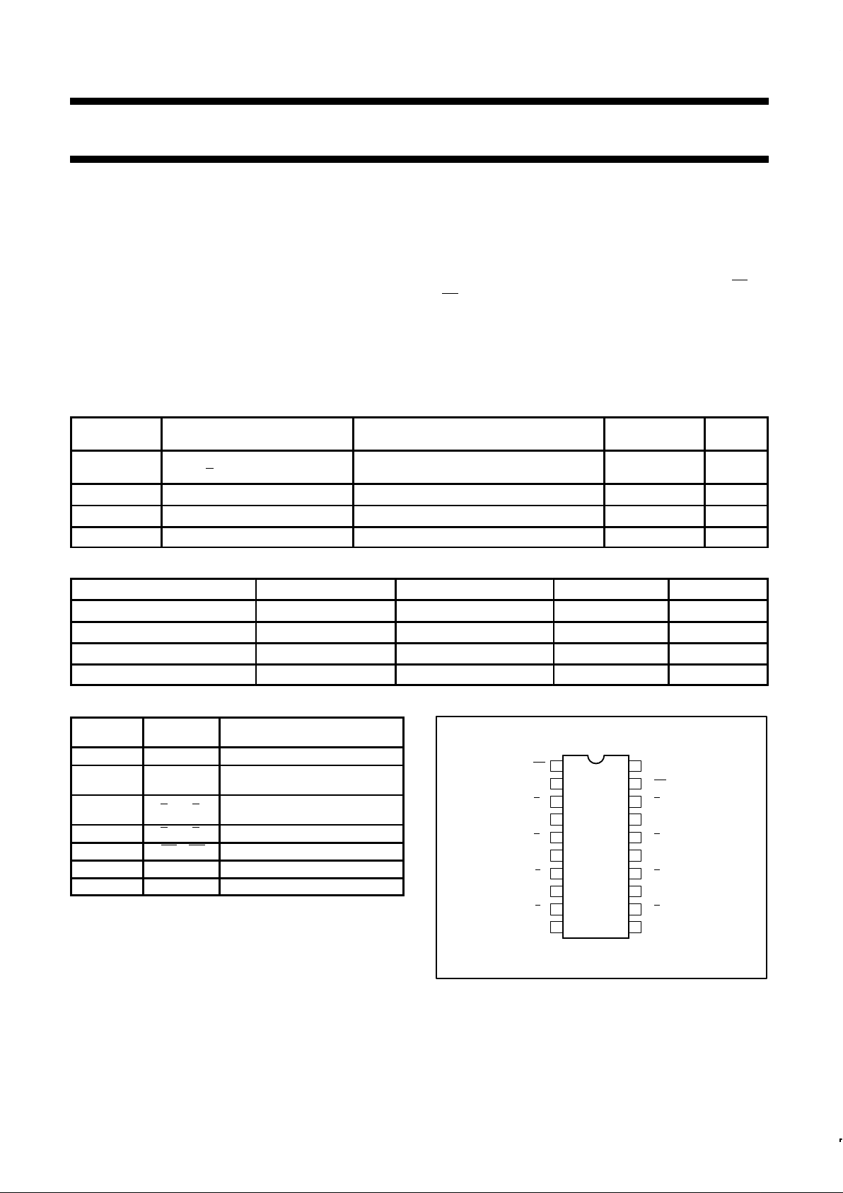
PIN DESCRIPTION
PIN
NUMBER
SYMBOL NAME AND FUNCTION
2, 4, 6, 8 1A0 – 1A3 Data inputs
11, 13, 15,
17
2A0 – 2A3 Data inputs
18, 16, 14,
12
1Y0 – 1Y3 Data outputs
9, 7, 5, 3 2Y0 – 2Y3 Data outputs
1, 19 1OE, 2OE Output enables
10 GND Ground (0V)
20 V
CC
Positive supply voltage
PIN CONFIGURATION
1
2
3
4
5
6
7
8
9
10 11
12
13
14
15
16
17
18
19
20
1OE
1A0
2Y
0
1A1
2Y
1
1A2
2Y
2
1A3
2Y
3 1Y3
GND
2A2
1Y
2
2A1
1Y
1
2A0
1Y
0
2OE
V
CC
2A3
SA00034
Page 2
Philips Semiconductors Product specification
74ABT240Octal inverting buffer (3-State)
1996 Sep 10
3
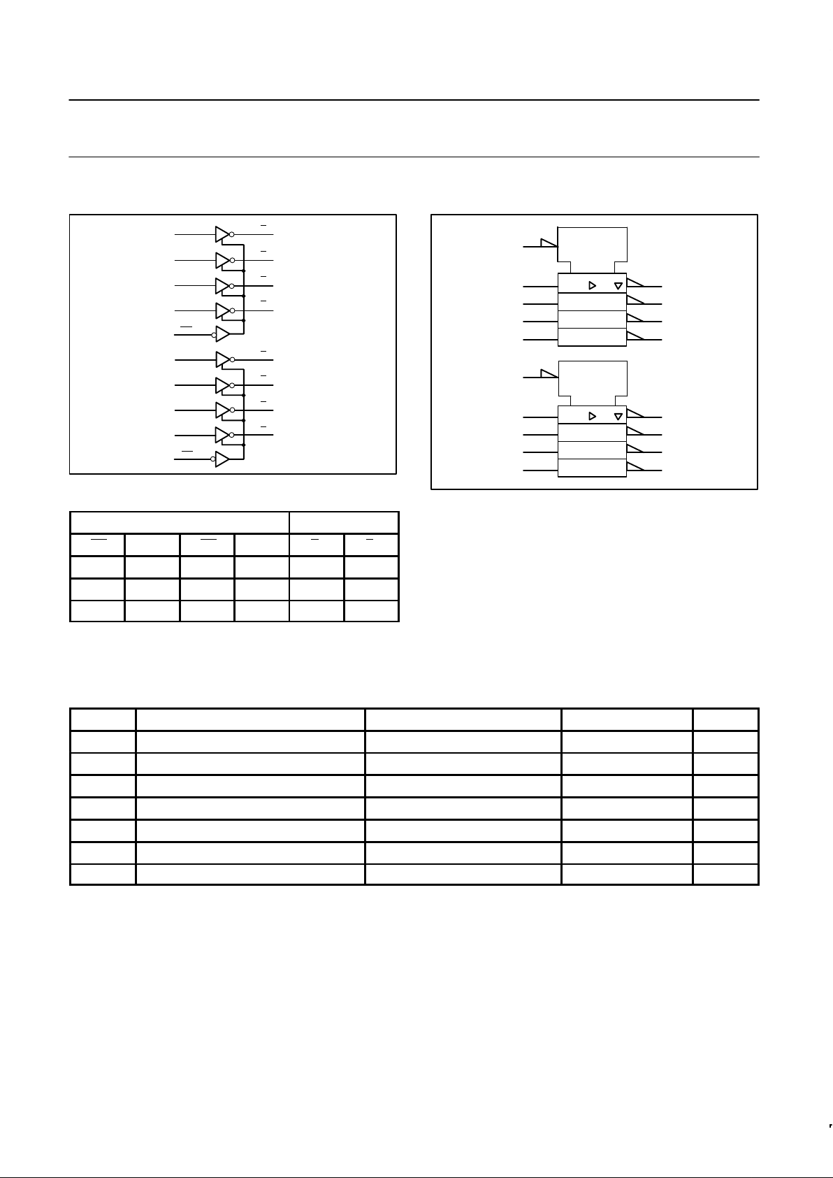
LOGIC SYMBOL
1
1A0
2
1A1
4
1A2
6
1A3
8
2OE
19
2A0
11
13
15
17
2A1
18
2A2
16
2A3
14
12
1Y
0
1Y
1
1Y
2
1Y
3
2Y0
2Y
1
2Y
2
2Y
3
9
7
5
3
1OE
SA00035
FUNCTION TABLE
INPUTS OUTPUTS
1OE 1An 2OE 2An 1Yn 2Yn
L L L L H H
L H L H L L
H X H X Z Z
H =High voltage level
L =Low voltage level
X = Don’t care
Z =High impedance ”off” state
LOGIC SYMBOL (IEEE/IEC)
EN
1
2
18
4
16
6
14
8
12
19
11
9
13
7
15
5
17
3
EN
SA00036
ABSOLUTE MAXIMUM RATINGS
1, 2
SYMBOL
PARAMETER CONDITIONS RATING UNIT
V
CC
DC supply voltage –0.5 to +7.0 V
I
IK
DC input diode current VI < 0 –18 mA
V
I
DC input voltage
3
–1.2 to +7.0 V
I
OK
DC output diode current VO < 0 –50 mA
V
OUT
DC output voltage
3
output in Off or High state –0.5 to +5.5 V
I
OUT
DC output current output in Low state 128 mA
T
stg
Storage temperature range –65 to 150 °C
NOTES:
1. Stresses beyond those listed may cause permanent damage to the device. These are stress ratings only and functional operation of the
device at these or any other conditions beyond those indicated under “recommended operating conditions” is not implied. Exposure to
absolute-maximum-rated conditions for extended periods may affect device reliability.
2. The performance capability of a high-performance integrated circuit in conjunction with its thermal environment can create junction
temperatures which are detrimental to reliability. The maximum junction temperature of this integrated circuit should not exceed 150°C.
3. The input and output voltage ratings may be exceeded if the input and output current ratings are observed.
Page 3

Philips Semiconductors Product specification
74ABT240Octal inverting buffer (3-State)
1996 Sep 10
4
RECOMMENDED OPERATING CONDITIONS
LIMITS
SYMBOL
PARAMETER
Min Max
UNIT
V
CC
DC supply voltage 4.5 5.5 V
V
I
Input voltage 0 V
CC
V
V
IH
High-level input voltage 2.0 V
V
IL
Low-level Input voltage 0.8 V
I
OH
High-level output current –32 mA
I
OL
Low-level output current 64 mA
∆t/∆v Input transition rise or fall rate 0 10 ns/V
T
amb
Operating free-air temperature range –40 +85 °C
DC ELECTRICAL CHARACTERISTICS
LIMITS
SYMBOL PARAMETER TEST CONDITIONS T
amb
= +25°C
T
amb
= –40°C
to +85°C
UNIT
Min Typ Max Min Max
V
IK
Input clamp voltage VCC = 4.5V; IIK = –18mA –0.9 –1.2 –1.2 V
VCC = 4.5V; IOH = –3mA; VI = VIL or V
IH
2.5 2.9 2.5 V
V
OH
High-level output voltage VCC = 5.0V; IOH = –3mA; VI = VIL or V
IH
3.0 3.4 3.0 V
VCC = 4.5V; IOH = –32mA; VI = VIL or V
IH
2.0 2.4 2.0 V
V
OL
Low-level output voltage VCC = 4.5V; IOL = 64mA; VI = VIL or V
IH
0.42 0.55 0.55 V
I
I
Input leakage current VCC = 5.5V; VI = GND or 5.5V ±0.01 ±1.0 ±1.0 µA
I
OFF
Power-off leakage current VCC = 0.0V; VI or VO ≤ 4.5V; ±5.0 ±100 ±100 µA
IPU/I
PD
Power-up/down 3-state
output current
3
VCC = 2.1V; VO = 0.5V; VI = GND or VCC;
V
OE
= Don’t care
±5.0 ±50 ±50 µA
I
OZH
3-State output High current VCC = 5.5V; VO = 2.7V; VI = VIL or V
IH
5.0 50 50 µA
I
OZL
3-State output Low current VCC = 5.5V; VO = 0.5V; VI = VIL or V
IH
–5.0 –50 –50 µA
I
CEX
Output High leakage current VCC = 5.5V; VO = 5.5V; VI = GND or V
CC
5.0 50 50 µA
I
O
Output current
1
VCC = 5.5V; VO = 2.5V –50 –100 –180 –50 –180 mA
I
CCH
VCC = 5.5V; Outputs High, VI = GND or V
CC
50 250 250 µA
I
CCL
Quiescent supply current VCC = 5.5V; Outputs Low, VI = GND or V
CC
24 30 30 mA
I
CCZ
VCC = 5.5V; Outputs 3-State;
V
I
= GND or V
CC
50 250 250 µA
∆I
CC
Additional supply current per
input pin
2
Outputs 3-State, one input at 3.4V , other
inputs at V
CC
or GND; VCC = 5.5V
0.5 1.5 1.5 mA
NOTES:
1. Not more than one output should be tested at a time, and the duration of the test should not exceed one second.
2. This is the increase in supply current for each input at 3.4V.
3. This parameter is valid for any V
CC
between 0V and 2.1V, with a transition time of up to 10msec. From VCC = 2.1V to VCC 5V ± 10% a
transition time of up to 100µsec is permitted.
Page 4

Philips Semiconductors Product specification
74ABT240Octal inverting buffer (3-State)
1996 Sep 10
5
AC CHARACTERISTICS
GND = 0V; tR = tF = 2.5ns; CL = 50pF, RL = 500Ω
LIMITS
SYMBOL PARAMETER WAVEFORM
T
amb
= +25°C
V
CC
= +5.0V
T
amb
= –40°C to +85°C
V
CC
= +5.0V ±0.5V
UNIT
Min Typ Max Min Max
t
PLH
t
PHL
Propagation delay
nAx to nY
x
1
1.0
1.6
2.7
3.5
4.1
4.3
1.0
1.6
4.8
4.8
ns
t
PZH
t
PZL
Output enable time
to High and Low level
2
1.1
1.1
3.1
4.2
4.7
5.8
1.1
1.1
5.2
6.2
ns
t
PHZ
t
PLZ
Output disable time
from High and Low level
2
1.8
1.6
3.7
3.0
5.7
5.4
1.8
1.6
6.4
5.8
ns
AC WAVEFORMS
VM = 1.5V, VIN = GND to 3.0V
nAx INPUT
V
M
V
M
nYx OUTPUT
V
M
V
M
t
PHL
t
PLH
SA00037
Waveform 1. Waveforms Showing the Input (nAx) to
Output (nY
x) Propagation Delays
nOE INPUT
V
M
V
M
t
PZH
t
PHZ
nYx OUTPUT
V
OH
V
M
V
M
nYx OUTPUT
V
OL
t
PZL
t
PLZ
3.5V
0V
V
OL
+ 0.3V
VOH – 0.3V
SA00017
Waveform 2. Waveforms Showing the 3-State Output
Enable and Disable Times
Page 5

Philips Semiconductors Product specification
74ABT240Octal inverting buffer (3-State)
1996 Sep 10
6
TEST CIRCUIT AND WAVEFORMS
PULSE
GENERATOR
R
T
V
IN
V
OUT
C
L
R
L
V
CC
R
L
7.0V
Test Circuit for 3-State Outputs
V
M
V
M
t
W
AMP (V)
NEGATIVE
PULSE
10% 10%
90%
90%
0V
V
M
V
M
t
W
AMP (V)
POSITIVE
PULSE
90% 90%
10%
10%
0V
t
THL
(tF)
t
TLH
(tR) t
THL
(tF)
t
TLH
(tR)
VM = 1.5V
Input Pulse Definition
DEFINITIONS
RL = Load resistor; see AC CHARACTERISTICS for value.
C
L
= Load capacitance includes jig and probe capacitance;
see AC CHARACTERISTICS for value.
R
T
= Termination resistance should be equal to Z
OUT
of
pulse generators.
INPUT PULSE REQUIREMENTS
FAMILY
Amplitude Rep. Rate t
W
t
R
t
F
74ABT 3.0V 1MHz 500ns 2.5ns 2.5ns
SWITCH POSITION
TEST SWITCH
t
PLZ
closed
t
PZL
closed
All other open
SA00012
D.U.T.
 Loading...