

Datasheet 74ABT2240CMSA, 74ABT2240CSJX, 74ABT2240CSJ, 74ABT2240CSCX, 74ABT2240CSC Datasheet (Fairchild Semiconductor)
...Page 1
© 1999 Fairchild Semiconductor Corporation DS011665 www.fairchildsemi.com
March 1994
Revised November 1999
74ABT2240 Octal Buffer/Line Driver with 25Ω Series Resistors in the Outputs
74ABT2240
Octal Buffer/Line Driver with
25Ω Series Resistors in the Outputs
General Description
The ABT2240 is an in verting octal buffer and line driver
designed to drive the capacitive inputs of MOS memory
drivers, address drivers, clock drivers, and bus-oriented
transmitters/receivers.
The 25Ω series resist ors i n the outputs reduc e r inging a nd
eliminate the need for external resistors.
Features
■ Guarante ed latchup protection
■ High impedance glitch-free bus loading during entire
power up and power down cycle
■ Nondestructive hot insertion capability
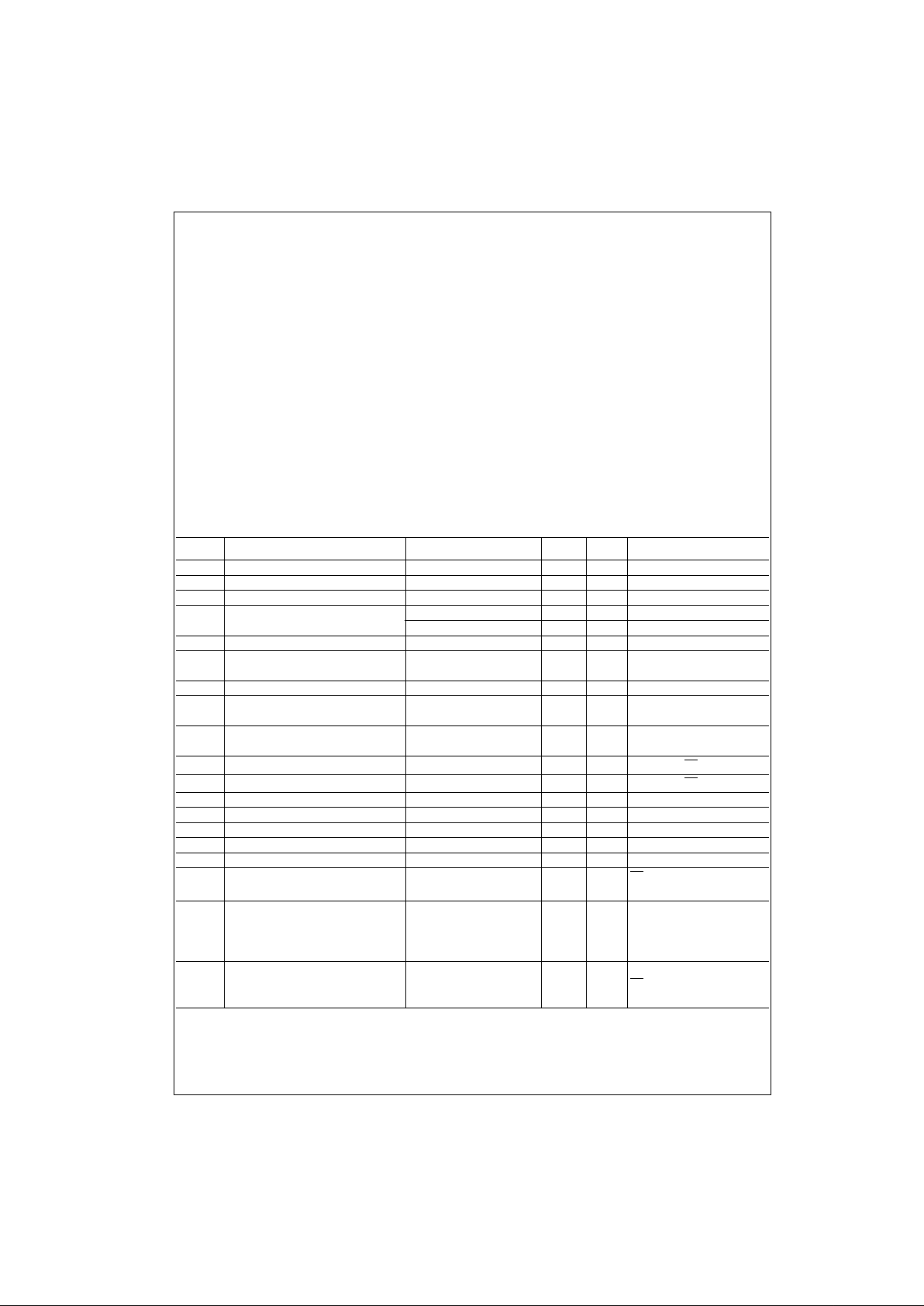
Ordering Code:
Devices also availab le in Tape and Reel. Specify by appending letter suffix “X” to the ordering code.
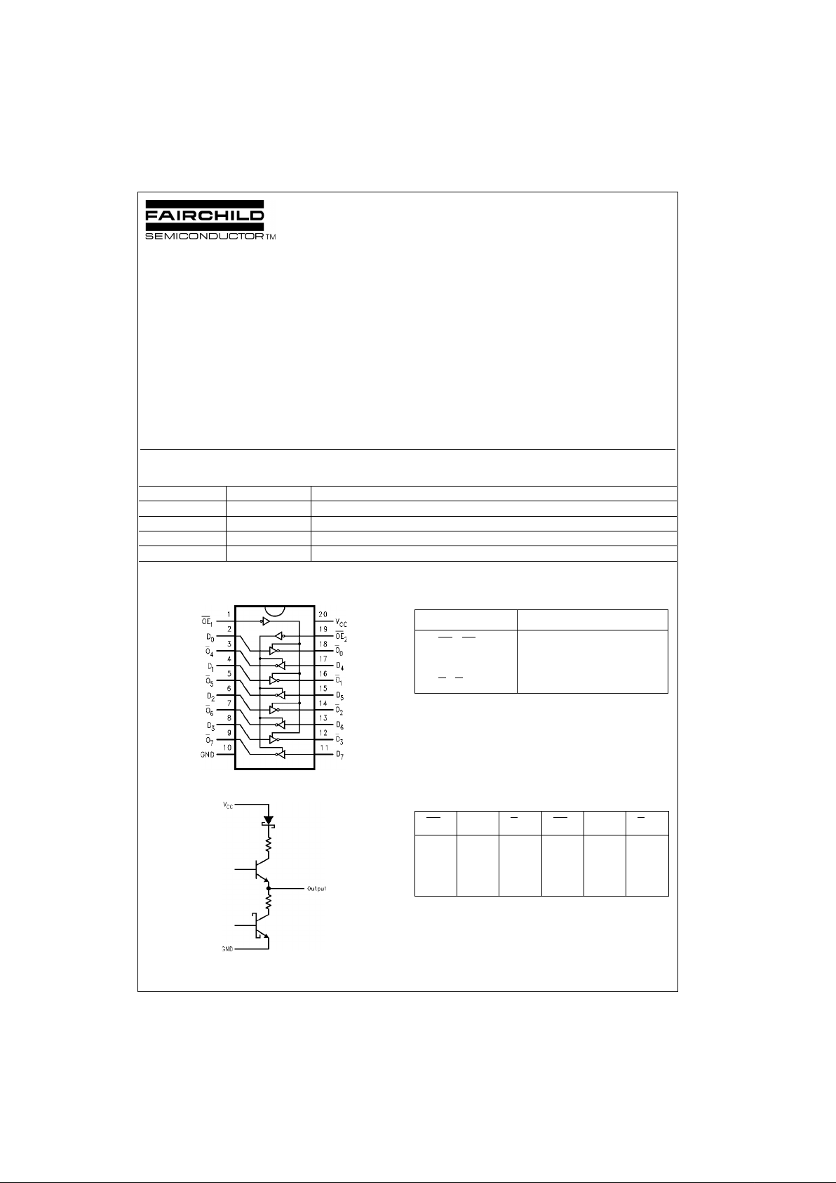
Connection Diagram
Schematic of Each Output
Pin Descriptions
Truth T able
H = HIGH Voltage Level
L = LOW Voltage Level
X = Immaterial
Z = High Impedance
Order Number Package Numb er Package Description
74ABT2240CSC M20B 20-Lead Small Outline Integrated Circuit (SOIC), JEDEC MS-013, 0.300” Wide Body
74ABT2240CSJ M20D 20-Lead Small Outline Package (SOP), EIAJ TYPE II, 5.3mm Wide
74ABT2240CMSA MSA20 20-Lead Shrink Small Outline Package (SSOP), EIAJ TYPE II, 5.3mm Wide
74ABT2240CMTC MTC20 20-Lead Thin Shrink Small Outline Package (TSSOP), JEDEC MO-153, 4.4mm Wide
Pin Names Descriptions
OE
1
, OE
2
Output Enable Input (Active LOW)
D
0–D7
Data Inputs
O
0–O7
Outputs
OE
1
I
0–3
O
0–3
OE
2
I
4–7
O
4–7
H X Z H X Z
L H L L H L
L L H L L H
Page 2
www.fairchildsemi.com 2
74ABT2240
Absolute Maximum Ratings(Note 1) Recommended Operating
Conditions
Note 1: Absolute maximum ratings are values beyond which the device
may be damaged or have its useful life impaired. Functional operation
under these conditi ons is not implied.
Note 2: Either voltage lim it or c urrent limit is sufficient to prot ect inputs.
DC Electrical Characteristics
Note 3: Guaranteed, but not tested.
Note 4: For 8 bits toggling, I
CCD
< 0.8 mA/MHz.
Storage Temperature −65°C to +150°C
Ambient Temperature under Bias −55°C to +125°C
Junction Temperature under Bias −55°C to +150°C
V
CC
Pin Potential to Ground Pin −0.5V to +7.0V
Input Voltage (Note 2) −0.5V to +7.0V
Input Current (Note 2) −30 mA to +5.0 mA
Voltage Applied to Any Output
in the Disabled or
Power-off State −0.5V to 5.5V
in the HIGH State −0.5V to V
CC
Current Applied to Output
in LOW State (Max) twice the rated I
OL
(mA)
DC Latchup Source Current
(Across Comm Operating Range) −300 mA
Over Voltage Latchup (I/O) 10V
Free Air Ambient Temperature −40°C to +85°C
Supply Voltage +4.5V to +5.5V
Minimum Input Edge Rate (∆V/∆t)
Data Input 50 mV/ns
Enable Inpu t 20 mV/ns
Symbol Parameter Min Typ Max Units
V
CC
Conditions
V
IH
Input HIGH Voltage 2.0 V Recognized HIGH Signal
V
IL
Input LOW Voltage 0.8 V Recognized LOW Signal
V
CD
Input Clamp Diode Voltage −1.2 V Min IIN = −18 mA
V
OH
Output HIGH 2.5 V Min IOH = −3 mA
Voltage 2.0 V Min IOH = −32 mA
V
OL
Output LOW Voltage 0.8 V Min IOL = 15 mA
I
IH
Input HIGH Current 1
µAMax
VIN = 2.7V (Note 3)
1V
IN
= V
CC
I
BVI
Input HIGH Current Breakdown Test 7 µAMaxVIN = 7.0V
I
IL
Input LOW Current −1
µAMax
VIN = 0.5V (Note 3)
−1V
IN
= 0.0V
V
ID
Input Leakage Test V 0.0 IID = 1.9 µA
All Other Pins Grounded
I
OZH
Output Leakage Current 10 µA0 − 5.5V
V
OUT
= 2.7V; OEn = 2.0V
I
OZL
Output Leakage Current −10 µA0 − 5.5V
V
OUT
= 0.5V; OEn = 2.0V
I
OS
Output Short-Circuit Current −275 mA Max V
OUT
= 0.0V
I
CEX
Output HIGH Leakage Current 50 µAMaxV
OUT
= V
CC
I
ZZ
Bus Drainage Test 100 µA0.0V
OUT
= 5.5V; All Others GND
I
CCH
Power Supply Current 50 µA Max All Outputs HIGH
I
CCL
Power Supply Current 30 mA Max All Outputs LOW
I
CCZ
Power Supply Current
50 µAMax
OEn = V
CC
All Others at VCCor GND
I
CCT
Additional Outputs Enabled 1.5 mA VI = V
CC
− 2.1V
ICC/Input Outputs 3-STATE 1.5 mA Max Enable Input VI = VCC − 2.1V
Outputs 3-STATE 50 µA Data Input VI = VCC − 2.1V
All Others at VCCor GND
I
CCD
Dynamic I
CC
No Load mA/
Max
Outputs OPEN
(Note 3) 0.1
MHz
OEn = GND (Note 4)
One Bit Toggling, 50% Duty Cycle
Page 3
3 www.fairchildsemi.com
74ABT2240
AC Electrical Characteristics
Capacitance
Note 5: C
OUT
is measured at frequency f = 1 MHz, per MIL-STD-883, Method 3012.
Symbol Parameter
T
A
= +25°CT
A
= −40°C to +85°C
Units
V
CC
= +5V VCC = 4.5V–5.5V
C
L
= 50 pF CL = 50 pF
Min Typ Max Min Max
t
PLH
Propagation 1.0 4.9 1.0 4.9
ns
t
PHL
Delay Data to Outputs 1.5 5.3 1.5 5.3
t
PZH
Output Enable 1.5 6.6 1.5 6.6
ns
t
PZL
Time 2.7 6.9 2.7 6.9
t
PHZ
Output Disable 1.9 6.4 1.9 6.4
ns
t
PLZ
Time 1.9 6.4 1.9 6.4
Symbol Parameter Typ Units
Conditions
T
A
= 25°C
C
IN
Input Capacitance 5.0 pF VCC = 0V
C
OUT
(Note 5) Output Capacitance 9.0 pF VCC = 5.0V
Page 4

www.fairchildsemi.com 4
74ABT2240
AC Loading
*Includes jig and pr obe capacitance
FIGURE 1. Standard AC Test Load
FIGURE 2. Propagation Delay,
Pulse Width Waveforms
FIGURE 3. Test Input Signal Requirements
AC Waveforms
FIGURE 4. Propagation Delay Waveforms for
Inverting and Non-Inverting Functions
FIGURE 5. 3-STA TE Output HIGH
and LOW Enable and Disable Times
FIGURE 6. Test Input Signal Levels
FIGURE 7. Setup Time, Hold Time
and Recovery Time Waveforms
Amplitude Rep. Rate t
W
t
r
t
f
3.0V 1 MHz 500 ns 2.5 ns 2.5 ns
Page 5

5 www.fairchildsemi.com
74ABT2240
Physical Dimensions inches (millimeters) unless otherwise noted
20-Lead Small Outline Integrated Circuit (SOIC), JEDEC MS-013, 0.300” Wide Body
Package Number M20B
Page 6

www.fairchildsemi.com 6
74ABT2240
Physical Dimensions inches (millimeters) unless otherwise noted (Continued)
20-Lead Small Outline Package (SOP), EIAJ TYPE II, 5.3mm Wide
Package Number M20D
Page 7

7 www.fairchildsemi.com
74ABT2240
Physical Dimensions inches (millimeters) unless otherwise noted (Continued)
20-Lead Shrink Small Outline Package (SSOP), EIAJ TYPE II, 5.3mm Wide
Package Num b er MSA20
Page 8

www.fairchildsemi.com 8
74ABT2240 Octal Buffer/Line Driver with 25Ω Series Resistors in the Outputs
Physical Dimensions inches (millimeters) unless otherwise noted (Continued)
20-Lead Thin Shrink Small Outline Package (TSSOP), JEDEC MO-153, 4.4mm Wide
Package Number MTC20
Fairchild does not assume any responsibility for use of any circuitr y described, no circuit patent licenses are implied and
Fairchild reserves the right at any time without notice to change said circuitry and specifications.
LIFE SUPPORT POLICY
FAIRCHILD’S PRODUCTS ARE NOT AUTHORIZED FOR USE AS CRITICAL COMPONENTS IN LIFE SUPPORT
DEVICES OR SYSTEMS WITHOUT THE EXPRESS WRITTEN APPROVAL OF THE PRESIDENT OF FAIRCHILD
SEMICONDUCTOR CORPORATION. As used herein:
1. Life support devices or systems are devices or syste ms
which, (a) are intended for surgical implant into the
body, or (b) support or sustain life, and (c) whose failure
to perform when properly used in accordance with
instructions for use provided in the labeling, can be reasonably expected to result in a significant inju ry to the
user.
2. A critical component in any compon ent of a lif e supp ort
device or system whose failure t o perform can be reasonably expected to ca use the failure of the life supp ort
device or system, or to affect its safety or effectiveness.
www.fairchildsemi.com
 Loading...