

Datasheet 74ABT16652CSSCX, 74ABT16652CSSC, 74ABT16652CMTDX, 74ABT16652CMTD Datasheet (Fairchild Semiconductor)
Page 1
April 1993
Revised January 1999
74ABT16652
16-Bit Transceivers and Registers with 3-STATE Outputs
74ABT16652 16-Bit Transceivers and Registers with 3-STATE Outputs
General Description
The ABT16652 consist s of sixteen bus transce iver circuits
with D-type flip-flops, and control circuitry arranged for multiplexed transmission of data directly fro m the input bus or
from the interna l registers. Each byte has separate control
inputs which can be sho rted toge ther for full 16-bit operation. Data on the A or B bus will be clocked into the registers as the appropr iate clock pin goes to HI GH logic level.
Output Enable pins (OEAB, OEBA
the transceiver function.
) are provided to control
Features
■ Independent registers for A and B buses
■ Multiplexed real-time and stored data
■ Separate control logic for each byte
■ A and B output sink capability of 64 mA, source
capability of 32 mA
■ Guaranteed output skew
■ High impedance glitch free bus loading during entire
power up and power down cycle
■ Nondestructive hot insertion capability
Ordering Code:
Order Number Package Number Package Description
74ABT16652CSSC MS56A 56-Lead Shrink Small Outline Package (SSOP), JEDEC MO-118, 0.300” Wide
74ABT16652CMTD MTD56 56-Lead Thin Shrink Small Outline Package (TSSOP), JEDEC MO-153, 6.1mm Wide
Devices also available in Tape and Reel. Specify by appending the suffix letter “X” t o t he ordering code.
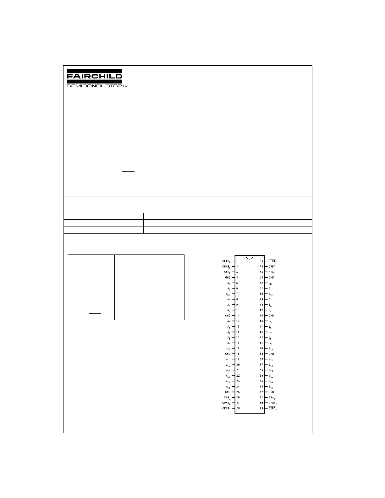
Pin Descriptions Connection Diagram
Pin Names Descriptions
A
0–A16
B
0–B16
CPAB
SAB
OEAB
, CPBA
n
, SBA
n
n
n
, OEBA
Data Register A Inputs/
3-STATE Outputs
Data Register B Inputs/
3-STATE Outputs
Clock Pulse Inputs
n
Select Inputs
Output Enable Inputs
n
© 1999 Fairchild Semiconductor Corporation DS011599.prf www.fairchildsemi.com
Page 2
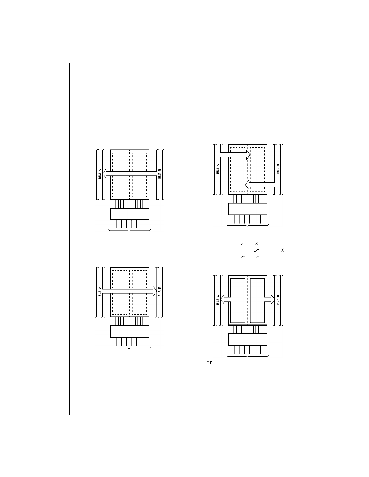
Functional Description
In the transceiver mo de, data presen t at the HI GH impedance port may be stored in either the A or B register or
both.
The select (SAB
real-time.
74ABT16652
The examples in
tal bus-management fun ctions that can be perfor med with
the ABT16652.
, SBAn) controls can multiplex stored and
n
Figure 1
demonstrate the four fundamen -
Data on the A or B data bus, or bot h can be stor ed in the
internal D flip-flop by LOW to HIGH transitions at the
appropriate Clock Inputs (CPAB
, CPBAn) regardless of
n
the Select or Output Enable Inputs. When SAB and SBA
are in the real time transfer mode, it is also possible to
store data without using the internal D flip-flops by simultaneously enabling OE AB
and OEBAn. In this configuration
n
each Output reinforces it s Input. Thu s when a ll other data
sources to the two sets of bus lines are i n a HIGH impedance state, each set of bus lines will remain at its last state.
Note A: Real-Time
Transfer Bus B to Bus A
OEBA1CPAB1CPBA1SAB1SBA
OEAB
1
LLXXXL
Note B: Real-Time
Transfer Bus A to Bus B
Note C: Storage
OEAB1OEBA1CPAB1CPBA1SAB1SBA
1
XH
LXX
LH
XXX
1
XX
XX
Note D: Transfer Storage
Data to A or B
OEBA1CPAB1CPBA1SAB1SBA
OEAB
1
1
HHXXLX
FIGURE 1.
www.fairchildsemi.com 2
OEBA1CPAB1CPBA1SAB1SBA
OEAB
1
H L H or L H or L H H
1
Page 3
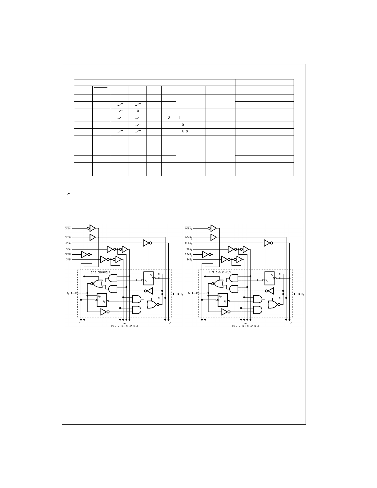
Function Table
Inputs Inputs/Outputs (Note 1) Operating Mode
OEBA1 CPAB1 CPBA1 SAB1 SBA1 A0 thru A7 B0 thru B
OEAB
1
7
L H H or L H or L X X Input Input Isolation
L H
X H
H H
L X H or L
L L
H or L X X Input Not Specified Store A, Hold B
X X Store A and B Data
X X Input Output Store A in Both Registers
X X Not Specified Input Hold A, Store B
X X Output Input Store B in Both Registers
L L X X X L Output Input Real-Time B Data to A Bus
L L X H or L X H Store B Data to A Bus
H H X X L X
H H H or L X H X Stored A Data to B Bus
Input Output
Real-Time A Data to B Bus
H L H or L H or L H H Output Output Stored A Data to B Bus and
Stored B Data to A Bus
H = HIGH Voltage Level
L = LOW Voltage Level
X = Immaterial
= LOW to HIGH Clock Transition
Note 1: The data ou tput fu nctions may be en abled o r disabled by various sign als at OEAB or O EBA
data at the bus pins will be sto red on every LOW to HIGH transit ion on the clock inputs. This also applies to data I/O (A and B: 8–15) and #2 con tr ol pins.
inputs. Data inpu t fun ctions are always e nabled, i.e.,
Logic Diagrams
74ABT16652
Please note that thes e diagrams are provided only for the understanding of lo gic operations and should not be used to estimat e propagation delays.
3 www.fairchildsemi.com
Page 4

Absolute Maximum Ratings(Note 2)
Storage Temperatu re −65°C to +150°C
Ambient Temperature under Bias −55°C to +125°C
Junction Temperature under Bias −55°C to +150°C
Pin Potential to
V
74ABT16652
CC
Ground Pin −0.5V to +7.0V
Input Voltage (Note 3) −0.5V to +7.0V
Input Current (Note 3) −30 mA to +5.0 mA
Voltage Applied to Any Output
in the Disable or Power-Off State −0.5V to +5.5V
in the HIGH State −0.5V to V
Current Applied to Output
in LOW State (Max) twice the rated I
OL
Over Voltage Latchup (I/O) 10V
Recommended Operating
Conditions
Free Air Ambient Temperature −40°C to +85°C
Supply Voltage +4.5V to +5.5V
Minimum Input Edge Rate (∆V/∆t)
Data Input 50 mV/ns
Enable Input 20 mV/ns
Clock Input 100 mV/ns
Note 2: Absolute maxim um ratings are values b eyond which the device
CC
may be damaged or have its useful life impaired. Functional operation
under these conditi ons is not implied.
Note 3: Either voltage limit or current limit is s uf f ic ient to protect inputs.
(mA)
DC Latchup Source Current −500 mA
DC Electrical Characteristics
Symbol Parameter Min Typ Max Units V
V
V
V
V
V
V
I
IH
I
BVI
I
BVIT
I
IL
IIH + I
IIL + I
I
OS
I
CEX
I
ZZ
I
CCH
I
CCL
I
CCZ
I
CCT
I
CCD
Note 4: Guaranteed but not tested.
Input HIGH Voltage V Recognized HIGH Signal
IH
Input LOW Voltage 0.8 V Recognized LOW Signal
IL
Input Clamp Diode Voltage −1.2 V Min IIN = −18 mA (Non I/O Pins)
CD
Output HIGH 2.5 V Min IOH = −3 mA, (An, Bn)
OH
Voltage 2.0 IOH = −32 mA, (An, Bn)
Output LOW Voltage 0.55 V Min IOL = 64 mA, (An, Bn)
OL
Input Leakage Test V 0.0 IID = 1.9 µA, (Non-I/O Pins)
ID
Input HIGH Current 1 µA Max VIN = 2.7V (Non-I/O Pins) (Note 4)
Input HIGH Current 7 µA Max VIN = 7.0V (Non-I/O Pins)
Breakdown Test
Input HIGH Current 100 µA Max VIN = 5.5V (An, Bn)
Breakdown Test (I/O)
Input LOW Current −1 µA Max VIN = 0.5V (Non-I/O Pins) (Note 4)
Output Leakage Current 10 µA 0V–5.5V V
OZH
Output Leakage Current −10 µA 0V–5.5V V
OZL
Output Short-Circuit Current −275 mA Max V
Output HIGH Leakage Current 50 µA Max V
Bus Drainage Test 100 µA 0.0V V
Power Supply Current 1.0 mA Max All Outputs HIGH
Power Supply Current 60 mA Max All Outputs LOW
Power Supply Current 1.0 mA Max Outputs 3-STATE;
Additional ICC/Input 2.5 mA Max VI = VCC − 2.1V
Dynamic I
(Note 4)
CC
No Load 0.23 mA/MHz Max Outputs Open
1 V
−1 V
CC
All Other Pins Grounded
IN
IN
OUT
OEABn = GND and OEBAn = 2.0V
OUT
OEABn = GND and OEBAn = 2.0V
OUT
OUT
OUT
All Others at VCC or GND
All Others at VCC or GND
OEABn, OEBAn and SEL = GND
Non-I/O = GND or V
One bit toggling, 50% duty cycle
Conditions
= VCC (Non-I/O Pins)
= 0.0V (Non-I/O Pins)
= 2.7V (An, Bn);
= 0.5V (An, Bn);
= 0V (An, Bn)
= VCC (An, Bn)
= 5.5V (An, Bn); All Others GND
CC
www.fairchildsemi.com 4
Page 5

DC Electrical Characteristics
(SSOP Package)
Symbol Parameter Min Typ Max Units
V
V
V
V
V
Quiet Output Maximum Dynamic V
OLP
Quiet Output Minimum Dynamic V
OLV
Minimum HIGH Level Dynamic Output Voltage 2.5 3.0 V 5.0 TA = 25° (Note 6)
OHV
Minimum HIGH Level Dynamic Input Voltage 2.0 1.6 V 5.0 TA = 25°C (Note 7)
IHD
Maximum LOW Level Dynamic Input Voltage 1.2 0.8 V 5.0 TA = 25°C (Note 7)
ILD
Note 5: Max number of ou t puts defined as (n). n − 1 data inputs are driven 0V to 3V. One output at LOW. Guaranteed, but not tested.
Note 6: Max number of ou t puts defined as (n). n − 1 data inputs are driven 0V to 3V. One output HIGH. Gua ranteed, but not tested.
Note 7: Max number o f dat a inp uts (n) switchi ng. n − 1 in pu ts switchin g 0 V to 3 V. Input-under-test switchi ng: 3 V to t hres hold (V
Guaranteed, but not tested.
OL
OL
−1.4 −1.0 V 5.0 TA = 25°C (Note 5)
0.7 1.2 V 5.0 TA = 25°C (Note 5)
V
CC
AC Electrical Characteristics
(SSOP Package)
Symbol Parameter
t
PLH
t
PHL
t
PLH
t
PHL
t
PLH
t
PHL
t
PZH
t
PZL
t
PHZ
t
PLZ
Propagation Delay 1.5 3.0 4.9 1.5 4.9 ns
Clock to Bus 1.5 3.4 4.9 1.5 4.9
Propagation Delay 1.5 2.6 4.5 1.5 4.5 ns
Bus to Bus 1.5 3.0 4.5 1.5 4.5
Propagation Delay 1.5 2.9 5.0 1.5 5.0 ns
SBAn or SAB
to An to B
n
n
Enable Time 1.5 2.8 5.5 1.5 5.5 ns
OEBAn or OEAB
to An or B
n
n
Disable Time 1.5 3.9 5.9 1.5 5.9 ns
OEBAn or OEAB
to An or B
n
n
TA = +25°C T
= −40°C to +85°C
A
VCC = +5.0V VCC = 4.5V–5.5V
CL = 50 pF CL = 50 pF
Min Typ Max Min Max
1.5 3.2 5.0 1.5 5.0
1.5 3.0 5.5 1.5 5.5
1.5 3.3 5.9 1.5 5.9
Conditions
CL = 50 pF, RL = 500Ω
), 0V to threshold (V
ILD
IHD
Units
74ABT16652
).
AC Operating Requirements
TA = +25°CT
Symbol Parameter
VCC = +5.0V VCC = 4.5V–5.5V
CL = 50 pF CL = 50 pF
Min Typ Max Min Max
f
max
Max Clock Frequency 200 MHz
tS(H) Setup Time, HIGH 2.0 2.0 ns
tS(L) or LOW Bus to Clock
tH(H) Hold Time, HIGH 1.0 1.0 ns
tH(L) or LOW Bus to Clock
tW(H) Pulse Width, 3.0 3.0 ns
tW(L) HIGH or LOW
5 www.fairchildsemi.com
= −40°C to +85°C
A
Units
Page 6

Extended AC Electr ical Characteristics
(SSOP Package)
Symbol Parameter
74ABT16652
t
PLH
t
PHL
t
PLH
t
PHL
t
PLH
t
PHL
t
PZH
t
PZL
t
PHZ
t
PLZ
Note 8: This specific ation is guaranteed but n ot te s te d. T he limits apply to propag at ion delays for all paths described switching in phase
(i.e., all LOW-to-HIGH, HIGH-to-LOW, etc.).
Note 9: This specific ation is guaranteed but n ot te s te d. T he limits represent pro pagation delay with 250 pF load capacitors in plac e of t he 50 pF load
capacitors in the standard AC load. This spec if ic ation pertains to sin gle output switching only.
Note 10: This spec if ic at ion is guaranteed but not tes t ed. The limits represent propagation delays for all paths described switching in phase
(i.e., all LOW-to-HIGH, HIGH-to-LOW, etc.) with 250 pF load capacitors in place of the 50 pF loa d c apacitors in the stan dard AC load.
Note 11: The 3-STATE delay times are dominated by the RC network (500Ω, 250 pF) on the output and has been excluded fro m th e datasheet.
Progagation Delay 1.5 5.8 2.0 7.5 2.5 10.0 ns
Clock to Bus 1.5 5.8 2.0 7.5 2.5 10.0
Progagation Delay 1.5 6.5 2.0 7.0 2.5 9.5 ns
Bus to Bus 1.5 6.5 2.0 7.0 2.5 9.5
Progagation Delay 1.5 6.0 2.0 7.5 2.5 10.0
SBA or SAB to 1.5 6.0 2.0 7.5 2.5 10.0 ns
An or B
n
Output Enable Time 1.5 6.0 2.0 8.0 2.5 10.5
OEBAn or OEABn to
An or B
n
Output Disable Time 1.5 6.0
OEBA or OEAB to
An or B
n
TA = −40°C to +85°CTA = −40°C to +85°CTA = −40°C to +85°C
VCC = 4.5V–5.5V VCC = 4.5V–5.5V VCC = 4.5V–5.5V
CL = 50 pF CL = 250 pF CL = 250 pF
16 Outputs Switching 1 Output Switching 16 Outputs Switching
(Note 8) (Note 9) (Note 10)
Min Max Min Max Min Max
1.5 6.0 2.0 8.0 2.5 10.5 ns
1.5 6.0 (Note 11) (Note 11) ns
Skew (Note 12)
(SSOP Package)
Symbol Parameter
t
OSHL
(Note 14) HL Transitions
t
OSLH
(Note 14) LH Transitions
t
PS
(Note 15) LH–HL Skew
t
OST
(Note 14) LH/HL Transitions
t
PV
(Note 16) LH/HL Transitions
Note 12: This spec if ic at ion is guaranteed but not tes t ed. The limits apply to pro pagation delays for all paths de s c ribed switching in phase
(i.e., all LOW-to-HIGH, HIGH-to-LOW, etc.).
Note 13: This spe cification is g uaranteed but n ot tested. The l imits represe nt propagation delays with 250 pF load capacitors in place of the 50 pF load
capacitors in the standard AC load.
Note 14: Skew is defined as the ab solute value of t he differenc e bet ween the actua l propag ation d elays for any tw o sepa rate outp uts of the same device.
The specificati on applies to any outputs switching HIG H t o LOW (t
LOW (t
Note 15: This descr ibes the difference bet ween the de lay of the LOW-to-HIGH and the HI GH-to -LOW transition on the sa me pin. It is me asured ac ross all
the outputs (drivers ) on the same chip, the worst (largest delta) number is the guaranteed specif ic at ion. This specification is guaranteed but not test ed.
Note 16: Propagation delay variation for a given set of conditions (i.e., temperature and V
tested.
Pin to Pin Skew 2.0 2.5 ns
Pin to Pin Skew 2.0 2.5 ns
Duty Cycle 2.0 2.5
Pin to Pin Skew 2.8 3.0 ns
Device to Device Skew 3.5 4.0 ns
). This specificatio n is guaranteed but not teste d.
OST
TA = −40°C to +85°CT
= −40°C to +85°C
A
VCC = 4.5V–5.5V VCC = 4.5V–5.5V
CL = 50 pF CL = 250 pF
16 Outputs Switching 16 Outputs Switching
(Note 12) (Note 13)
Max Max
), LOW to HIGH (t
OSHL
), or any combination switching LOW to HI GH and/or HIGH to
OSLH
) from device to device. T his specification is guaranteed but not
CC
Units
Units
www.fairchildsemi.com 6
Page 7

Capacitance
Symbol Parameter Typ Units
C
IN
C
(Note 17) I/O Capacitance 11.0 pF VCC = 5.0V (An, Bn)
I/O
Note 17: C
Input Capacitance 5.0 pF VCC = 0V (non I/O pins)
is measured at frequency, f = 1 MHz, per MIL-STD-883, Method 3012.
I/O
AC Loading
74ABT16652
Conditions
(TA = 25°C)
*Includes jig and prob e c apacitance
FIGURE 2. Standard AC Test Load
Input Pulse Requirement
Amplitude Rep. Rate t
3.0V 1 MHz 500 ns 2.5 ns 2.5 ns
FIGURE 4. Test input Signal Requirements
AC Waveforms
FIGURE 5. Propagation Delay Waveforms for Inverting
and Non-Inverting Functions
FIGURE 3. Test Input Signal Levels
W
t
t
r
f
FIGURE 7. 3-STATE Output HIGH
and LOW Enable and Disable Times
FIGURE 6. Propagation Delay,
Pulse Width Waveforms
FIGURE 8. Setup Time, Hold Time
and Recovery Time Waveforms
7 www.fairchildsemi.com
Page 8

Physical Dimensions in ches (millimeters) unless otherwise noted
74ABT16652
56-Lead Shrink Small Outline Package (SSOP), JEDEC MO-118, 0.300” Wide
Package Number MS56A
www.fairchildsemi.com 8
Page 9

Physical Dimensions inches (millimeters) unless otherwise noted (Continued)
74ABT16652 16-Bit Transceivers and Registers with 3-STATE Outputs
56-Lead Thin Shrink Small Outline Package (TSSOP), JEDEC MO-153, 6.1mm Wide
LIFE SUPPORT POLICY
FAIRCHILD’S PRODUCTS ARE NOT AUTHORIZED FOR USE AS CRITICAL COMPONENTS IN LIFE SUPPORT
DEVICES OR SYSTEMS WITHOUT THE EXPRESS WRITTEN APPROVAL OF THE PRESIDENT OF FAIRCHILD
SEMICONDUCTOR CORPORATION. As used herein:
1. Life support devices or system s a re devices or syste ms
which, (a) are intended for surgical implant into the
body, or (b) support or sustain life, and (c) whose failure
to perform when properly used in accordance with
instructions for use provided in the labeling, can be reasonably expected to result in a significant injur y to the
user.
Fairchild does not assume any responsibility for use of any circuitry described, no circuit patent licenses are implied and Fairchild reserves the right at any time without notice to change said circuitry and specifications.
Package Number MTD56
2. A critical compon ent in any com ponent of a li fe support
device or system whose failure to perform can be reasonably expected to cause the failure of the life suppor t
device or system, or to affect its safety or effectiveness.
www.fairchildsemi.com
 Loading...