

Datasheet 74ABT16543CMTD, 74ABT16543CSSCX, 74ABT16543CSSC, 74ABT16543CMTDX Datasheet (Fairchild Semiconductor)
Page 1
October 1993
Revised January 1999
74ABT16543
16-Bit Registered Transceiver with 3-STATE Outputs
74ABT16543 16-Bit Registered Transceiver with 3-STATE Outputs
General Description
The ABT16543 16-bit trans ceiver contains two sets of Dtype latches for temporar y st orage o f data flowing in either
direction. Separate Latch Enable and Output Enable inputs
are provided for each register to permit indep endent control of inputting and out putting in either direction of data
flow. Each byte has separate control inputs, which can be
shorted together for full 16-bit operation.
Features
■ Back-to-back registers for storage
■ Bidirectional data path
■ A and B outputs have current sourcing capability of 32
mA and current sinking capability of 64 mA
■ Separate control logic for each byte
■ 16-bit version of the ABT543
■ Separate controls for data flow in each direction
■ Guaranteed latchup protection
■ High impedance glitch free bus loading during entire
power up and power down cycle
■ Nondestructive hot insertion capability
Ordering Code:
Order Number Package Number Package Description
74ABT16543CSSC MS56A 56-Lead Shrink Small Outline Package (SSOP), JEDEC MO-118, 0.300” Wide
74ABT16543CMTD MTD56 56-Lead Thin Shrink Small Outline Package (TSSOP), JEDEC MO-153, 6.1mm Wide
Devices also available on Tape and Reel. Specify by appending the suffix letter “X” to the ordering code.
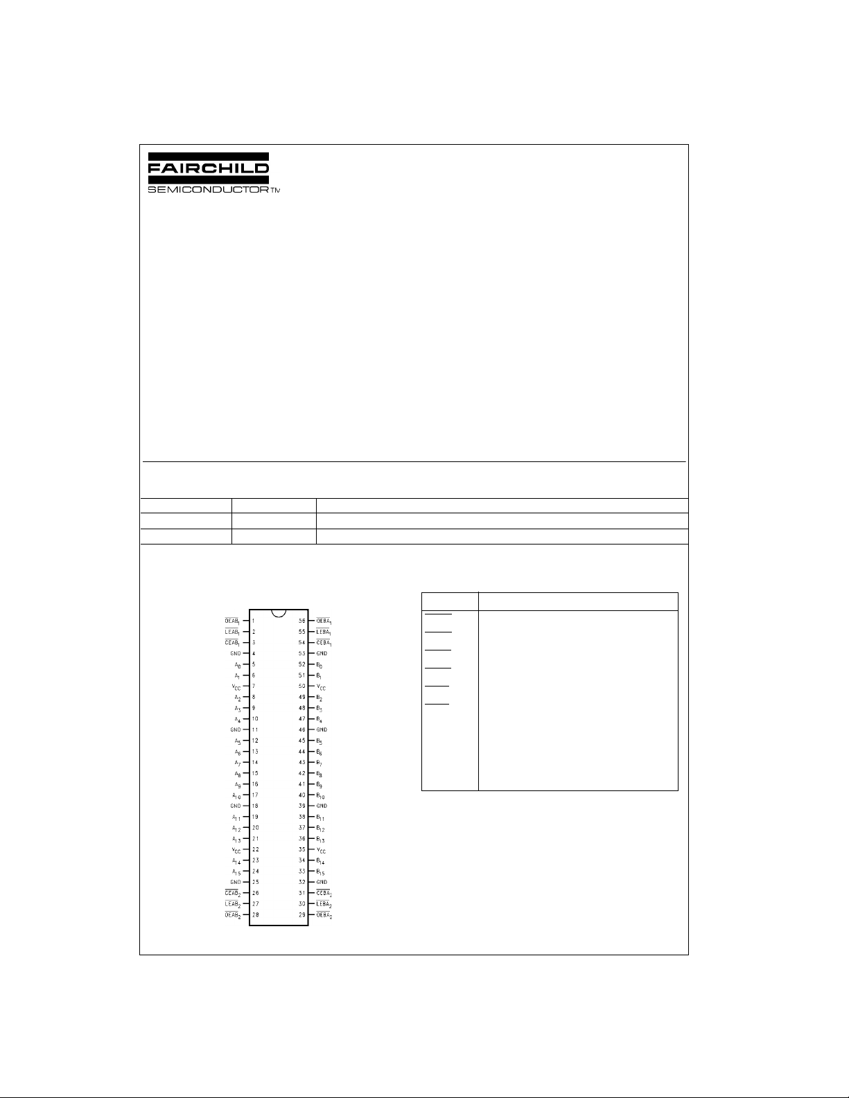
Connection Diagram
Pin Assignment for SSOP and TSSOP
Pin Descriptions
Pin Names Description
OEAB
OEBA
CEAB
CEBA
LEAB
LEBA
A
0–A15
B
0–B15
A-to-B Output Enable Input (Active LOW)
n
B-to-A Output Enable Input (Active LOW)
n
A-to-B Enable Input (Active LOW)
n
B-to-A Enable Input (Active LOW)
n
A-to-B Latch Enable Input (Active LOW)
n
B-to-A Latch Enable Input (Active LOW)
n
A-to-B Data Inputs or
B-to-A 3-STATE Outputs
B-to-A Data Inputs or
A-to-B 3-STATE Outputs
© 1999 Fairchild Semiconductor Corporation DS011646.prf www.fairchildsemi.com
Page 2
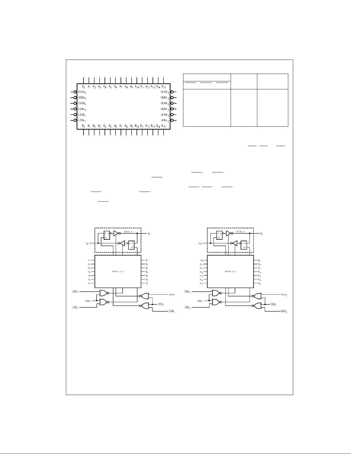
Logic Symbol Data I/O Control Table
Inputs Latch Status Output Buffers
LEABnOEAB
CEAB
74ABT16543
n
H X X Latched HIGH Z
n
X H X Latched —
L L X Transparent —
XXH — HIGH Z
L X L — Driving
H = HIGH Voltage Level
L = LOW Voltage Level
X = Immaterial
A-to-B data flow shown;
B-to-A flow control is the s am e, except us ing CEBA
Functional Description
The ABT16543 con tains two sets of D-type la tches, with
separate input and output control s for each. For data flow
from A to B, for example, the A to B Enable (CEAB
) input
must be low in order to enter data from the A port or take
data from the B-Port as indicated in the Data I/O Contr ol
Table. With CEAB
low, a low signal on (LEAB) input makes
the A to B latches transparent; a su bsequent low to high
transit ion of the LEAB
line puts the A latches in the storage
mode and their outputs no longer change with the A inputs.
With CEAB
and OEAB both low, the B output buffers are
active and reflect the data present on th e output of the A
latches. Control of data flow from B to A is similar, but using
the CEBA
, LEBA and OEBA. Each byte has separate co ntrol inputs, allowing the device to be used as two 8-bit
transceivers or as one 16-bit transceiver.
Logic Diagrams
(Byte n) (Byte n)
, LEBAn and OEBA
n
n
Byte 1 (0:7)
Please note that this diagram is provided only for the understanding of logic
operations and should not be used to estimate propagation delays.
Byte 2 (8:15)
Please note that this diagram is provided only for the understanding of logic
operations and should not be used to estimat e propagation delays.
www.fairchildsemi.com 2
Page 3
Absolute Maximum Ratings(Note 1)
Storage Temperature −65°C to +150°C
Ambient Temperature under Bias −55°C to +125°C
Junction Temperature under Bias −55°C to +150°C
Pin Potential to
V
CC
Ground Pin −0.5V to +7.0V
Input Voltage (Note 2) −0.5V to +7.0V
Input Current (Note 2) −30 mA to +5.0 mA
Voltage Applied to Any Output
in the Disable or
Power-Off State −0.5V to +5.5V
in the HIGH State −0.5V to V
Current Applied to Output
in LOW State (Max) twice the rated I
OL
(mA)
DC Electrical Characteristics
DC Latchup Source Current −500 mA
Over Voltage Latchup (I/O) 10V
Recommended Operating
Conditions
Free Air Ambient Temperature −40°C to +85°C
Supply Voltage +4.5V to +5.5V
Minimum Input Edge Rate (∆V/∆t)
Data Input 50 mV/ns
Enable Input 20 mV/ns
Clock Input 100 mV/ns
Note 1: Absolute maximum ratin gs are values beyond which the device
CC
may be damaged or have its useful life impaired. Functional operation
under these condit ions is not implied.
Note 2: Either voltage limit or current limi t is s uf f ic ient to protect inputs.
74ABT16543
Symbol Parameter Min Typ Max Units
V
V
V
V
V
V
I
I
I
I
IIH + I
IIL + I
I
I
I
I
I
I
I
I
Input HIGH Voltage 2.0 V Recognized HIGH Signal
IH
Input LOW Voltage 0.8 V Recognized LOW Signal
IL
Input Clamp Diode Voltage −1.2 V Min IIN = −18 mA (Non I/O Pins)
CD
Output HIGH Voltage 2.5 IOH = −3 mA, (An, Bn)
OH
Output LOW Voltage 0.55 V Min IOL = 64 mA, (An, Bn)
OL
Input Leakage Test 4.75 V 0.0 IID = 1.9 µA, (Non-I/O Pins)
ID
Input HIGH Current 1 µAMaxVIN = 2.7V (Non-I/O Pins) ((Note 3)
IH
Input HIGH Current Breakdown Test 7 µAMaxVIN = 7.0V (Non-I/O Pins)
BVI
Input HIGH Current 100 µAMaxVIN = 5.5V (An, Bn)
BVIT
Breakdown Test (I/O)
Input LOW Current −1 µAMaxVIN = 0.5V (Non-I/O Pins) (Note 3)
IL
Output Leakage Current 10 µA 0V–5.5V V
OZH
Output Leakage Current −10 µA 0V–5.5V V
OZL
Output Short-Circuit Current −100 −275 mA Max V
OS
Output HIGH Leakage Current 50 µAMaxV
CEX
Bus Drainage Test 100 µA0.0VV
ZZ
Power Supply Current 1.0 mA Max All Outputs HIGH
CCH
Power Supply Current 60 mA Max All Outputs LOW
CCL
Power Supply Current 1.0 mA Max Outputs 3-STATE
CCZ
Additional ICC/Input 2.5 mA Max VI = VCC − 2.1V
CCT
Dynamic I
CCD
Note 3: Guaranteed but not tested.
CC
(Note 3) 0.25 mA/MHz Max
No Load
2.0 IOH = −32 mA, (An, Bn)
1V
−1V
V
CC
All Other Pins Grounded
= VCC (Non-I/O Pins)
IN
= 0.0V (Non-I/O Pins)
IN
OUT
OEAB or CEAB = 2V
OUT
OEAB or CEAB = 2V
OUT
OUT
OUT
All Others at VCC or GND
All Others at VCC or GND
Outputs Open, CEAB, OEAB, LEAB = GND,
CEBA = VCC, One Bit Toggling,
50% Duty Cycle
Conditions
= 2.7V (An, Bn);
= 0.5V (An, Bn);
= 0V (An, Bn)
= VCC (An, Bn)
= 5.5V (An, Bn); All Others GND
3 www.fairchildsemi.com
Page 4

AC Electrical Charac teristics
Symbol Parameter
74ABT16543
t
PLH
t
PHL
t
PLH
t
PHL
t
PZH
t
PZL
t
PHZ
t
PLZ
t
PZH
t
PZL
t
PHZ
t
PLZ
Propagation Delay 1.5 3.0 5.7 1.5 5.7 ns
An to Bn or Bn to A
Propagation Delay 1.5 3.0 5.5 1.5 5.5 ns
LEABn to Bn, LEBAn to A
Enable Time 1.5 2.8 5.2 1.5 5.2 ns
OEBAn or OEABn to An or B
Disable Time 1.6 3.1 6.0 1.6 6.0 ns
OEABn or OEBAn to An or B
Enable Time 1.5 3.1 6.2 1.5 6.2 ns
CEBAn or CEABn to An or B
Disable Time 1.7 3.2 6.3 1.7 6.3 ns
CEBAn or CEABn to An or B
TA = +25°CT
VCC = +5.0V VCC = 4.5V–5.5V
CL = 50 pF CL = 50 pF
Min Typ Max Min Max
n
n
n
n
n
n
= −55°C to +85°C
A
AC Operating Requirements
(SSOP Package)
Symbol Parameter
tS(H) Setup Time, HIGH or LOW 2.0 2.0 ns
tS(L)
An or Bn to LEBAn or LEAB
n
tH(H) Hold Time, HIGH or LOW 1.0 1.0 ns
tH(L)
An or Bn to LEBAn or LEAB
n
tW(L) Pulse Width, LOW 3.0 3.0 ns
TA = +25°CT
= −55°C to +85°C
A
VCC = +5.0V VCC = 4.5V–5.5V
CL = 50 pF CL = 50 pF
Min Max Min Max
2.0 2.0
1.0 1.0
Units
Units
Capacitance
Symbol Parameter Typ Units
C
IN
C
(Note 4) Output Capacitance 11.0 pF VCC = 5.0V (An, Bn)
I/O
Note 4: C
www.fairchildsemi.com 4
Input Capacitance 5.0 pF VCC = 0V (non I/O pins)
is measured at frequency, f = 1 MHz, per MIL-STD-883, Method 3012.
I/O
Conditions
TA = 25°C
Page 5

AC Loading
74ABT16543
*Includes jig and prob e c apacitance
FIGURE 1. Standard AC Test Load
Amplitude Rep. Rate t
AC Waveforms
FIGURE 4. Propagation Delay Waveforms
for Inverting and Non-Inverting Functions
FIGURE 2. V
Input Pulse Requirement s
W
3V 1 MHz 500 ns 2.5 ns 2.5 ns
FIGURE 3. Test Input Signal Requirements
t
FIGURE 6. 3-STATE Output HIGH
and LOW Enable and Disable Times
t
r
f
= 1.5V
M
FIGURE 5. Propagation Delay,
Pulse Width Waveforms
FIGURE 7. Setup Time, Hold Time
and Recovery Time Waveforms
5 www.fairchildsemi.com
Page 6

Physical Dimensions in ches (millimeters) unless otherwise noted
74ABT16543
56-Lead Shrink Small Outline Package (SSOP), JEDEC MO-118, 0.300” Wide
Package Number MS56A
www.fairchildsemi.com 6
Page 7

Physical Dimensions inches (millimeters) unless otherwise noted (Continued)
74ABT16543 16-Bit Registered Transceiver with 3-STATE Outputs
56-Lead Thin Shrink Small Outline Package (TSSOP), JEDEC MO-153, 6.1mm Wide
LIFE SUPPORT POLICY
FAIRCHILD’S PRODUCTS ARE NOT AUTHORIZED FOR USE AS CRITICAL COMPONENTS IN LIFE SUPPORT
DEVICES OR SYSTEMS WITHOUT THE EXPRESS WRITTEN APPROVAL OF THE PRESIDENT OF FAIRCHILD
SEMICONDUCTOR CORPORATION. As used herein:
1. Life support devices or systems a re devices or syste ms
which, (a) are intended for surgical implant into the
body, or (b) support or sustain life, and (c) whose failure
to perform when properly used in accordance with
instructions for use provided in the labeling, can be reasonably expected to result in a significant injur y to the
user.
Fairchild does not assume any responsibility for use of any circuitry described, no circuit patent licenses are implied and Fairchild reserves the right at any time without notice to change said circuitry and specifications.
Package Number MTD56
2. A critical compon ent in a ny compon ent of a life suppo r t
device or system whose failure to perform can be reasonably expected to cause the failure of the life suppor t
device or system, or to affect its safety or effectiveness.
www.fairchildsemi.com
 Loading...