

Datasheet AD637SQ-883B, AD637SD-883B, AD637SD, AD637SCHIPS, AD637KR Datasheet (Analog Devices)
...Page 1
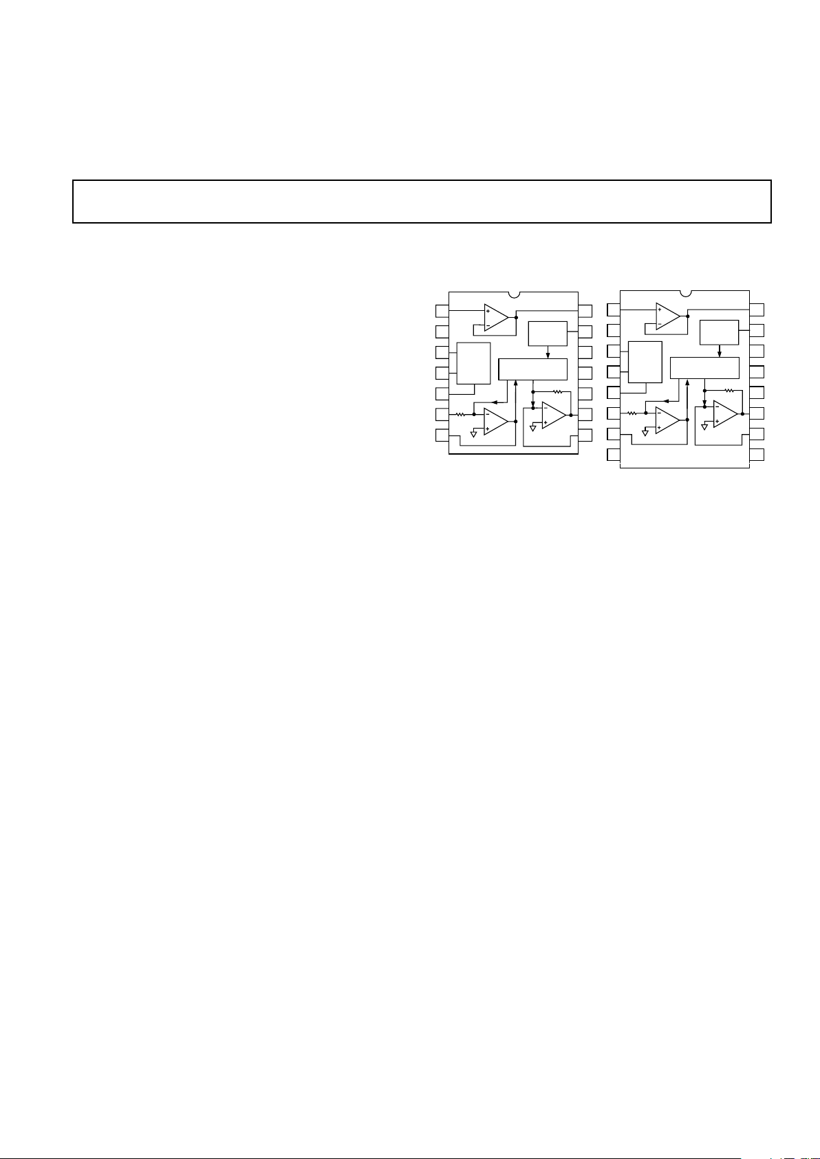
FUNCTIONAL BLOCK DIAGRAMS
REV. F
Information furnished by Analog Devices is believed to be accurate and
reliable. However, no responsibility is assumed by Analog Devices for its
use, nor for any infringements of patents or other rights of third parties that
may result from its use. No license is granted by implication or otherwise
under any patent or patent rights of Analog Devices.
a
High Precision, Wideband
RMS-to-DC Converter
AD637
The AD637 is available in two accuracy grades (J and K) for
commercial (0°C to 70°C) temperature range applications;
two accuracy grades (A and B) for industrial (–40°C to +85°C)
applications; and one (S) rated over the –55°C to +125°C temperature range. All versions are available in hermetically sealed,
14-lead side brazed ceramic DIPs as well as low cost cerdip
packages. A 16-lead SOIC package is also available.
PRODUCT HIGHLIGHTS
1. The AD637 computes the true root-mean-square, meansquare, or absolute value of any complex ac (or ac plus dc)
input waveform and gives an equivalent dc output voltage.
The true rms value of a waveform is more useful than an
average rectified signal since it relates directly to the power of
the signal. The rms value of a statistical signal is also related
to the standard deviation of the signal.
2. The AD637 is laser wafer trimmed to achieve rated
performance without external trimming. The only external
component required is a capacitor that sets the averaging
time period. The value of this capacitor also determines
low-frequency accuracy, ripple level, and settling time.
3. The chip select feature of the AD637 permits the user to
power down the device during periods of nonuse, thereby
decreasing battery drain in remote or hand-held applications.
4. The on-chip buffer amplifier can be used either as an input
buffer or in an active filter configuration. The filter can be
used to reduce the amount of ac ripple, thereby increasing
the accuracy of the measurement.
PRODUCT DESCRIPTION
The AD637 is a complete high accuracy monolithic rms-to-dc
converter that computes the true rms value of any complex waveform. It offers performance that is unprecedented in integrated
circuit rms-to-dc converters and comparable to discrete and
modular techniques in accuracy, bandwidth, and dynamic range.
A crest factor compensation scheme in the AD637 permits measurements of signals with crest factors of up to 10 with less than
1% additional error. The circuit’s wide bandwidth permits the
measurement of signals up to 600 kHz with inputs of 200 mV
rms and up to 8 MHz when the input levels are above 1 V rms.
As with previous monolithic rms converters from Analog Devices,
the AD637 has an auxiliary dB output available to the user. The
logarithm of the rms output signal is brought out to a separate
pin, allowing direct dB measurement with a useful range of
60 dB. An externally programmed reference current allows the
user to select the 0 dB reference voltage to correspond to any
level between 0.1 V and 2.0 V rms.
A chip select connection on the AD637 permits the user to decrease the supply current from 2.2 mA to 350 µA during periods
when the rms function is not in use. This feature facilitates the
addition of precision rms measurement to remote or hand-held
applications where minimum power consumption is critical. In
addition when the AD637 is powered down the output goes to a
high impedance state. This allows several AD637s to be tied
together to form a wideband true rms multiplexer.
The input circuitry of the AD637 is protected from overload
voltages that are in excess of the supply levels. The inputs will
not be damaged by input signals if the supply voltages are lost.
FEATURES
High Accuracy
0.02% Max Nonlinearity, 0 V to 2 V RMS Input
0.10% Additional Error to Crest Factor of 3
Wide Bandwidth
8 MHz at 2 V RMS Input
600 kHz at 100 mV RMS
Computes:
True RMS
Square
Mean Square
Absolute Value
dB Output (60 dB Range)
Chip Select/Power-Down Feature Allows:
Analog “Three-State” Operation
Quiescent Current Reduction from 2.2 mA to 350 A
Side Brazed DIP, Low Cost Cerdip and SOIC
One Technology Way, P.O. Box 9106, Norwood, MA 02062-9106, U.S.A.
Tel: 781/329-4700 www.analog.com
Fax: 781/326-8703 © Analog Devices, Inc., 2002
BUFFER
AD637
ABSOLUTE
VALUE
SQUARER/DIVIDER
BIAS
SECTION
FILTER
25k
25k
1
2
3
4
5
6
7
14
13
12
11
10
98
16
15
SOIC (R) Package
BUFFER
AD637
ABSOLUTE
VALUE
SQUARER/DIVIDER
BIAS
SECTION
FILTER
25k
25k
1
2
3
4
5
6
7
14
13
12
11
10
9
8
Ceramic DIP (D) and
Cerdip (Q) Packages
Page 2

AD637J/A AD637K/B AD637S
Model Min Typ Max Min Typ Max Min Typ Max Unit
TRANSFER FUNCTION
V avg V
OUT IN
=×
()
2
V avg V
OUT IN
=×
()
2
V avg V
OUT IN
=×
()
2
CONVERSION ACCURACY
Total Error, Internal Trim
1
(Fig. 2)
1
0.5
0.5 0.2
1
0.5 mV ± % of Reading
T
MIN
to T
MAX
3.0 0.6
2.0 0.3
6
0.7 mV ± % of Reading
vs. Supply, + V
IN
= +300 mV 30 150 30 150 30 150 µV/V
vs. Supply, – V
IN
= –300 mV 100 300 100 300 100 300 µV/V
DC Reversal Error at 2 V 0.25 0.1 0.25 % of Reading
Nonlinearity 2 V Full Scale
2
0.04 0.02 0.04 % of FSR
Nonlinearity 7 V Full Scale 0.05 0.05 0.05 % of FSR
Total Error, External Trim ±0.5 ± 0.1 ±0.25 ± 0.05 ±0.5 ± 0.1 mV ± % of Reading
ERROR VS. CREST FACTOR
3
Crest Factor 1 to 2 Specified Accuracy Specified Accuracy Specified Accuracy
Crest Factor = 3 ±0.1 ±0.1 ±0.1 % of Reading
Crest Factor = 10 ± 1.0 ±1.0 ± 1.0 % of Reading
AVERAGING TIME CONSTANT 25 25 25 ms/µF C
AV
INPUT CHARACTERISTICS
Signal Range, ±15 V Supply
Continuous RMS Level 0 to 7 0 to 7 0 to 7 V rms
Peak Transient Input ±15 ±15 ±15 V p-p
Signal Range, ±5 V Supply
Continuous rms Level 0 to 4 0 to 4 0 to 4 V rms
Peak Transient Input ±6 ±6 ±6 V p-p
Maximum Continuous Nondestructive
Input Level (All Supply Voltages) ±15 ±15 ±15 V p-p
Input Resistance 6.4 8 9.6 6.4 8 9.6 6.4 8 9.6 kΩ
Input Offset Voltage ±0.5 ± 0.2 ±0.5 mV
FREQUENCY RESPONSE
4
Bandwidth for 1% Additional Error (0.09 dB)
V
IN
= 20 mV 11 11 11 kHz
V
IN
= 200 mV 66 66 66 kHz
V
IN
= 2 V 200 200 200 kHz
±3 dB Bandwidth
V
IN
= 20 mV 150 150 150 kHz
V
IN
= 200 mV 1 1 1 MHz
VIN = 2 V 8 8 8 MHz
OUTPUT CHARACTERISTICS
Offset Voltage
1
0.5
1 mV
vs. Temperature ±0.05
0.089 ±0.04
0.056 ±0.040.07 mV/°C
Voltage Swing, ±15 V Supply,
2 kΩ Load 0 to 12.0 13.5 0 to 12.0 13.5 0 to 12.0 13.5 V
Voltage Swing, ±3 V Supply,
2 kΩ Load 0 to 2 2.2 0 to 2 2.2 0 to 2 2.2 V
Output Current 66 6mA
Short Circuit Current 20 20 20 mA
Resistance, Chip Select “High” 0.5 0.5 0.5 Ω
Resistance, Chip Select “Low” 100 100 100 kΩ
dB OUTPUT
Error, V
IN
7 mV to 7 V rms, ±0.5 ± 0.3 ±0.5 dB
0 dB = 1 V rms
Scale Factor –3 –3 –3 mV/dB
Scale Factor Temperature Coefficient +0.33 +0.33 +0.33 % of Reading/°C
–0.033 –0.033 –0.033 dB/°C
I
REF
for 0 dB = 1 V rms 5 20 80 52080 52080 µA
I
REF
Range 1 100 1 100 1 100 µA
BUFFER AMPLIFIER
Input Output Voltage Range –V
S
to (+VS – 2.5 V) –VS to (+VS – 2.5 V) –VS to (+VS – 2.5 V) V
Input Offset Voltage ±0.8
2 ± 0.5
1 ± 0.82 mV
Input Current ± 2
10 ± 2
5 ± 2
10 nA
Input Resistance 10
8
10
8
10
8
Ω
Output Current (+5 mA, –130 µA) (+5 mA, –130 µA) (+5 mA, –130 µA)
Short Circuit Current 20 20 20 mA
Small Signal Bandwidth 1 1 1 MHz
Slew Rate
5
55 5V/µs
DENOMINATOR INPUT
Input Range 0 to 10 0 to 10 0 to 10 V
Input Resistance 20 25 30 20 25 30 20 25 30 kΩ
Offset Voltage ±0.2 ±0.5 ±0.2 ± 0.5 ±0.2 ±0.5 mV
AD637–SPECIFICATIONS
(@ 25C, and 15 V dc unless otherwise noted.)
REV. F
–2–
Page 3

AD637
REV. F
–3–
AD637J/A AD637K/B AD637S
Model Min Typ Max Min Typ Max Min Typ Max Unit
CHIP SELECT PROVISION (CS)
RMS “ON” Level Open or 2.4 V < V
C
< +V
S
Open or 2.4 V < VC < +V
S
Open or 2.4 V < VC < +V
S
RMS “OFF” Level VC < 0.2 V VC < 0.2 V VC < 0.2 V
I
OUT
of Chip Select
CS “Low” 10 10 10 µA
CS “High” Zero Zero Zero
On Time Constant 10 µs + ((25 kΩ) ⫻ C
AV
) 10 µs + ((25 kΩ) ⫻ CAV) 10 µs + ((25 kΩ) ⫻ CAV)
Off Time Constant 10 µs + ((25 kΩ) ⫻ CAV) 10 µs + ((25 kΩ) ⫻ CAV) 10 µs + ((25 kΩ) ⫻ CAV)
POWER SUPPLY
Operating Voltage Range ±3.0
18
3.0
18
3.0
18 V
Quiescent Current 2.2 3 2.2 3 2.2 3 mA
Standby Current 350 450 350 450 350 450 µA
TRANSISTOR COUNT 107 107 107
NOTES
1
Accuracy specified 0–7 V rms dc with AD637 connected as shown in Figure 2.
2
Nonlinearity is defined as the maximum deviation from the straight line connecting the readings at 10 mV and 2 V.
3
Error vs. crest factor is specified as additional error for 1 V rms.
4
Input voltages are expressed in volts rms. % are in % of reading.
5
With external 2 kΩ pull-down resistor tied to –VS.
Specifications shown in bold are tested on all production units at final electrical test. Results from those tests are used to calculate outgoing quality levels. All min and max specifications
are guaranteed, although only those shown in boldface are tested on all production units.
Specifications subject to change without notice.
Page 4
ABSOLUTE MAXIMUM RATINGS
ESD Rating . . . . . . . . . . . . . . . . . . . . . . . . . . . . . . . . . . 500 V
Supply Voltage . . . . . . . . . . . . . . . . . . . . . . . . . . . . . . ±18 V dc
Internal Quiescent Power Dissipation . . . . . . . . . . . . 108 mW
Output Short Circuit Duration . . . . . . . . . . . . . . . . . Indefinite
Storage Temperature Range . . . . . . . . . . . . –65°C to +150°C
Lead Temperature Range (Soldering 10 secs) . . . . . . . . 300°C
Rated Operating Temperature Range
AD637J, K . . . . . . . . . . . . . . . . . . . . . . . . . . . . 0°C to 70°C
AD637A, B . . . . . . . . . . . . . . . . . . . . . . . . –40°C to +85°C
AD637S, 5962-8963701CA . . . . . . . . . . . –55°C to +125°C
ORDERING GUIDE
Temperature Package Package
Model Range Description Option
AD637AR –40°C to +85°C SOIC R-16
AD637BR –40°C to +85°C SOIC R-16
AD637AQ – 40°C to +85°C Cerdip Q-14
AD637BQ – 40°C to +85°C Cerdip Q-14
AD637JD 0°C to 70°C Side Brazed Ceramic DIP D-14
AD637JD/+ 0°C to 70°C Side Brazed Ceramic DIP D-14
AD637KD 0°C to 70°C Side Brazed Ceramic DIP D-14
AD637KD/+ 0°C to 70°C Side Brazed Ceramic DIP D-14
AD637JQ 0°C to 70°C Cerdip Q-14
AD637KQ 0°C to 70°C Cerdip Q-14
AD637JR 0°C to 70°C SOIC R-16
AD637JR-REEL 0°C to 70°C SOIC R-16
AD637JR-REEL7 0°C to 70°C SOIC R-16
AD637KR 0°C to 70°C SOIC R-16
AD637SD –55°C to +125°C Side Brazed Ceramic DIP D-14
AD637SD/883B –55°C to +125°C Side Brazed Ceramic DIP D-14
AD637SQ/883B –55°C to +125°C Cerdip Q-14
AD637SCHIPS –55°C to +125°CDie
5962-8963701CA* –55°C to +125°C Cerdip Q-14
*A standard microcircuit drawing is available.
FILTER/AMPLIFIER
24k
24k
ONE QUADRANT
SQUARER/DIVIDER
BUFFER
AMPLIFIER
Q1
Q2
Q3
Q4
125
6k
6k
12k
24k
A5
A1
A2
ABSOLUTE VALUE VOLTAGE –
CURRENT CONVERTER
I
1
I
3
I
4
A4
A3
BIAS
Q5
CAV
+V
S
RMS
OUT
COM
CS
DEN
INPUT
OUTPUT
OFFSET
dB
OUT
AD637
V
IN
BUFF OUT
BUFF IN
–V
S
Figure 1. Simplified Schematic
CAUTION
ESD (electrostatic discharge) sensitive device. Electrostatic charges as high as 4000 V readily
accumulate on the human body and test equipment and can discharge without detection.
Although the AD637 features proprietary ESD protection circuitry, permanent damage may
occur on devices subjected to high energy electrostatic discharges. Therefore, proper ESD
precautions are recommended to avoid performance degradation or loss of functionality.
AD637
REV. F
–4–
WARNING!
ESD SENSITIVE DEVICE
Page 5
REV. F
–5–
AD637
PIN CONFIGURATIONS
14-Lead DIP
TOP VIEW
(Not to Scale)
14
13
12
11
10
9
8
1
2
3
4
5
6
7
NC = NO CONNECT
BUFF IN
NC
COMMON
OUTPUT OFFSET
CS
DEN INPUT
dB OUTPUT
BUFF OUT
V
IN
NC
+V
S
–V
S
RMS OUT
C
AV
AD637
16-Lead SOIC
TOP VIEW
(Not to Scale)
16
15
14
13
12
11
10
9
1
2
3
4
5
6
7
8
NC = NO CONNECT
BUFF IN
NC
COMMON
OUTPUT OFFSET
CS
DEN INPUT
dB OUTPUT
NC
BUFF OUT
V
IN
NC
+V
S
–V
S
RMS OUT
C
AV
NC
AD637
14-Lead DIP
Pin No. Mnemonic Description
1 BUFF IN Buffer Input
2, 12 NC No Connection
3 COMMON Analog Common
4 OUTPUT OFFSET Output Offset
5 CS Chip Select
6 DEN INPUT Denominator Input
7 dB OUTPUT dB Output
8C
AV
Averaging Capacitor
Connection
9 RMS OUT rms Output
10 –V
S
Negative Supply
Rail
11 +V
S
Positive Supply Rail
13 V
IN
Signal Input
14 BUFF OUT Buffer Output
PIN FUNCTION DESCRIPTIONS
16-Lead SOIC
Pin No. Mnemonic Description
1 BUFF IN Buffer Input
2, 8, 9, 14 NC No Connection
3 COMMON Analog Common
4 OUTPUT OFFSET Output Offset
5 CS Chip Select
6 DEN INPUT Denominator Input
7 dB OUTPUT dB Output
10 C
AV
Averaging Capacitor
Connection
11 RMS OUT rms Output
12 –V
S
Negative Supply
Rail
13 +V
S
Positive Supply Rail
15 V
IN
Signal Input
16 BUFF OUT Buffer Output
Page 6

AD637
REV. F
–6–
STANDARD CONNECTION
The AD637 is simple to connect for a majority of rms measurements. In the standard rms connection shown in Figure 2, only a
single external capacitor is required to set the averaging time
constant. In this configuration, the AD637 will compute the true
rms of any input signal. An averaging error, the magnitude of
which will be dependent on the value of the averaging capacitor,
will be present at low frequencies. For example, if the filter
capacitor, C
AV
, is 4 µF, this error will be 0.1% at 10 Hz and
increases to 1% at 3 Hz. If it is desired to measure only ac
signals, the AD637 can be ac coupled through the addition of a
nonpolar capacitor in series with the input as shown in Figure 2.
BUFFER
AD637
ABSOLUTE
VALUE
SQUARER/DIVIDER
BIAS
SECTION
FILTER
25k
25k
1
2
3
4
5
6
7
14
13
12
11
10
9
8
C
AV
–V
S
+V
S
NC
V
IN
NC
OPTIONAL
AC COUPLING
CAPACITOR
V
O
=
VIN2
NC = NO CONNECT
Figure 2. Standard RMS Connection
The performance of the AD637 is tolerant of minor variations in
the power supply voltages; however, if the supplies being used
exhibit a considerable amount of high frequency ripple it is
advisable to bypass both supplies to ground through a 0.1 µF
ceramic disc capacitor placed as close to the device as possible.
The output signal range of the AD637 is a function of the supply voltages, as shown in Figure 3. The output signal can be
used buffered or nonbuffered depending on the characteristics
of the load. If no buffer is needed, tie the buffer input (Pin 1) to
common. The output of the AD637 is capable of driving 5 mA
into a 2 kΩ load without degrading the accuracy of the device.
SUPPLY VOLTAGE – DUAL SUPPLY – V
20
15
0
0 185
MAX V
OUT
– Volts 2k Load
10
10
5
153
Figure 3. AD637 Max V
OUT
vs. Supply Voltage
FUNCTIONAL DESCRIPTION
The AD637 embodies an implicit solution of the rms equation
that overcomes the inherent limitations of straightforward rms
computation. The actual computation performed by the AD637
follows the equation
V rms Avg
V
V rms
IN
=
2
Figure 1 is a simplified schematic of the AD637, subdivided
into four major sections: absolute value circuit (active rectifier), square/divider, filter circuit, and buffer amplifier. The
input voltage V
IN
, which can be ac or dc, is converted to a
unipolar current I1 by the active rectifier A1, A2. I1 drives one
input of the squarer/divider, which has the transfer function
I
I
I
4
1
2
3
=
The output current of the squarer/divider I4 drives A4, which
forms a low-pass filter with the external averaging capacitor. If the
RC time constant of the filter is much greater than the longest
period of the input signal, then A4’s output will be proportional
to the average of I4. The output of this filter amplifier is used by
A3 to provide the denominator current I3, which equals Avg. I4
and is returned to the squarer/divider to complete the implicit
rms computation
I Avg
I
I
I rms
4
1
2
4
1
=
=
and
V
OUT
= VIN rms
If the averaging capacitor is omitted, the AD637 will compute the
absolute value of the input signal. A nominal 5 pF capacitor should
be used to ensure stability. The circuit operates identically to that
of the rms configuration except that I3 is now equal to I4, giving
I
I
I
II
4
1
2
4
41
=
=
The denominator current can also be supplied externally by providing a reference voltage, V
REF
, to Pin 6. The circuit operates
identically to the rms case except that I3 is now proportional to
V
REF
. Thus:
I Avg
I
I
4
1
2
3
=
and
V
V
V
O
IN
DEN
=
2
This is the mean square of the input signal.
Page 7

REV. F
–7–
AD637
CHIP SELECT
The AD637 includes a chip select feature that allows the user to
decrease the quiescent current of the device from 2.2 mA to
350 µA. This is done by driving the CS, Pin 5, to below 0.2 V dc.
Under these conditions, the output will go into a high impedance
state. In addition to lowering power consumption, this feature
permits bussing the outputs of a number of AD637s to form a
wide bandwidth rms multiplexer. If the chip select is not being
used, Pin 5 should be tied high.
OPTIONAL TRIMS FOR HIGH ACCURACY
The AD637 includes provisions to allow the user to trim out
both output offset and scale factor errors. These trims will result
in significant reduction in the maximum total error as shown in
Figure 4. This remaining error is due to a nontrimmable input
offset in the absolute value circuit and the irreducible
nonlinearity of the device.
The trimming procedure on the AD637 is as follows:
l. Ground the input signal, V
IN
, and adjust R1 to give 0 V
output from Pin 9. Alternatively R1 can be adjusted to give
the correct output with the lowest expected value of V
IN
.
2. Connect the desired full-scale input to V
IN
, using either a dc
or a calibrated ac signal, and trim R3 to give the correct output at Pin 9, i.e., 1 V dc should give l.000 V dc output. Of
course, a 2 V peak-to-peak sine wave should give 0.707 V dc
output. Remaining errors are due to the nonlinearity.
INPUT LEVEL – V
5.0
2.5
5.0
0 2.00.5
ERROR – mV
1.0
0
2.5
1.5
AD637K MAX
INTERNAL TRIM
AD637K
EXTERNAL TRIM
AD637K: 0.5mV 0.2%
0.25mV 0.05%
EXTERNAL
Figure 4. Max Total Error vs. Input Level AD637K
Internal and External Trims
BUFFER
AD637
SQUARER/DIVIDER
BIAS
SECTION
FILTER
25k
25k
1
2
3
4
5
6
7
14
13
12
11
10
9
8
C
AV
–V
S
+V
S
V rms
OUT
R4
147
+
R3
1k
SCALE FACTOR ADJUST, 2%
R2
1M
R1
50k
–V
S
+V
S
V
IN
OUTPUT
OFFSET
ADJUST
ABSOLUTE
VALUE
Figure 5. Optional External Gain and Offset Trims
CHOOSING THE AVERAGING TIME CONSTANT
The AD637 will compute the true rms value of both dc and ac
input signals. At dc the output will track the absolute value of the
input exactly; with ac signals the AD637’s output will approach the
true rms value of the input. The deviation from the ideal rms value
is due to an averaging error. The averaging error is comprised of an
ac and dc component. Both components are functions of input signal frequency f and the averaging time constant τ (τ: 25 ms/µF of
averaging capacitance). As shown in Figure 6, the averaging error is
defined as the peak value of the ac component, ripple, plus the
value of the dc error.
The peak value of the ac ripple component of the averaging
error is defined approximately by the relationship:
50
6.3 τf
in % of reading where (t > 1/f)
DC ERROR = AVERAGE OF OUTPUT – IDEAL
DOUBLE-FREQUENCY
RIPPLE
E
O
TIME
AVERAGE ERROR
IDEAL
E
O
Figure 6. Typical Output Waveform for a Sinusoidal Input
This ripple can add a significant amount of uncertainty to the
accuracy of the measurement being made. The uncertainty can
be significantly reduced through the use of a post filtering network or by increasing the value of the averaging capacitor.
The dc error appears as a frequency dependent offset at the
output of the AD637 and follows the equation:
1
0.16 + 6. 4 τ
2f2
in % of reading
Since the averaging time constant, set by C
AV
, directly sets the
time that the rms converter “holds” the input signal during
computation, the magnitude of the dc error is determined only
by C
AV
and will not be affected by post filtering.
Page 8

AD637
REV. F
–8–
SINEWAVE INPUT FREQUENCY – Hz
100
0.1
1.0
10 10k
DC ERROR OR RIPPLE % OF READING
1k100
10
DC ERROR
PEAK RIPPLE
Figure 7. Comparison of Percent DC Error to the Percent
Peak Ripple over Frequency Using the AD637 in the Standard RMS Connection with a 1
× µ
F C
AV
The ac ripple component of averaging error can be greatly
reduced by increasing the value of the averaging capacitor.
There are two major disadvantages to this: first, the value of the
averaging capacitor will become extremely large, and second,
the settling time of the AD637 increases in direct proportion to
the value of the averaging capacitor (Ts = 115 ms/µF of averag-
ing capacitance). A preferable method of reducing the ripple is
through the use of the post filter network, shown in Figure 8.
This network can be used in either a one or two pole configuration. For most applications the single pole filter will give the
best overall compromise between ripple and settling time.
BUFFER
AD637
SQUARER/DIVIDER
BIAS
SECTION
FILTER
25k
25k
1
2
3
4
5
6
7
14
13
12
11
10
9
8
C
AV
–V
S
+V
S
+
ABSOLUTE
VALUE
RMS
OUTPUT
BUFFER
OUTPUT
ANALOG COM
OUTPUT
OFFSET
+
C2
Rx
24k
BUFFER INPUT
NC
CHIP
SELECT
DENOMINATOR
INPUT
dB
24k
FOR 1 POLE
FILTER, SHORT
Rx AND
REMOVE C3
SIGNAL
INPUT
+
C3
NC
NC = NO CONNECT
Figure 8. Two Pole Sallen-Key Filter
Figure 9a shows values of CAV and the corresponding averaging
error as a function of sine-wave frequency for the standard rms
connection. The 1% settling time is shown on the right side of
the graph.
Figure 9b shows the relationship between averaging error, signal frequency settling time, and averaging capacitor value. This
graph is drawn for filter capacitor values of 3.3 times the averaging capacitor value. This ratio sets the magnitude of the ac
and dc errors equal at 50 Hz. As an example, by using a 1 µF
averaging capacitor and a 3.3 µF filter capacitor, the ripple for a
60 Hz input signal will be reduced from 5.3% of reading using the
averaging capacitor alone to 0.15% using the single pole filter.
This gives a factor of thirty reduction in ripple and yet the settling
time would only increase by a factor of three. The values of C
AV
and C2, the filter capacitor, can be calculated for the desired value
of averaging error and settling time by using Figure 9b.
The symmetry of the input signal also has an effect on the magnitude of the averaging error. Table I gives practical component
values for various types of 60 Hz input signals. These capacitor
values can be directly scaled for frequencies other than 60 Hz;
i.e., for 30 Hz double these values, for 120 Hz they are halved.
For applications that are extremely sensitive to ripple, the
two pole configuration is suggested. This configuration will
minimize capacitor values and settling time while maximizing
performance.
Figure 9c can be used to determine the required value of C
AV
,
C2, and C3 for the desired level of ripple and settling time.
INPUT FREQUENCY – Hz
100
0.01
1 100k10
REQUIRED C
AV
– F
100 1k 10k
10
1.0
0.1
VALUES FOR CAV AND
1% SETTLING TIME
FOR STATED % OF READING
AVERAGING ERROR*
ACCURACY 2% DUE TO
COMPONENT TOLERANCE
*%dc ERROR + %RIPPLE (Peak)
10% ERROR
1% ERROR
0.1% ERROR
0.01% ERROR
FOR 1% SETTLING TIME IN SECONDS
MULTIPLY READING BY 0.115
100
0.01
10
1.0
0.1
Figure 9a.
INPUT FREQUENCY – Hz
100
0.01
1 100k10
REQUIRED C
AV
(AND C2)
C2 = 3.3 C
AV
100 1k 10k
10
1.0
0.1
5% ERROR
1% ERROR
0.1% ERROR
0.01% ERROR
VALUES OF CAV, C2 AND
1% SETTLING TIME FOR
STATED % OF READING
AVERAGING ERROR*
FOR 1 POLE POST FILTER
*%dc ERROR + % PEAK RIPPLE
ACCURACY 20% DUE TO
COMPONENT TOLERANCE
FOR 1% SETTLING TIME IN SECONDS
MULTIPLY READING BY 0.400
100
0.01
10
1.0
0.1
Figure 9b.
Page 9

REV. F
–9–
AD637
INPUT FREQUENCY – Hz
100
0.01
1 100k10
REQUIRED C
AV
(AND C2 + C3)
C2 = C3 = 2.2 C
AV
100 1k 10k
10
1.0
0.1
5% ERROR
1% ERROR
0.1% ERROR
0.01% ERROR
VALUES OF CAV, C2 AND C3
AND 1% SETTLING TIME FOR
STATED % OF READING
AVERAGING ERROR*
2 POLL SALLEN-KEY FILTER
*%dc ERROR + % PEAK RIPPLE
ACCURACY 20% DUE TO
COMPONENT TOLERANCE
FOR 1% SETTLING TIME IN SECONDS
MULTIPLY READING BY 0.365
100
0.01
10
1.0
0.1
Figure 9c.
Table I. Practical Values of CAV and C2 for Various Input
Waveforms
Input Waveform
and Period
Absolute Value
Circuit Waveform
and Period
Minimum
R C
AV
Time
Constant
Recommended C
AV
and C2
Values for 1% Averaging
Error@60Hz with T = 16.6ms
Recommended
Standard
Value C
AV
Recommended
Standard
Value C2
1%
Settling
Time
Symmetrical Sine Wave
Sine Wave with dc Offset
Pulse Train Waveform
1/2T
T
A
B
C
D
181ms
325ms
2.67sec
2.17sec
1.5F
2.7F
22F
18F
6.8F
0.82F
0.47F
5.6F
10(T – T2)
10(T – 2T
2
)
1/2T
T
2
T
2
T
2
T
2
0V
0V
0V
0V
T
T
T T
T
T
T
FREQUENCY RESPONSE
The frequency response of the AD637 at various signal levels is
shown in Figure 10. The dashed lines show the upper frequency
limits for 1%, 10%, and ±3 dB of additional error. For example,
note that for 1% additional error with a 2 V rms input the highest frequency allowable is 200 kHz. A 200 mV signal can be
measured with 1% error at signal frequencies up to 100 kHz.
To take full advantage of the wide bandwidth of the AD637,
care must be taken in the selection of the input buffer amplifier.
To ensure that the input signal is accurately presented to the
converter, the input buffer must have a –3 dB bandwidth that is
wider than that of the AD637. A point that should not be overlooked is the importance of slew rate in this application. For
example, the minimum slew rate required for a 1 V rms 5 MHz
sine-wave input signal is 44 V/µs. The user is cautioned that this
is the minimum rising or falling slew rate and that care must be
exercised in the selection of the buffer amplifier, as some amplifiers exhibit a two-to-one difference between rising and falling slew
rates. The AD845 is recommended as a precision input buffer.
INPUT FREQUENCY – Hz
10
1k 10M10k
V
OUT
– V
100k 1M
1
0.1
0.01
1%
3dB
10%
7V RMS INPUT
2V RMS INPUT
1V RMS INPUT
100mV RMS INPUT
100mV RMS INPUT
Figure 10. Frequency Response
AC MEASUREMENT ACCURACY AND CREST FACTOR
Crest factor is often overlooked in determining the accuracy of
an ac measurement. Crest factor is defined as the ratio of the
peak signal amplitude to the rms value of the signal (CF =
Vp/V rms). Most common waveforms, such as sine and triangle
waves, have relatively low crest factors (≤2). Waveforms that
resemble low duty cycle pulse trains, such as those occurring in
switching power supplies and SCR circuits, have high crest
factors. For example, a rectangular pulse train with a 1% duty
cycle has a crest factor of 10 (CF = 1
η
).
PULSEWIDTH – s
10
1.0
0.01
1 100010
INCREASE IN ERROR – %
100
0.1
CAV = 22F
CF = 10
CF = 3
0
100F
Vp
T
e
0
= DUTY CYCLE =
100s
T
CF = 1/
e
IN
(RMS) = 1 V RMS
Figure 11. AD637 Error vs. Pulsewidth Rectangular Pulse
Page 10

AD637
REV. F
–10–
Figure 12 is a curve of additional reading error for the AD637
for a 1 volt rms input signal with crest factors from 1 to 11. A
rectangular pulse train (pulsewidth 100 µs) was used for this test
since it is the worst-case waveform for rms measurement (all the
energy is contained in the peaks). The duty cycle and peak
amplitude were varied to produce crest factors from l to 10
while maintaining a constant 1 V rms input amplitude.
CREST FACTOR
1.5
0
–1.5
1112
INCREASE IN ERROR – %
345678910
1.0
0.5
–0.5
–1.0
POSITIVE INPUT PULSE
CAV = 22F
Figure 12. Additional Error vs. Crest Factor
VIN – V rms
2.0
1.8
0.0
2.00.5 1.0 1.5
1.2
0.6
0.4
0.2
1.6
1.4
0.8
1.0
MAGNITUDE OF ERROR – % of rms Level
CF = 10
CF = 7
CF = 3
0
Figure 13. Error vs. RMS Input Level for Three Common
Crest Factors
CONNECTION FOR dB OUTPUT
Another feature of the AD637 is the logarithmic, or decibel,
output. The internal circuit that computes dB works well over a
60 dB range. The connection for dB measurement is shown in
Figure 14. The user selects the 0 dB level by setting R1 for the
proper 0 dB reference current (which is set to exactly cancel the
log output current from the squarer/divider circuit at the desired
0 dB point). The external op amp is used to provide a more
convenient scale and to allow compensation of the +0.33%/°C
temperature drift of the dB circuit. The special T.C. resistor R3
is available from Tel Labs in Londonderry, NH (model Q-81)
and from Precision Resistor Inc., Hillside, NJ (model PT146).
AD707JN
–V
S
+V
S
dB SCALE
FACTOR
ADJUST
R2
COMPENSATED
dB OUTPUT
+ 100mV/dB
5k
33.2k
R3
60.4
1k
*
BUFFER
AD637
SQUARER/DIVIDER
BIAS
SECTION
FILTER
25k
25k
1
2
3
4
5
6
7
14
13
12
11
10
9
8
C
AV
–V
S
+V
S
+
ABSOLUTE
VALUE
BUFFER
OUTPUT
ANALOG COM
OUTPUT
OFFSET
BUFFER INPUT
NC
CHIP
SELECT
DENOMINATOR
INPUT
dB
SIGNAL
INPUT
NC
1F
SIGNAL
INPUT
RMS OUTPUT
+V
S
AD508J
+2.5 VOLTS
R1
500k
0dB ADJUST
10k
* 1k + 3500ppm
TC RESISTOR TEL LAB Q81
PRECISION RESISTOR PT146
OR EQUIVALENT
NC = NO CONNECT
Figure 14. dB Connection
Page 11

REV. F
–11–
AD637
dB CALIBRATION
1. Set VIN = 1.00 V dc or 1.00 V rms
2. Adjust R1 for 0 dB out = 0.00 V
3. Set V
IN
= 0.1 V dc or 0.10 V rms
4. Adjust R2 for dB out = – 2.00 V
Any other dB reference can be used by setting V
IN
and R1
accordingly.
LOW-FREQUENCY MEASUREMENTS
If the frequencies of the signals to be measured are below 10 Hz,
the value of the averaging capacitor required to deliver even 1%
averaging error in the standard rms connection becomes extremely
large. The circuit shown in Figure 15 shows an alternative method
of obtaining low-frequency rms measurements. The averaging time
constant is determined by the product of R and C
AV1
, in this circuit
0.5 s/µF of C
AV
. This circuit permits a 20:1 reduction in the value
of the averaging capacitor, permitting the use of high quality tantalum capacitors. It is suggested that the two pole Sallen-Key filter
shown in the diagram be used to obtain a low ripple level and
minimize the value of the averaging capacitor.
If the frequency of interest is below 1 Hz, or if the value of the
averaging capacitor is still too large, the 20:1 ratio can be increased.
This is accomplished by increasing the value of R. If this is done, it
is suggested that a low input current, low offset voltage amplifier
such as the AD548 be used instead of the internal buffer amplifier.
This is necessary to minimize the offset error introduced by the
combination of amplifier input currents and the larger resistance.
BUFFER
AD637
SQUARER/DIVIDER
BIAS
SECTION
FILTER
25k
25k
1
2
3
4
5
6
7
14
13
12
11
10
9
8
C
AV
–V
S
+V
S
+
ABSOLUTE
VALUE
NC
SIGNAL
INPUT
NC
100F
AD548JN
–V
S
+V
S
FILTERED
V RMS OUTPUT
1F
1F
1000pF
6.8M
NOTE: VALUES CHOSEN TO GIVE 0.1%
AVERAGING ERROR @ 1Hz
1M
50k
–V
S
+V
S
OUTPUT
OFFSET
ADJUST
C
AV1
3.3F
499k
1%
R
3.3M 3.3M
V
IN
2
V rms
NC = NO CONNECT
Figure 15. AD637 as a Low Frequency RMS Converter
VECTOR SUMMATION
Vector summation can be accomplished through the use of two
AD637s as shown in Figure 16. Here the averaging capacitors
are omitted (nominal 100 pF capacitors are used to ensure stability of the filter amplifier), and the outputs are summed as
shown. The output of the circuit is
VVV
OXY
=+
22
This concept can be expanded to include additional terms by
feeding the signal from Pin 9 of each additional AD637 through a
10 kΩ resistor to the summing junction of the AD711 and tying
all of the denominator inputs (Pin 6) together.
If C
AV
is added to IC1 in this configuration, the output is
VV
XY
22
+
. If the averaging capacitor is included on both
IC1 and IC2, the output will be
VV
XY
22
+
.
This circuit has a dynamic range of 10 V to 10 mV and is limited only by the 0.5 mV offset voltage of the AD637. The useful
bandwidth is 100 kHz.
Page 12

AD637
REV. F
–12–
BUFFER
AD637
SQUARER/DIVIDER
BIAS
SECTION
FILTER
25k
25k
1
2
3
4
5
6
7
14
13
12
11
10
9
8
–V
S
+V
S
ABSOLUTE
VALUE
100pF
VX IN
BUFFER
AD637
SQUARER/DIVIDER
BIAS
SECTION
FILTER
25k
25k
1
2
3
4
5
6
7
14
13
12
11
10
9
8
–V
S
+V
S
ABSOLUTE
VALUE
100pF
VYIN
V
OUT
= V
X
2
+ V
Y
2
5pF
10k
AD711K
EXPANDABLE
10k
10k
20k
IC1
IC2
Figure 16. Vector Sum Configuration
Page 13

REV. F
–13–
AD637
OUTLINE DIMENSIONS
Dimensions shown in inches and (mm).
TO-116 Package
(D-14)
14
1
7
8
0.098 (2.49) MAX
0.310 (7.87)
0.220 (5.59)
0.005 (0.13) MIN
PIN 1
0.100
(2.54)
BSC
SEATING
PLANE
0.023 (0.58)
0.014 (0.36)
0.060 (1.52)
0.015 (0.38)
0.200 (5.08)
MAX
0.200 (5.08)
0.125 (3.18)
0.070 (1.78)
0.030 (0.76)
0.150
(3.81)
MAX
0.785 (19.94) MAX
0.320 (8.13)
0.290 (7.37)
0.015 (0.38)
0.008 (0.20)
Cerdip Package
(Q-14)
14
1
7
8
0.310 (7.87)
0.220 (5.59)
PIN 1
0.005 (0.13) MIN 0.098 (2.49) MAX
SEATING
PLANE
0.023 (0.58)
0.014 (0.36)
0.200 (5.08)
MAX
0.785 (19.94) MAX
0.150
(3.81)
MIN
0.070 (1.78)
0.030 (0.76)
0.200 (5.08)
0.125 (3.18)
0.100
(2.54)
BSC
0.060 (1.52)
0.015 (0.38)
15°
0°
0.320 (8.13)
0.290 (7.37)
0.015 (0.38)
0.008 (0.20)
SOIC Package
(R-16)
SEATING
PLANE
0.0118 (0.30)
0.0040 (0.10)
0.0192 (0.49)
0.0138 (0.35)
0.1043 (2.65)
0.0926 (2.35)
0.050 (1.27)
BSC
16 9
81
0.4193 (10.65)
0.3937 (10.00)
0.2992 (7.60)
0.2914 (7.40)
PIN 1
0.4133 (10.50)
0.3977 (10.00)
0.0125 (0.32)
0.0091 (0.23)
8
0
0.0291 (0.74)
0.0098 (0.25)
45
0.0500 (1.27)
0.0157 (0.40)
Page 14

AD637
REV. F
–14–
Revision History
Location Page
Data Sheet changed from REV. E to REV. F.
Edits to ORDERING GUIDE . . . . . . . . . . . . . . . . . . . . . . . . . . . . . . . . . . . . . . . . . . . . . . . . . . . . . . . . . . . . . . . . . . . . . . . . . . . . . . 3
Page 15

–15–
Page 16

–16–
C00788–0–3/02(F)
PRINTED IN U.S.A.
 Loading...