

Page 1
54AC191
Up/Down Counter with Preset and Ripple Clock
General Description
The ’AC191 is a reversible modulo 16 binary counter. It features synchronous counting and asynchronous presetting.
The preset featureallows the ’AC191 to be used in programmable dividers. The Count Enable input, the Terminal Count
output and the Ripple Clock output make possible a variety
of methods of implementing multistage counters. In the
counting modes, state changes are initiated by the rising
edge of the clock.
Features
n ICCreduced by 50
%
n High speed — 133 MHz typical count frequency
n Synchronous counting
n Asynchronous parallel load
n Cascadable
n Outputs source/sink 24 mA
n Standard Military Drawing (SMD)
— ’AC191: 5962-89749
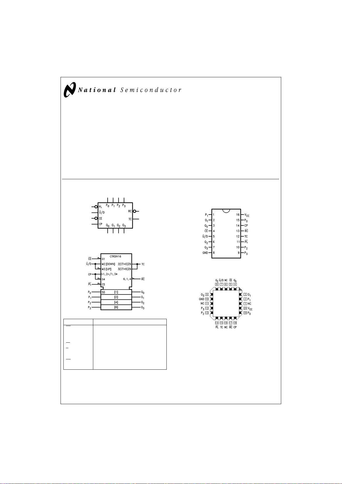
Logic Symbols
Pin Names Description
CE
Count Enable Input
CP Clock Pulse Input
P
0–P3
Parallel Data Inputs
PL
Asynchronous Parallel Load Input
U/D
Up/Down Count Control Input
Q
0–Q3
Flip-Flop Outputs
RC
Ripple Clock Output
TC Terminal Count Output
Connection Diagrams
FACT™is a trademark of Fairchild Semiconductor Corporation.
DS100279-1
IEEE/IEC
DS100279-2
Pin Assignment
for DIP and Flatpack
DS100279-3
Pin Assignment for LCC
DS100279-4
July 1998
54AC191 Up/Down Counter with Preset and Ripple Clock
© 1998 National Semiconductor Corporation DS100279 www.national.com
Page 2
Functional Description
The ’AC191 is a synchronous up/down counter. The ’AC191
is organized as a 4-bit binary counter. It contains four
edge-triggered flip-flops with internal gating and steering
logic to provide individual preset, count-up and count-down
operations.
Each circuit has an asynchronous parallel load capability
permitting the counter to be preset to any desired number.
When the Parallel Load (PL) input is LOW, information
present on the Parallel Load inputs (P0–P3) is loaded into
the counter and appears on the Q outputs. This operation
overrides the counting functions, as indicated in the Mode
Select Table.
AHIGH signal on the CE input inhibits counting. When CE is
LOW, internal state changes are initiated synchronously by
the LOW-to-HIGH transition of the clock input. The direction
of counting is determined by the U/D input signal, as indicated in the Mode Select Table. CE and U/D can be changed
with the clock in either state, provided only that the recommended setup and hold times are observed.
Two types of outputs are provided as overflow/underflow indicators. The terminal count (TC) output is normally LOW. It
goes HIGH when the circuits reach zero in the count down
mode or 15 in the count up mode. The TC output will then remain HIGH until a state change occurs, whether by counting
or presetting or until U/D is changed. The TC output should
not be used as a clock signal because it is subject to decoding spikes.
The TC signal is also used internally to enable the Ripple
Clock (RC) output. The RC output is normally HIGH. When
CE is LOW and TC is HIGH, RCoutput wil go LOW when the
clock next goes LOW and will stay LOW until the clock goes
HIGH again. This feature simplifies the design of multistage
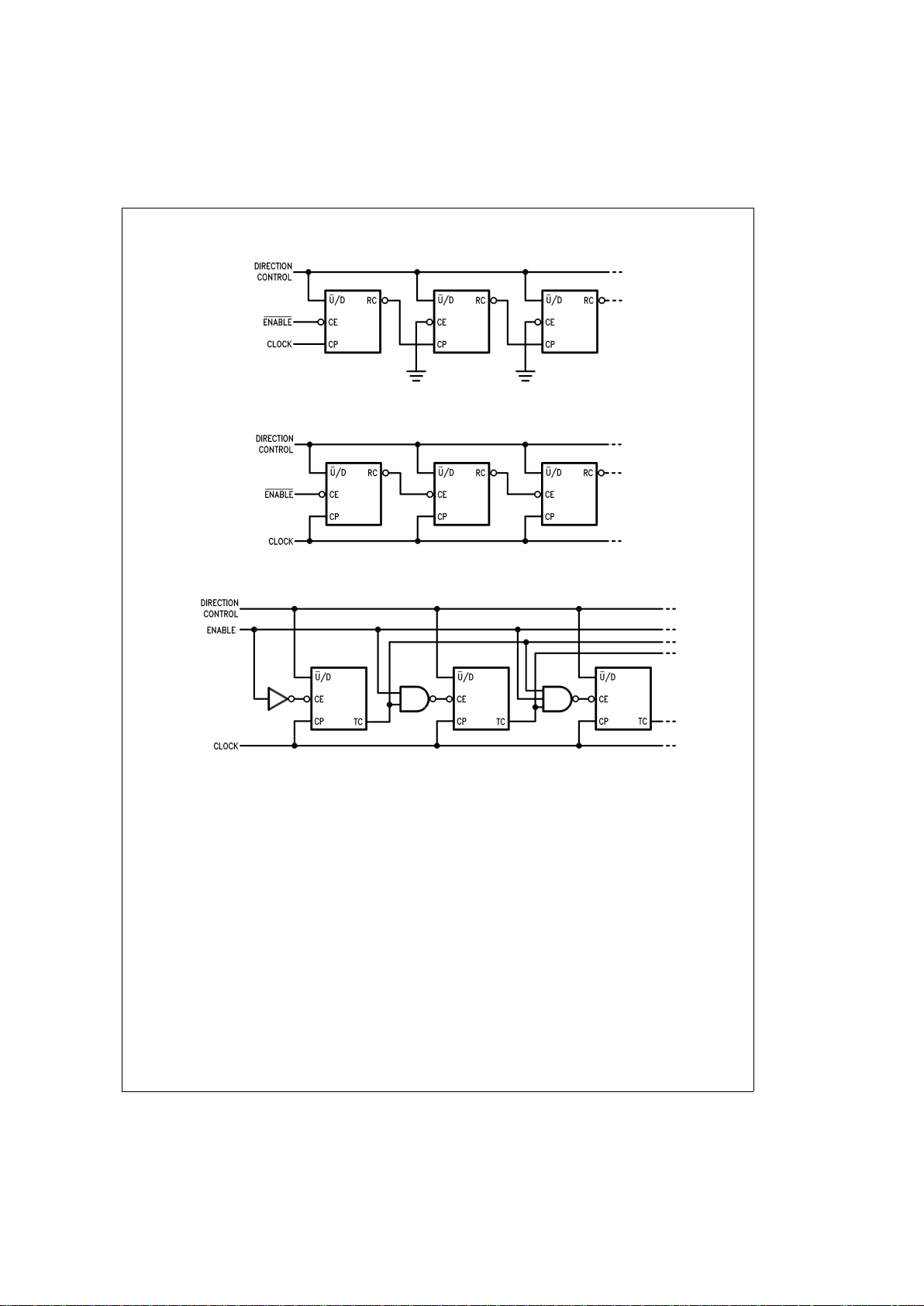
counters, as indicated in
Figure 1
and
Figure 2
.In
Figure 1
,
each RC output is used as the clock input for the next higher
stage. This configuration is particularly advantageous when
the clock source has a limited drive capability,since it drives
only the first stage. To prevent counting in all stages it is only
necessary to inhibit the first stage, since a HIGH signal on
CE inhibits the RC output pulse, as indicated in the RC Truth
Table. A disadvantage of this configuration, in some applications, is the timing skew between state changes in the first
and last stages. This represents the cumulative delay of the
clock as it ripples through the preceding stages.
A method of causing state changes to occur simultaneously
in all stages is shown in
Figure 2
. All clock inputs are driven
in parallel and the RC outputs propagate the carry/borrow
signals in ripple fashion. In this configuration the LOW state
duration of the clock must be long enough to allow the
negative-going edge of the carry/borrow signal to ripple
through to the last stage before the clock goes HIGH. There
is no such restriction on the HIGH state duration of the clock,
since the RC output of any device goes HIGH shortly after its
CP input goes HIGH.
The configuration shown in
Figure 3
avoids ripple delays and
their associated restrictions. The CE input for a given stage
is formed by combining the TC signals from all the preceding
stages. Note that in order to inhibit counting an enable signal
must be included in each carry gate. The simple inhibit
scheme of
Figure 1
and
Figure 2
doesn’t apply,because the
TC output of a given stage is not affected by its own CE.
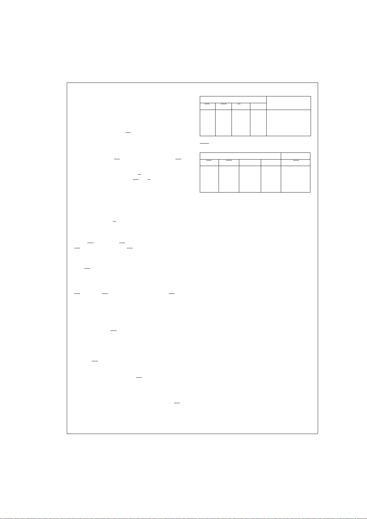
Mode Select Table
Inputs Mode
PL
CE U/D CP
HL L
N
Count Up
HL H
N
Count Down
L X X X Preset (Asyn.)
H H X X No Change (Hold)
RC Truth Table
Inputs Outputs
PL
CE TC
*
CP RC
HL H
JJ
HH X X H
HXLX H
LXXX H
*
TC is generated internally
H=HIGH Voltage Level
L=LOW Voltage Level
X=Immaterial
N
=
LOW-to-HIGH Transition
www.national.com 2
Page 3
Functional Description (Continued)
DS100279-7
FIGURE 1. N-Stage Counter Using Ripple Clock
DS100279-8
FIGURE 2. Synchronous N-Stage Counter Using Ripple Carry/Borrow
DS100279-9
FIGURE 3. Synchronous N-Stage Counter with Parallel Gated Carry/Borrow
3 www.national.com
Page 4
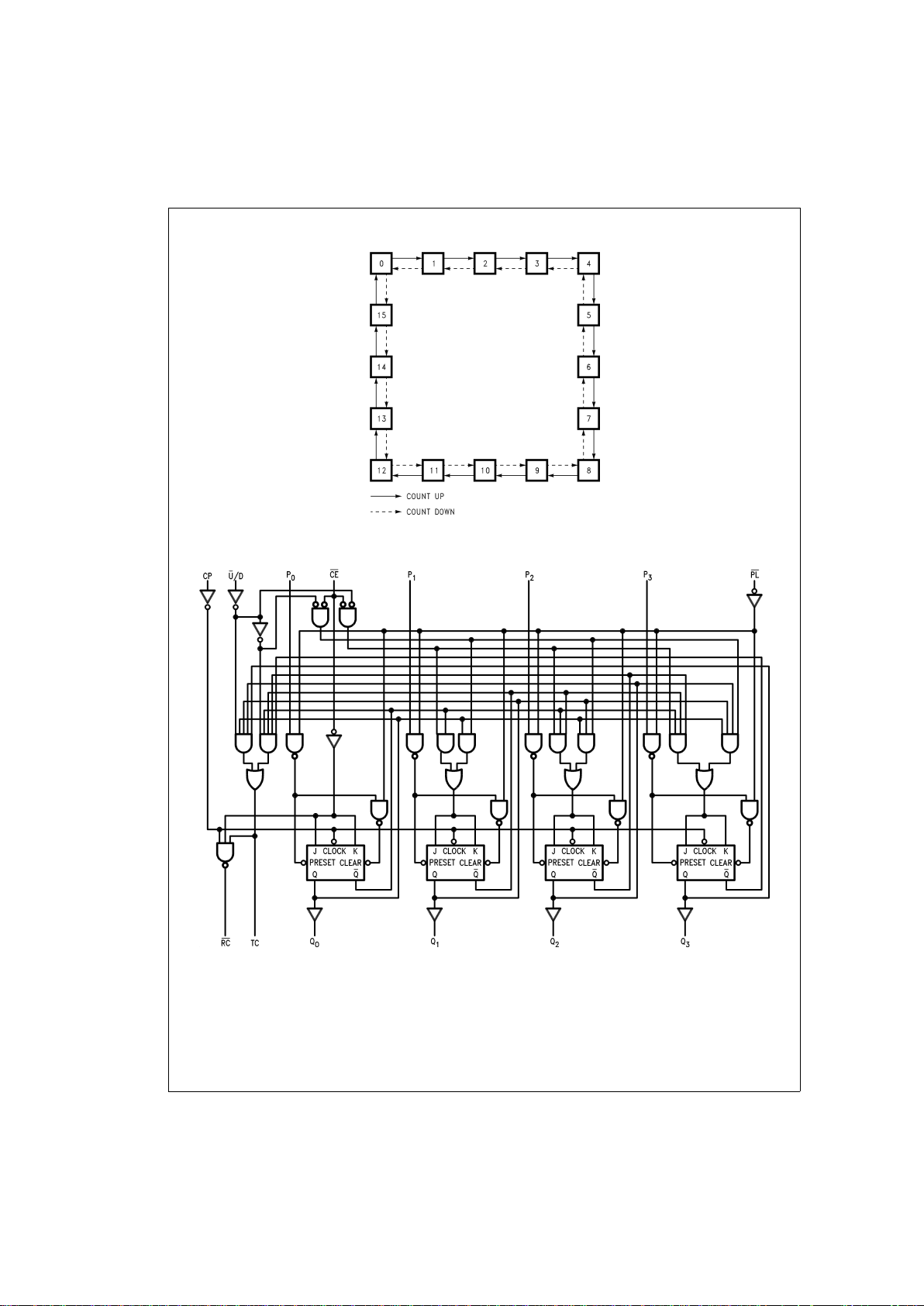
State Diagram
Logic Diagram
DS100279-5
DS100279-6
Please note that this diagram is provided only for the understanding of logic operations and should not be used to estimate propagation delays.
www.national.com 4
Page 5
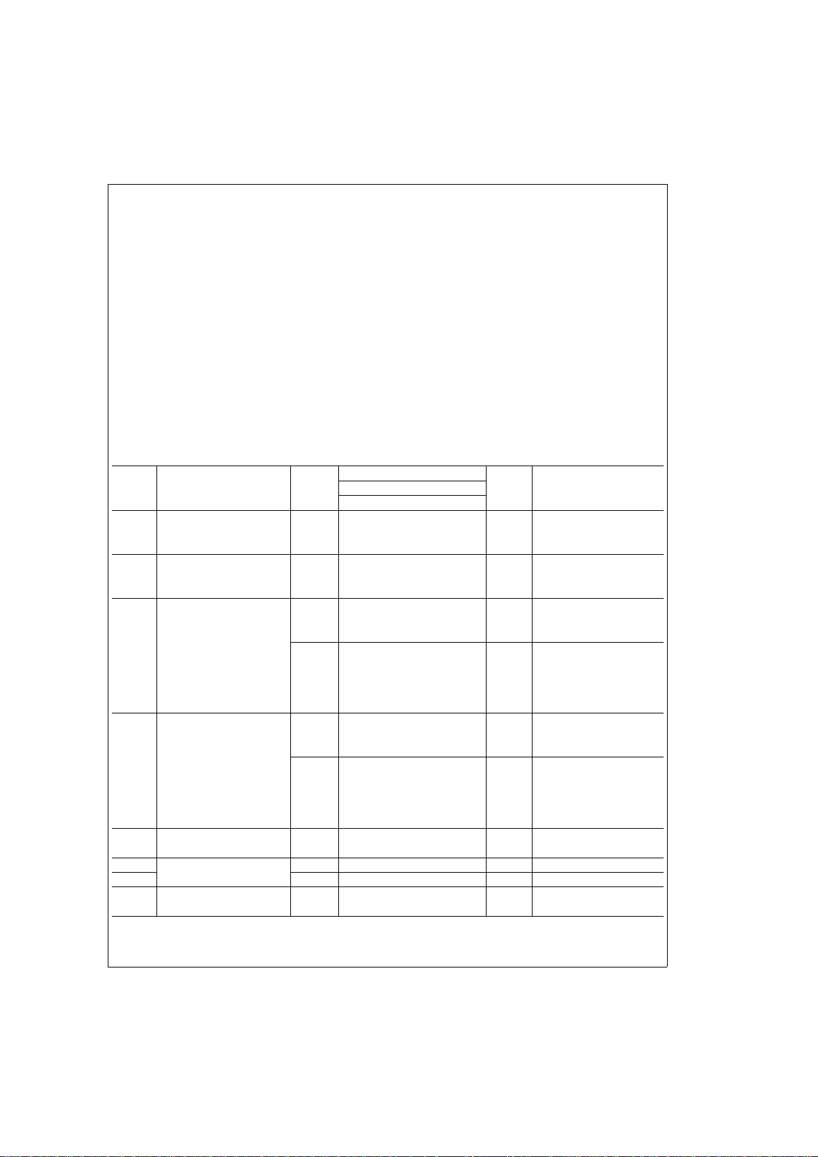
Absolute Maximum Ratings (Note 1)
If Military/Aerospace specified devices are required,
please contact the National Semiconductor Sales Office/
Distributors for availability and specifications.
Supply Voltage (V
CC
) −0.5V to +7.0V
DC Input Diode Current (I
IK
)
V
I
=
−0.5V −20 mA
V
I
=
V
CC
+ 0.5V +20 mA
DC Input Voltage (V
I
) −0.5V to VCC+ 0.5V
DC Output Diode Current (I
OK
)
V
O
=
−0.5V −20 mA
V
O
=
V
CC
+ 0.5V +20 mA
DC Output Voltage (V
O
) −0.5V to VCC+ 0.5V
DC Output Source
or Sink Current (I
O
)
±
50 mA
DC V
CC
or Ground Current
per Output Pin (I
CC
or I
GND
)
±
50 mA
Storage Temperature (T
STG
) −65˚C to +150˚C
Junction Temperature (T
J
)
CDIP 175˚C
Recommended Operating
Conditions
Supply Voltage (VCC) 2.0V to 6.0V
Input Voltage (V
I
) 0VtoV
CC
Output Voltage (VO) 0VtoV
CC
Operating Temperature (TA)
54AC −55˚C to +125˚C
Minimum Input Edge Rate (∆V/∆t)
’AC Devices
V
IN
from 30%to 70%of V
CC
V
CC
@
3.3V 4.5V, 5.5V 125 mV/ns
Note 1: Absolute maximum ratings are those values beyond which damage
to the device may occur.The databook specifications should be met, without
exception, to ensure that the system design is reliable over its power supply,
temperature, output/input loading variables. National does not recommend
operation of FACT
™
circuits outside databook specifications.
DC Characteristics for ’AC Family Devices
Symbol Parameter
V
CC
(V)
54AC
Units ConditionsT
A
=
−55˚C to +125˚C
Guaranteed Limits
V
IH
Minimum High Level Input
Voltage
3.0 2.1 V
OUT
=
0.1V
4.5 3.15 V or V
CC
− 0.1V
5.5 3.85
V
IL
Maximum Low Level Input
Voltage
3.0 0.9 V
OUT
=
0.1V
4.5 1.35 V or V
CC
− 0.1V
5.5 1.65
V
OH
Minimum High Level Output
Voltage
3.0 2.9 I
OUT
=
−50 µA
4.5 4.4 V
5.5 5.4
(Note 2) V
IN
=
V
IL
or V
IH
3.0 2.4 −12 mA
4.5 3.7 V I
OH
−24 mA
5.5 4.7 −24 mA
V
OL
Maximum Low Level Output
Voltage
3.0 0.1 I
OUT
=
50 µA
4.5 0.1 V
5.5 0.1
(Note 2) V
IN
=
V
IL
or V
IH
3.0 0.50 12 mA
4.5 0.50 V I
OL
24 mA
5.5 0.50 24 mA
I
IN
Maximum Input 5.5
±
1.0 µA V
I
=
V
CC
, GND
Leakage Current
I
OLD
(Note 3) Minimum Dynamic 5.5 50 mA V
OLD
=
1.65V Max
I
OHD
Output Current 5.5 −50 mA V
OHD
=
3.85V Min
I
CC
Maximum Quiescent 5.5 80.0 µA V
IN
=
V
CC
Supply Current or GND
5 www.national.com
Page 6
DC Characteristics for ’AC Family Devices (Continued)
Note 2: All outputs loaded; thresholds on input associated with output under test.
Note 3: Maximum test duration 2.0 ms, one output loaded at a time.
Note 4: I
IN
and I
CC
@
3.0V are guaranteed to be less than or equal to the respective [email protected] VCC.
I
CC
for 54AC@25˚C is identical to 74AC@25˚C.
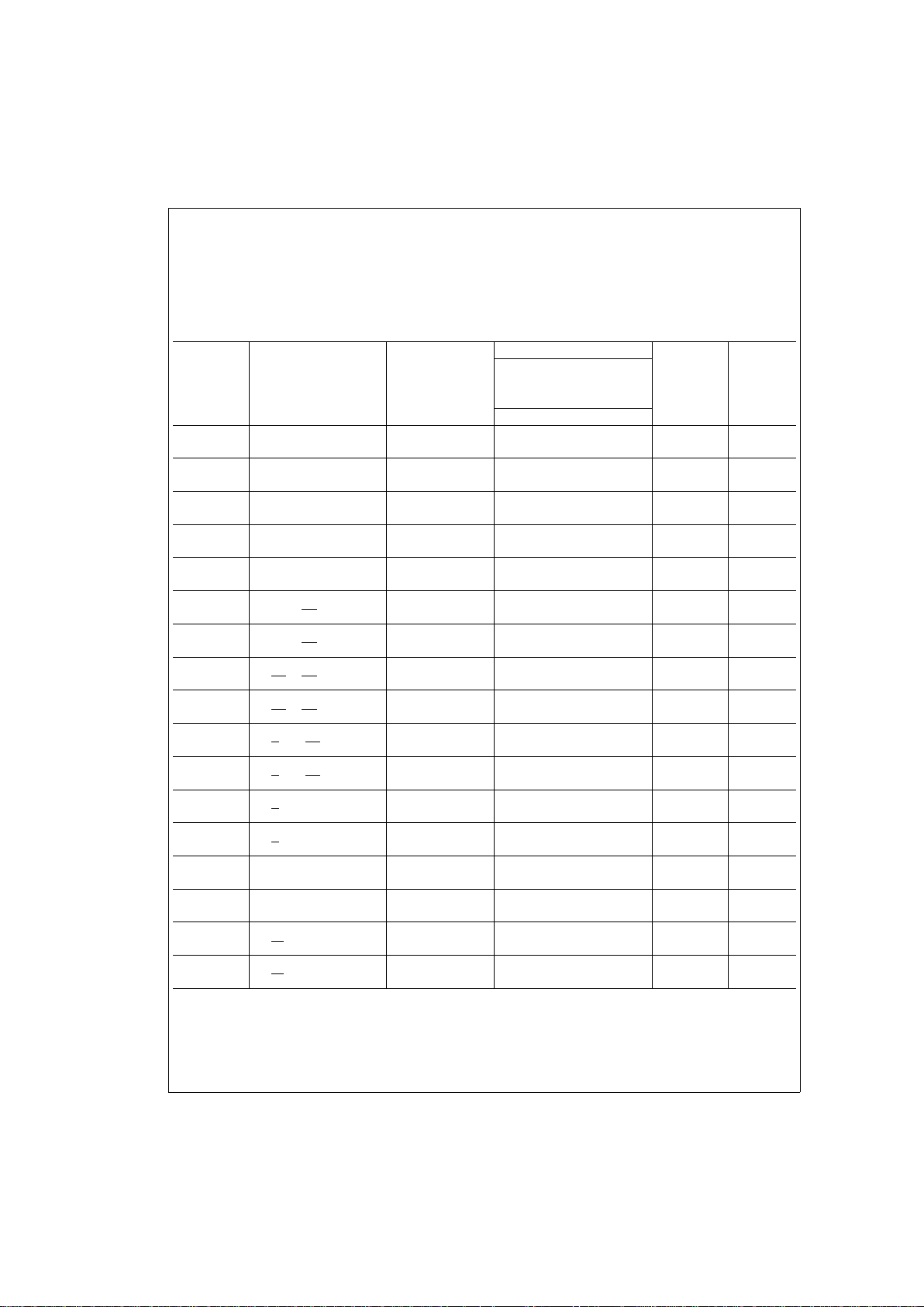
AC Electrical Characteristics
54AC
V
CC
T
A
=
−55˚C
to +125˚C
C
L
=
50 pF
Fig.
No.
Symbol Parameter (V) Units
(Note 5)
Min Max
f
max
Maximum Count 3.3 55 MHz
Frequency 5.0 80
t
PLH
Propagation Delay 3.3 1.0 16.5 ns
CP to Q
n
5.0 1.0 12.0
t
PHL
Propagation Delay 3.3 1.0 16.0 ns
CP to Q
n
5.0 1.0 12.0
t
PLH
Propagation Delay 3.3 1.0 19.5 ns
CP to TC 5.0 1.0 14.0
t
PHL
Propagation Delay 3.3 1.0 19.0 ns
CP to TC 5.0 1.0 14.5
t
PLH
Propagation Delay 3.3 1.0 14.0 ns
CP to RC
5.0 1.0 10.5
t
PHL
Propagation Delay 3.3 1.0 12.5 ns
CP to RC
5.0 1.0 9.5
t
PLH
Propagation Delay 3.3 1.0 14.0 ns
CE to RC
5.0 1.0 10.0
t
PHL
Propagation Delay 3.3 1.0 12.5 ns
CE to RC
5.0 1.0 9.5
t
PLH
Propagation Delay 3.3 1.0 14.5 ns
U/D to RC
5.0 1.0 11.0
t
PHL
Propagation Delay 3.3 1.0 15.0 ns
U/D to RC
5.0 1.0 11.0
t
PLH
Propagation Delay 3.3 1.0 14.0 ns
U/D to TC
5.0 1.0 10.5
t
PHL
Propagation Delay 3.3 1.0 13.5 ns
U/D to TC
5.0 1.0 10.0
t
PLH
Propagation Delay 3.3 1.0 16.5 ns
P
n
to Q
n
5.0 1.0 11.5
t
PHL
Propagation Delay 3.3 1.0 15.5 ns
P
n
to Q
n
5.0 1.0 10.5
t
PLH
Propagation Delay 3.3 1.0 18.0 ns
PL to Q
n
5.0 1.0 12.5
t
PHL
Propagation Delay 3.3 1.0 15.5 ns
PL to Q
n
5.0 1.0 11.5
Note 5: Voltage Range 3.3 is 3.3V±0.3V
Voltage Range 5.0 is 5.0V
±
0.5V
www.national.com 6
Page 7
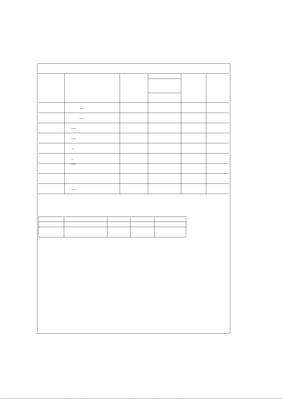
AC Operating Requirements
Symbol Parameter
V
CC
(V)
(Note 6)
54AC
Units
Fig.
No.
T
A
=
−55˚C
to +125˚C
C
L
=
50 pF
Guaranteed
Minimum
t
s
Setup Time, HIGH or LOW 3.3 4.0 ns
P
n
to PL 5.0 3.0
t
h
Hold Time, HIGH or LOW 3.3 1.5 ns
P
n
to PL 5.0 2.0
t
s
Setup Time, LOW 3.3 9.0 ns
CE to CP
5.0 6.0
t
h
Hold Time, LOW 3.3 0 ns
CE to CP
5.0 0.5
t
s
Setup Time, HIGH or LOW 3.3 10.5 ns
U/D to CP
5.0 7.5
t
h
Hold Time, HIGH or LOW 3.3 0 ns
U/D to CP
5.0 1.0
t
w
PL Pulse Width, LOW 3.3 5.0 ns
5.0 5.0
t
w
CP Pulse Width, LOW 3.3 6.0 ns
5.0 6.0
t
rec
Recovery Time 3.3 1.5 ns
PL to CP
5.0 1.0
Note 6: Voltage Range 3.3 is 3.3V±0.3V
Voltage Range 5.0 is 5.0V
±
0.5V
Capacitance
Symbol Parameter Typ Units Conditions
C
IN
Input Capacitance 4.5 pF V
CC
=
OPEN
C
PD
Power Dissipation 75.0 pF V
CC
=
5.0V
Capacitance
7 www.national.com
Page 8

8
Page 9
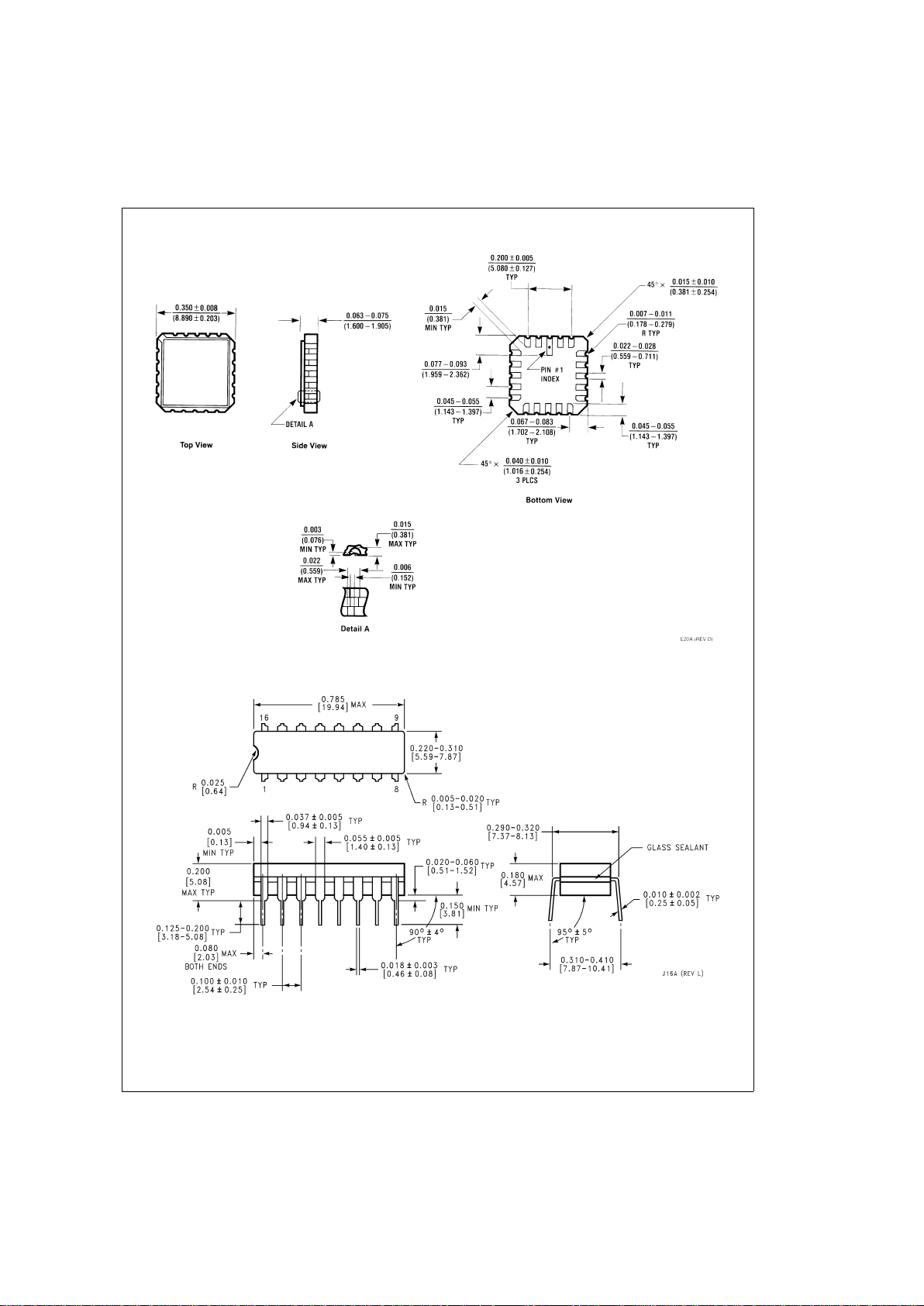
Physical Dimensions inches (millimeters) unless otherwise noted
20 Terminal Ceramic Leadless Chip Carrier (L)
NS Package Number E20A
16 Lead Ceramic Dual-In-Line Package (D)
NS Package Number J16A
9 www.national.com
Page 10
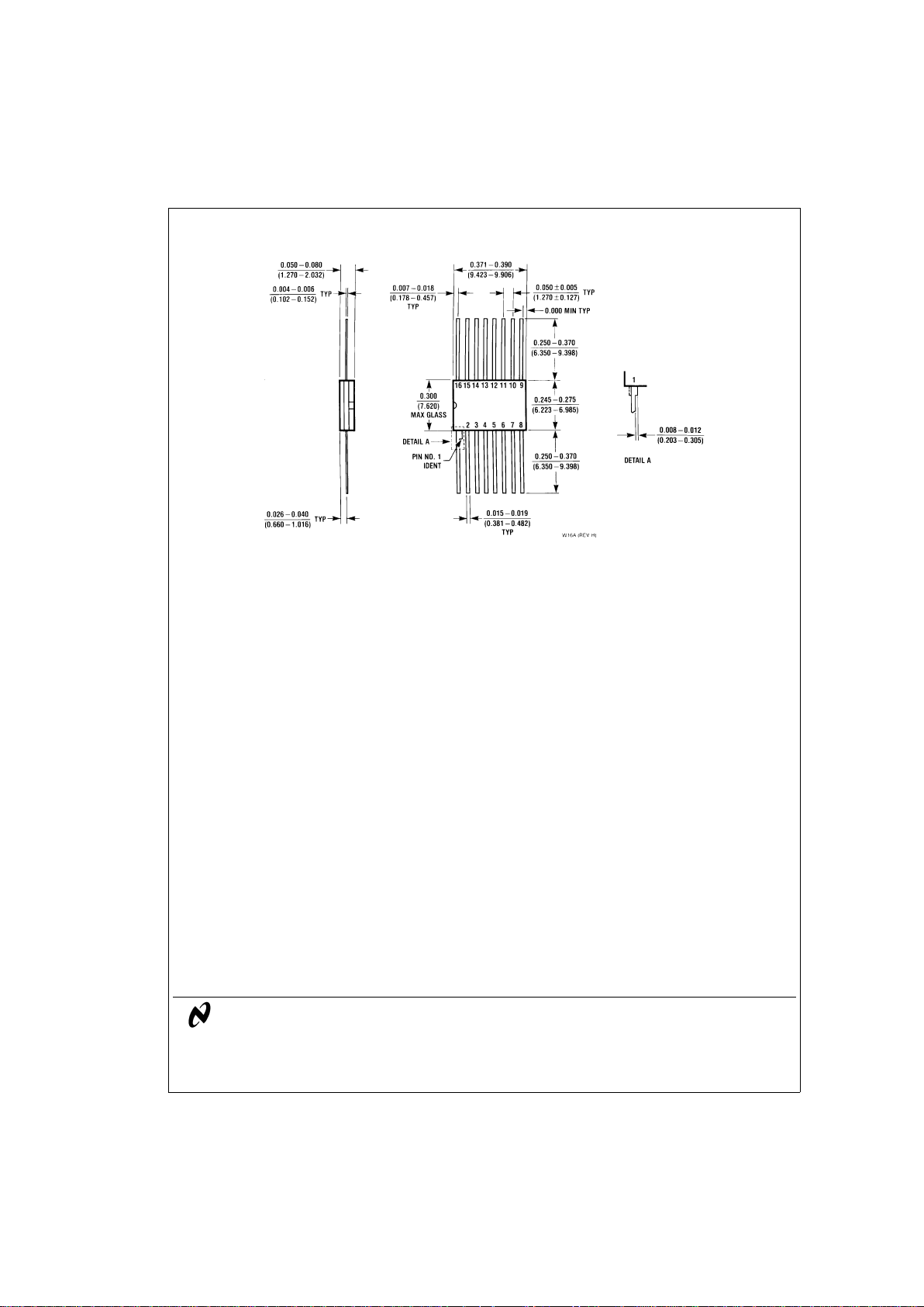
Physical Dimensions inches (millimeters) unless otherwise noted (Continued)
LIFE SUPPORT POLICY
NATIONAL’S PRODUCTS ARE NOT AUTHORIZED FOR USE AS CRITICAL COMPONENTS IN LIFE SUPPORT DEVICES OR SYSTEMS WITHOUT THE EXPRESS WRITTEN APPROVAL OF THE PRESIDENT OF NATIONAL SEMICONDUCTOR CORPORATION. As used herein:
1. Life support devices or systems are devices or systems which, (a) are intended for surgical implant into
the body, or (b) support or sustain life, and whose failure to perform when properly used in accordance
with instructions for use provided in the labeling, can
be reasonably expected to result in a significant injury
to the user.
2. A critical component in any component of a life support
device or system whose failure to perform can be reasonably expected to cause the failure of the life support
device or system, or to affect its safety or effectiveness.
National Semiconductor
Corporation
Americas
Tel: 1-800-272-9959
Fax: 1-800-737-7018
Email: [email protected]
www.national.com
National Semiconductor
Europe
Fax: +49 (0) 1 80-530 85 86
Email: [email protected]
Deutsch Tel: +49 (0) 1 80-530 85 85
English Tel: +49 (0) 1 80-532 78 32
Français Tel: +49 (0) 1 80-532 93 58
Italiano Tel: +49 (0) 1 80-534 16 80
National Semiconductor
Asia Pacific Customer
Response Group
Tel: 65-2544466
Fax: 65-2504466
Email: [email protected]
National Semiconductor
Japan Ltd.
Tel: 81-3-5620-6175
Fax: 81-3-5620-6179
16 Lead Ceramic Flatpak (F)
NS Package Number W16A
54AC191 Up/Down Counter with Preset and Ripple Clock
National does not assume any responsibility for use of any circuitry described, no circuit patent licenses are implied and National reserves the right at any time without notice to change said circuitry and specifications.
 Loading...