

Page 1
DS9627
Dual Line Receiver
General Description
The DS9627 is a dual-line receiver which meets the electrical interface specifications of EIA RS-232C and
MIL-STD-188C. The input circuitry accommodates
±
25V input signals and the differential inputs allow user selectionof
either inverting or non-inverting logic for the receiver operation. The DS9627 provides both a selectable hysteresis
range and selectable receiver input resistance. When pin 1
is tied to V
−
, the typical switching points are at 2.6V and
−2.6V, thus meeting RS-232-C requirements. When pin 1 is
open, the typical switching points are at 50 µA and −50 µA,
thus satisfying the requirements of MIL-STD-188C LOW
level interface. Connecting the RA and/or RB pins to the (−)
input yields an input impedance in the range of 3 kΩ to 7 kΩ
and satisfies RS-232-C requirements; leaving RA and/or RB
pins unconnected, the input resistance will be greater than
6kΩto satisfy MIL-STD-188C.
The output circuitry is TTL/DTL compatible and will allow
“collector-dotting” to generate the wired-OR function. A TTL/
DTL strobe is also provided for each receiver.
Features
n EIA RS-232-C input standards
n MIL-STD-188C input standards
n Variable hysteresis control
n High common mode rejection
n R control (5 kΩ or 10 kΩ)
n Wired-OR capability
n Choice of inverting and non-inverting inputs
n Outputs and strobe TTL compatible
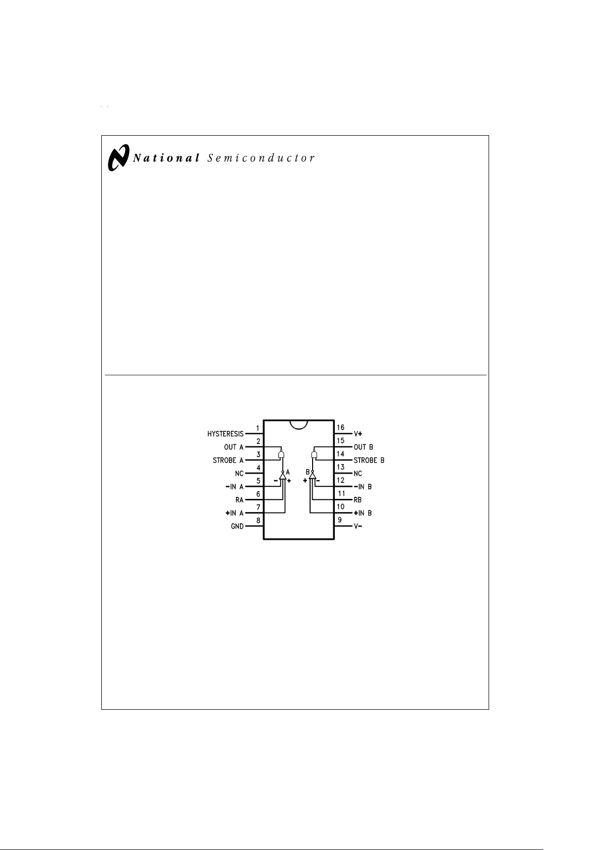
Connection Diagram
16-Lead DIP
DS009761-1
Top View
Order Number DS9627MJ/883
See NS Package Number J16A
For Complete Military 883 Specifications, see RETS Data Sheet.
February 1996
DS9627 Dual Line Receiver
© 1999 National Semiconductor Corporation DS009761 www.national.com
Page 2
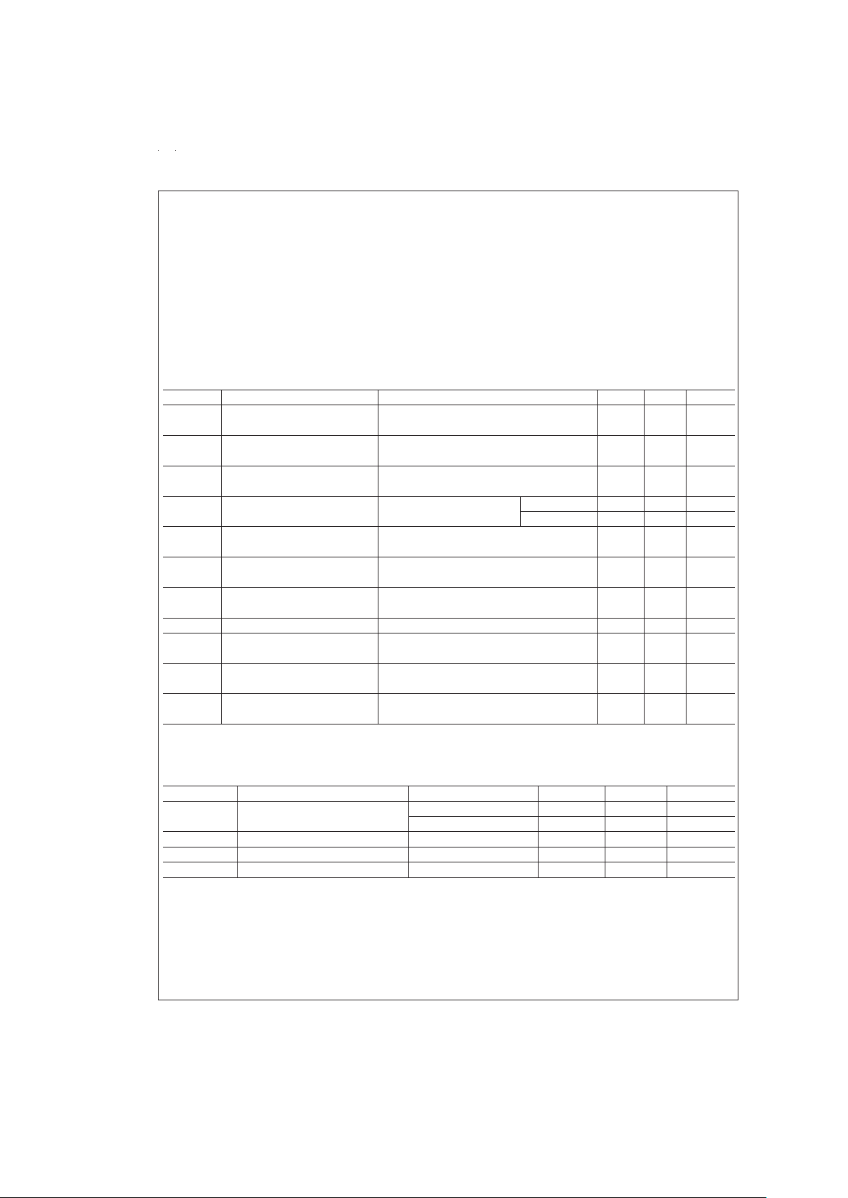
Absolute Maximum Ratings (Note 1)
If Military/Aerospace specified devices are required,
please contact the National Semiconductor Sales Office/
Distributors for availability and specifications.
Storage Temperature Range −65˚C to +175˚C
Operating Temperature Range −55˚C to +125˚C
Lead Temperature (Soldering, 60 sec.) 300˚C
Internal Power Dissipation (Note 5) 400 mW
V
+
to GND 0V to +15V
V
−
to GND 0V to −15V
Input Voltage Referred to GND
±
25V
Strobe to GND −0.5V to +5.5V
Applied Output Voltage −0.5V to +15V
Operating Conditions
Min Max Units
Supply Voltage (V
CC
) 4.5 5.5 V
Temperature (T
A
) −55 +125 ˚C
Electrical Characteristics (Notes 2, 3)
Hysteresis, −IN A, −IN B, RA and RB Open for MIL-STD-188C, unless otherwise specified
Symbol Characteristics Conditions Min Max Units
V
OL
Output Voltage LOW V
+
=
10.8V, V
−
=
−13.2V, 0.4 V
V
I
+
=
0.6V, I
OL
=
6.4 mA
V
OH
Output Voltage HIGH V
+
=
10.8V, V
−
=
−13.2V, 2.4 V
V
I
+
=
0.6V, I
OH
=
−0.5 mA
I
OS
Output Short Circuit V+=13.2V, V
−
=
−10.8V, −3.0 mA
Current (Note 4) V
I+
=
0.6V, V
O
=
0V
I
IH
(ST) Input Current HIGH V
+
=
10.8V, V
ST
=
2.4V 40 µA
(Strobe) V
−
=
−13.2V, V
I
+
=
0.6V V
ST
=
5.5V 1.0 mA
R
I
Input Resistance V
+
=
13.2V, V
−
=
−13.2V, 6.0 kΩ
−3.0V ≤ V
I
+
≤ 3.0V
I
TH+
Positive Threshold Current
±
10.8V ≤ VCC≤±13.2V, 100 µA
V
O
=
2.4V
I
TH
−
Negative Threshold Current
±
10.8V ≤ VCC≤±13.2V, −100 µA
V
O
=
0.4V
V
IL
(ST) Input Voltage LOW (Strobe) V
I
+
=
−0.6V 0.8 V
V
IH
(ST) Input Voltage HIGH (Strobe) V
+
=
13.2V, V
−
=
−10.8V, 2.0 V
V
I
+
=
−0.6V
I
+
Positive Supply Current
±
10.8V ≤ VCC≤±13.2V 18 mA
V
I
+
=
−0.6V
I
−
Negative Supply Current
±
10.8V ≤ VCC≤±13.2V −16 mA
V
I
+
=
0.6V
Electrical Characteristics
+IN A and −IN B connected to ground, RA and RB connected to −IN A and −IN B and Hysteresis connected to V−for
RS-232C, unless otherwise specified
Symbol Characteristics Conditions Min Max Units
R
I
Input Resistance 3.0V ≤ VI≤ 25V 3.0 7.0 kΩ
−3.0V ≤ V
I
≤ −25V 3.0 7.0 kΩ
V
I
Input Voltage −2.0 2.0 V
V
TH+
Positive Threshold Voltage 3.0 V
V
TH−
Negative Threshold Voltage −3.0 V
Note 1: “AbsoluteMaximum Ratings” are those values beyond which the safety of the device cannot be guaranteed. They are not meant to imply that the devices
should be operated at these limits. The tables of “Electrical Characteristics” provide conditions for actual device operation.
Note 2: Unless otherwise specified Min/Max limits apply across the −55˚C to +125˚C temperature range.
Note 3: All currents into device pins are positive; all currents out of device pins are negative. All voltages are referenced to ground unless otherwise specified.
Note 4: Only one output at a time should be shorted.
Note 5: Rating applies to ambient temperatures up to +125˚C. Above 125˚C ambient, derate linearity at 120˚C/W.
www.national.com 2
Page 3

Electrical Characteristics
V
CC
=
±
12V for MIL-STD-188C and RS-232C, T
A
=
25˚C
Symbol Characteristics Conditions Min Max Units
t
PLH
Propagation Delay to High Level See
Figure 1
250 ns
t
PHL
Propagation Delay to Low Level See
Figure 1
250 ns
DS009761-2
15 pF includes jig capacitance. All diodes are FD777 or equivalent.
DS009761-3
PRR=10 kHz
PW=50 µs
t
r
=
t
f
=
5ns
FIGURE 1. Switching Time Test Circuit and Waveforms
www.national.com3
Page 4
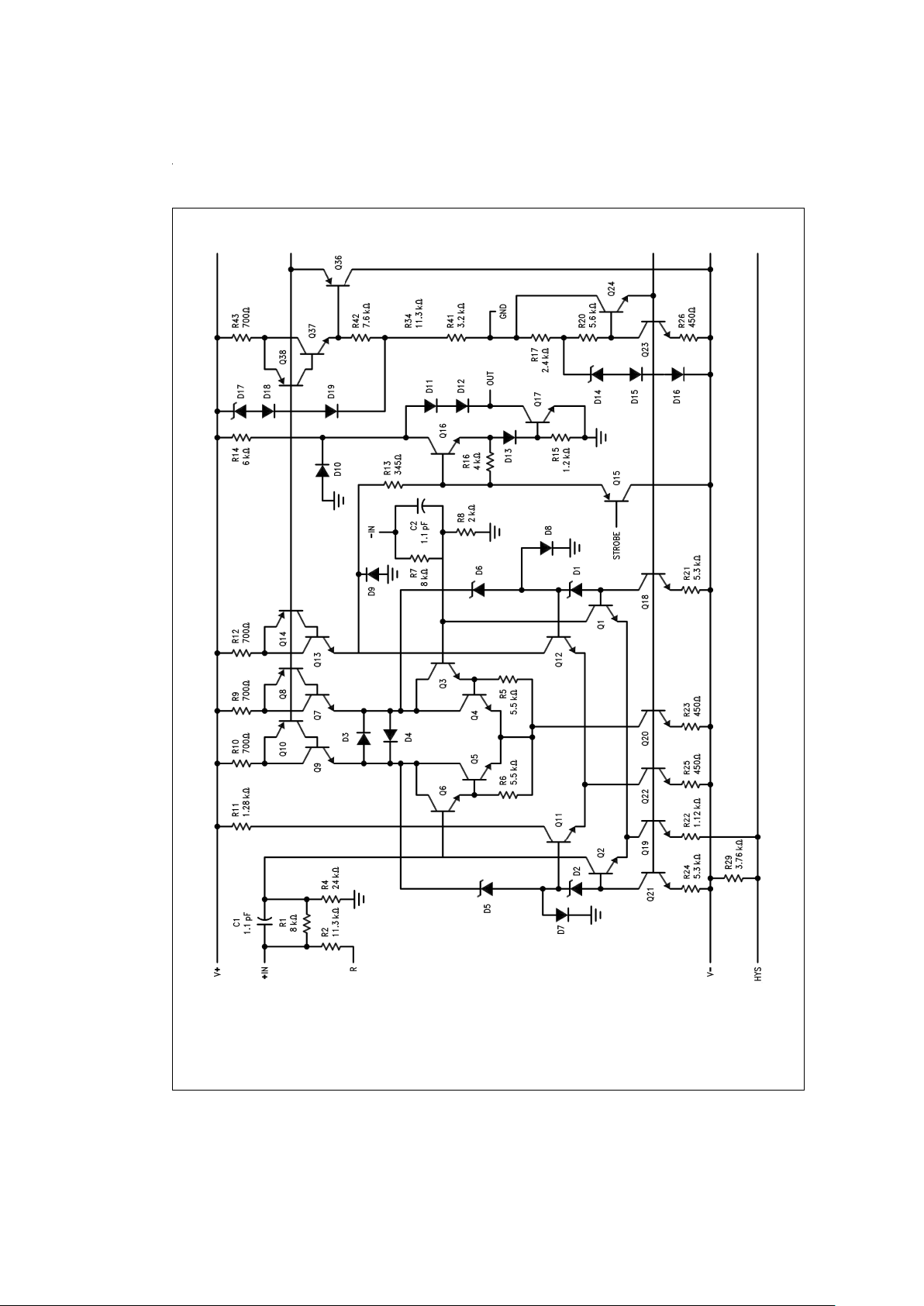
Equivalent Circuit (
1
⁄2of Circuit)
DS009761-4
www.national.com 4
Page 5
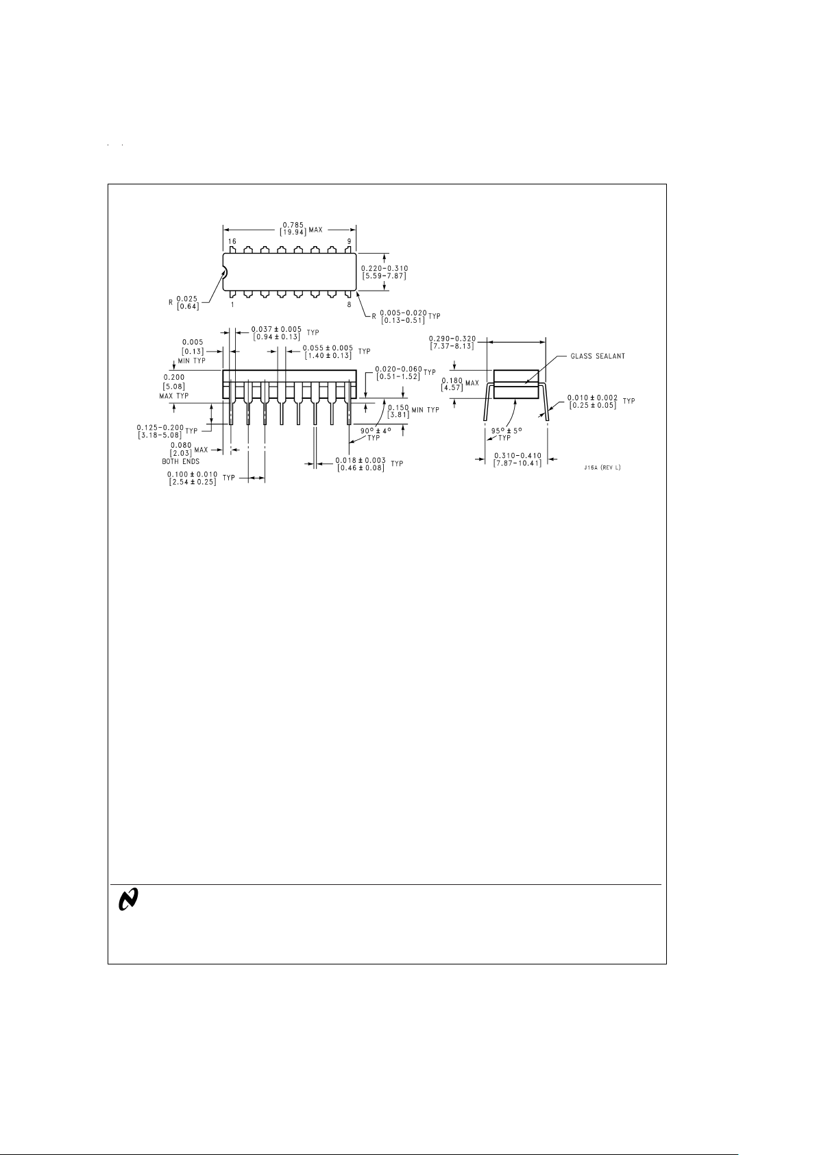
Physical Dimensions inches (millimeters) unless otherwise noted
LIFE SUPPORT POLICY
NATIONAL’S PRODUCTS ARE NOT AUTHORIZED FOR USE AS CRITICAL COMPONENTS IN LIFE SUPPORT
DEVICES OR SYSTEMS WITHOUT THE EXPRESS WRITTEN APPROVAL OF THE PRESIDENT AND GENERAL
COUNSEL OF NATIONAL SEMICONDUCTOR CORPORATION. As used herein:
1. Life support devices or systems are devices or
systems which, (a) are intended for surgical implant
into the body, or (b) support or sustain life, and
whose failure to perform when properly used in
accordance with instructions for use provided in the
labeling, can be reasonably expected to result in a
significant injury to the user.
2. A critical component is any component of a life
support device or system whose failure to perform
can be reasonably expected to cause the failure of
the life support device or system, or to affect its
safety or effectiveness.
National Semiconductor
Corporation
Americas
Tel: 1-800-272-9959
Fax: 1-800-737-7018
Email: [email protected]
National Semiconductor
Europe
Fax: +49 (0) 1 80-530 85 86
Email: [email protected]
Deutsch Tel: +49 (0) 1 80-530 85 85
English Tel: +49 (0) 1 80-532 78 32
Français Tel: +49 (0) 1 80-532 93 58
Italiano Tel: +49 (0) 1 80-534 16 80
National Semiconductor
Asia Pacific Customer
Response Group
Tel: 65-2544466
Fax: 65-2504466
Email: [email protected]
National Semiconductor
Japan Ltd.
Tel: 81-3-5639-7560
Fax: 81-3-5639-7507
www.national.com
Ceramic Dual-In-Line Package
Order Number DS9627MJ/883
NS Package Number J16A
DS9627 Dual Line Receiver
National does not assume any responsibility for use of any circuitry described, no circuit patent licenses are implied and National reserves the right at any time without notice to change said circuitry and specifications.
 Loading...