

Page 1
VHF / UHF wide band amplifier
Features
• Super compact package;
(1.4 × 0.8 × 0.59mm)
• Capable low voltage operation ;
(VCE = 1V)
Outline
2SC5544
Silicon NPN Epitaxial
ADE-208-691 (Z)
1st. Edition
Nov. 1998
Note: Marking is “YZ-”.
MFPAK
3
1
2
1. Emitter
2. Base
3. Collector
Page 2
2SC5544
C
C
C
Absolute Maximum Ratings (Ta = 25°C)
Item Symbol Ratings Unit
Collector to base voltage V
Collector to emitter voltage V
Emitter to base voltage V
Collector current I
CBO
CEO
EBO
C
Collector power dissipation Pc 80 mW
Junction temperature Tj 150 °C
Storage temperature Tstg –55 to +150 °C
Electrical Characteristics (Ta = 25°C)
Item Symbol Min Typ Max Unit Test Conditions
Collector to base breakdown
V
(BR)CBO
voltage
Collector cutoff current I
Collector cutoff current I
Emitter cutoff current I
DC current transfer ratio h
CBO
CEO
EBO
FE
Collector output capacitance Cob — 0.88 1.4 pF V
Gain bandwidth product f
T
Power gain PG 8 11.6 — dB V
Noise figure NF — 1.0 2.0 dB V
15——V I
——1 µAV
——1 mAV
——10µAV
85 — 170 V VCE = 1V , IC = 5mA
3 6 — GHz VCE = 1V , IC = 5mA
15 V
8V
1.5 V
50 mA
= 10µA , IE = 0
C
= 12V , IE = 0
CB
= 8V , RBE = ∞
CE
= 1.5V , IC = 0
EB
= 1V , IE = 0
B
f = 1MHz
= 1V, IC = 5mA
E
f = 900MHz
= 1V, IC = 5mA
E
f = 900MHz
2
Page 3
2SC5544
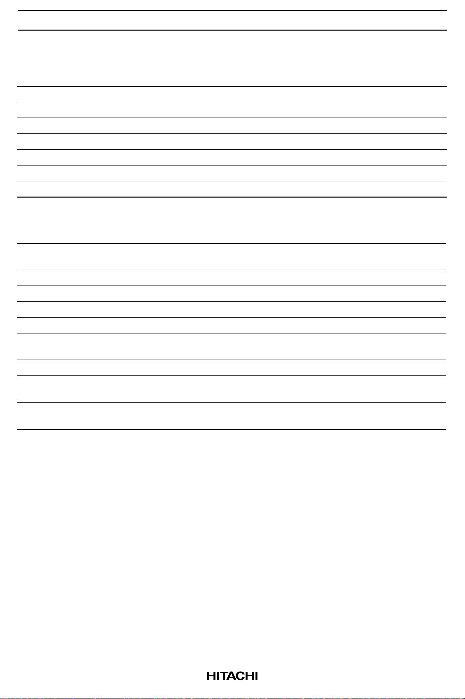
Maximum Collector Dissipation Curve
160
120
80
40
Collector Power Dissipation Pc (mW)
0
50 100 150 200
Ambient Temperature Ta (°C)
Collector Output Capacitance vs.
2.0
1.6
Collector to Base Voltage
I = 0
f = 1MHz
DC Current Transfer Ratio vs.
200
FE
Collector Current
V = 1 V
CE
100
DC Current Transfer Ratio h
0
50
25
1
10
Collector Current I (mA)
20
C
100
Gain Bandwidth Product vs.
20
E
Collector Current
V = 1 V
CE
16
T
1.2
0.8
0.4
0
Collector Output Capacitance Cob (pF)
0.2 0.5 2
0.1 1 10
Collector to Base Voltage V (V)
CB
12
8
4
Gain Bandwidth Product f (GHz)
0
5
12 5
Collector Current I (mA)
10 20
50 100
C
3
Page 4
2SC5544
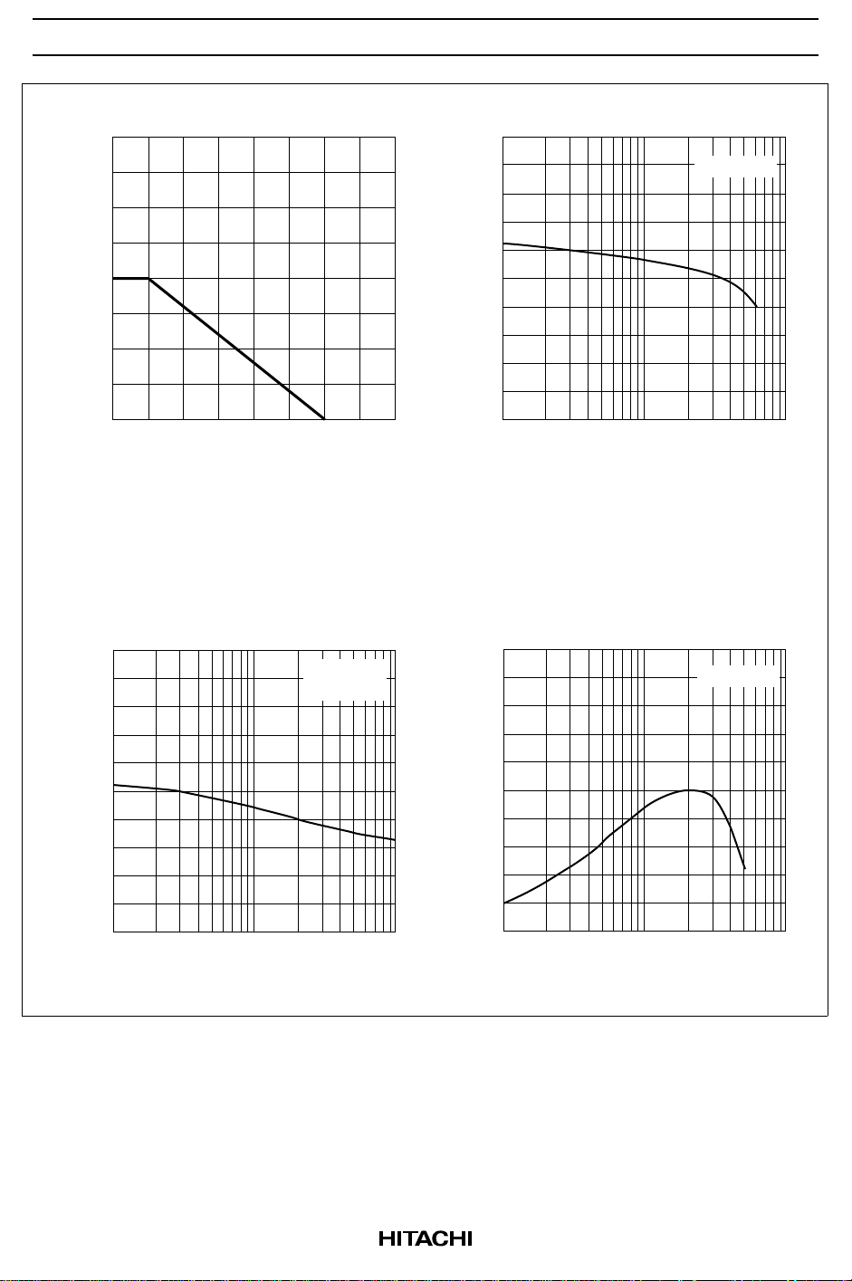
Power Gain vs. Collector Current
20
16
12
8
4
Power Gain PG (dB)
0
2
1
5
Collector Current I (mA)
S Parameter vs. Collector Current
21
20
V = 1 V
CE
f = 900MHz
20
10 50 100
C
Noise Figure vs. Collector Current
5
4
3
2
Noise Figure NF (dB)
1
0
25
1
Collector Current I (mA)
10
V = 1 V
CE
f = 900MHz
20
50
C
100
16
2
21
12
8
4
21
S parameter |S | (dB)
0
25 20
1 10 100
Collector Current I (mA)
V = 1 V
CE
f = 1GHz
50
C
4
Page 5
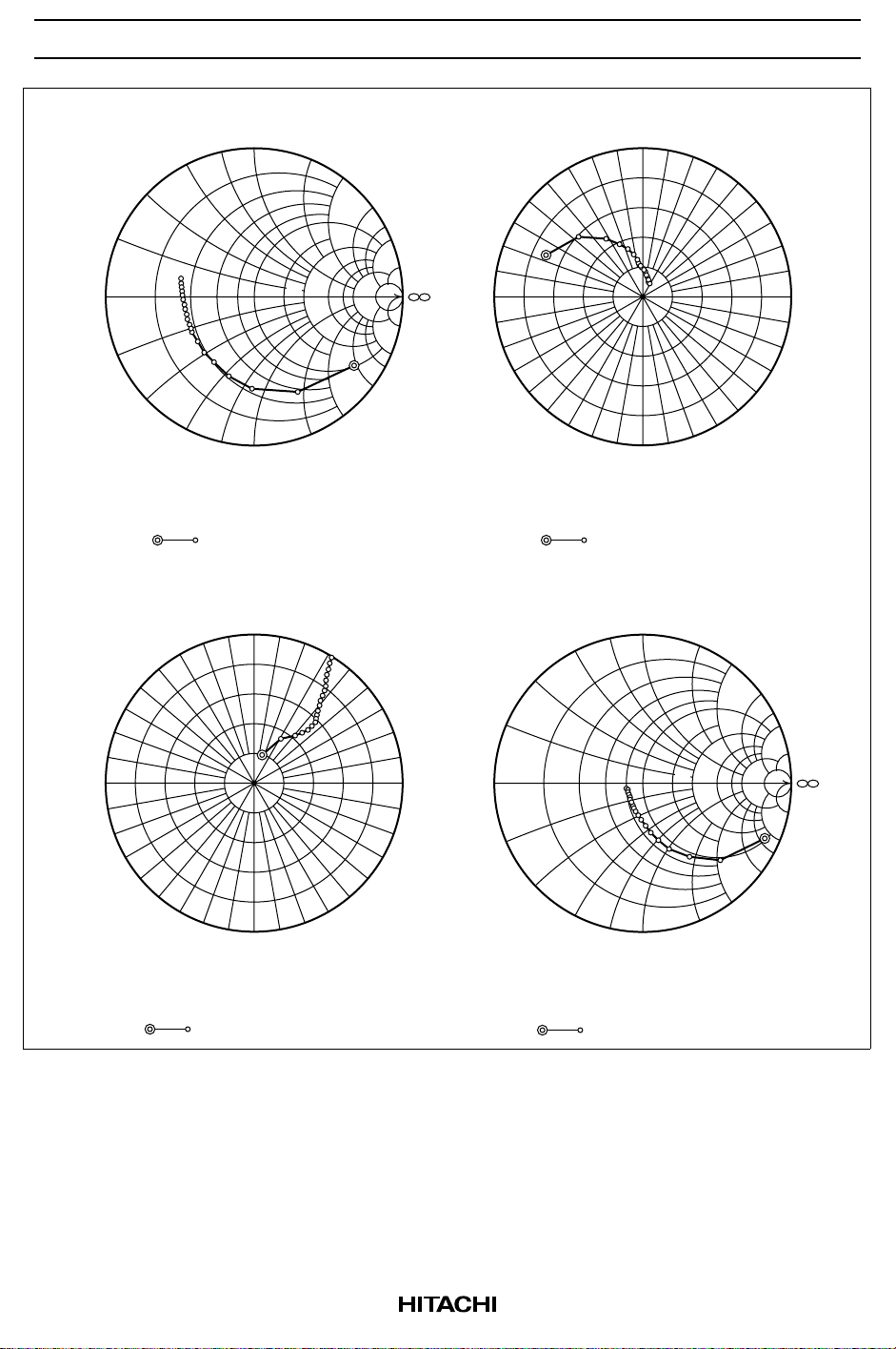
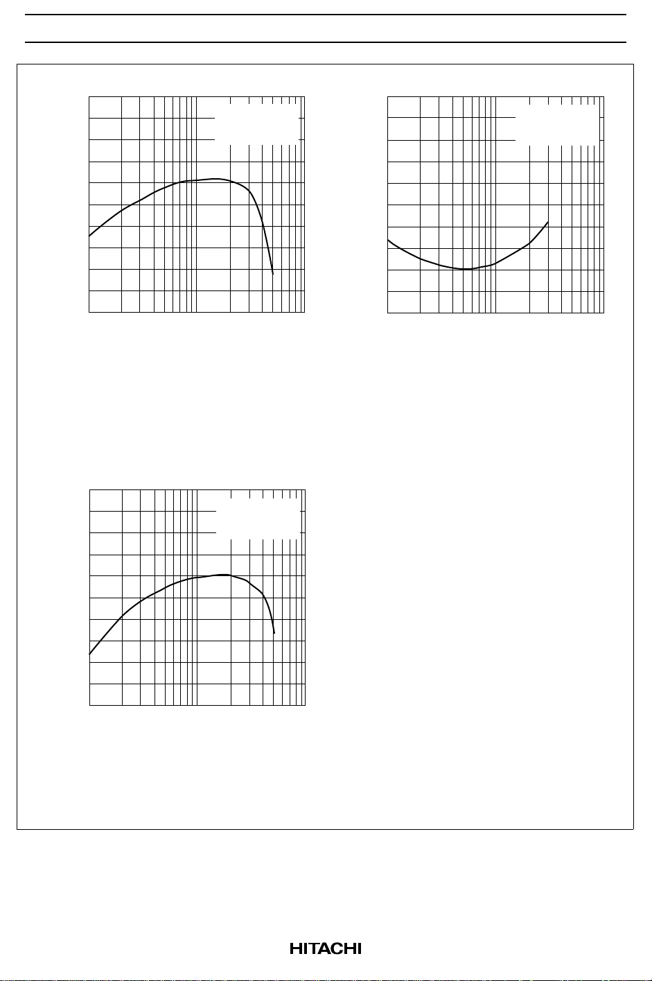
2SC5544
180°
S11 Parameter vs. Frequency
.8
.6
.4
.2
0
–.2
.2
–.4
Condition :
.6
.4
.8
–.6
–.8
–1
V = 1 V , I = 5mA
CE
100 to 2000 MHz (100 MHz step)
S12 Parameter vs. Frequency S22 Parameter vs. Frequency
120°
150°
–150°
–120°
Condition :
100 to 2000 MHz (100 MHz step)
–90°
V = 1 V , I = 5mA
CE
1
90°
1.5
1
1.5
2
3
4
234
–1.5
C
10
5
–4
–3
–2
Scale: 0.04 / div.
60°
30°
–30°
–60°
C
5
–5
10
–10
0°
180°
S21 Parameter vs. Frequency
90°
120°
150°
–150°
–120°
Condition :
100 to 2000 MHz (100 MHz step)
.6
.4
.2
0
–.2
.2
–.4
–.6
Condition :
100 to 2000 MHz (100 MHz step)
–90°
V = 1 V , I = 5mA
CE
1
.8
.6
.4
.8
–.8
–1
V = 1 V , I = 5mA
CE
1.5
1
Scale: 4 / div.
60°
–60°
C
1.5
2
234
5
–2
–1.5
C
3
10
–3
30°
–30°
4
–4
0°
5
10
–10
–5
5
Page 6
2SC5544
Sparameter (VCE = 1V, IC = 5mA, Zo = 50Ω)
S11 S21 S12 S22
f (MHz) MAG ANG MAG ANG MAG ANG MAG ANG
100 0.806 –34.7 14.09 156.3 0.0395 71.3 0.905 –24.2
200 0.706 –66.0 11.64 136.7 0.0691 57.5 0.739 –44.3
300 0.617 –90.3 9.35 122.8 0.0860 49.4 0.586 –58.1
400 0.562 –108.0 7.66 113.8 0.0965 45.8 0.474 –67.6
500 0.527 –121.9 6.40 106.7 0.104 44.3 0.392 –74.9
600 0.500 –133.0 5.47 101.7 0.110 43.9 0.331 –81.1
700 0.487 –142.3 4.78 97.0 0.115 44.5 0.284 –86.2
800 0.480 –149.3 4.24 93.7 0.121 45.4 0.247 –91.2
900 0.481 –155.4 3.81 90.5 0.127 46.3 0.217 –96.2
1000 0.472 –161.4 3.46 87.8 0.132 47.7 0.193 –100.8
1100 0.473 –166.6 3.18 85.1 0.138 48.9 0.174 –106.2
1200 0.475 –170.5 2.94 82.8 0.144 50.3 0.157 –111.2
1300 0.478 –174.4 2.73 80.6 0.150 51.7 0.145 –115.7
1400 0.482 –178.1 2.56 78.6 0.157 52.8 0.135 –122.6
1500 0.488 178.4 2.41 76.6 0.163 53.7 0.125 –128.1
1600 0.494 175.9 2.28 74.9 0.171 55.0 0.119 –134.2
1700 0.503 172.5 2.16 73.2 0.177 55.9 0.116 –140.3
1800 0.509 169.9 2.06 71.4 0.185 56.9 0.114 –147.1
1900 0.515 167.7 1.97 69.8 0.191 57.5 0.114 –153.3
2000 0.520 165.8 1.89 68.4 0.199 58.3 0.115 –159.4
6
Page 7

Package Dimensions
1.4
0.2
±0.05
+ 0.1
– 0.05
3
±0.1
0.2
0.8
±0.05
1.2
0.6 max.
0.15
+ 0.1
– 0.05
2SC5544
Unit: mm
0.2
+ 0.1
– 0.05
0.45
1
0.2
+ 0.1
– 0.05
0.2
0.6 max.
Hitachi Code
EIAJ
JEDEC
MFPAK
—
—
2
0.45
±0.1
0.9
0.1
0.1
7
Page 8

Cautions
1. Hitachi neither warrants nor grants licenses of any rights of Hitachi’s or any third party’s patent,
copyright, trademark, or other intellectual property rights for information contained in this document.
Hitachi bears no responsibility for problems that may arise with third party’s rights, including
intellectual property rights, in connection with use of the information contained in this document.
2. Products and product specifications may be subject to change without notice. Confirm that you have
received the latest product standards or specifications before final design, purchase or use.
3. Hitachi makes every attempt to ensure that its products are of high quality and reliability. However,
contact Hitachi’s sales office before using the product in an application that demands especially high
quality and reliability or where its failure or malfunction may directly threaten human life or cause risk
of bodily injury, such as aerospace, aeronautics, nuclear power, combustion control, transportation,
traffic, safety equipment or medical equipment for life support.
4. Design your application so that the product is used within the ranges guaranteed by Hitachi particularly
for maximum rating, operating supply voltage range, heat radiation characteristics, installation
conditions and other characteristics. Hitachi bears no responsibility for failure or damage when used
beyond the guaranteed ranges. Even within the guaranteed ranges, consider normally foreseeable
failure rates or failure modes in semiconductor devices and employ systemic measures such as failsafes, so that the equipment incorporating Hitachi product does not cause bodily injury, fire or other
consequential damage due to operation of the Hitachi product.
5. This product is not designed to be radiation resistant.
6. No one is permitted to reproduce or duplicate, in any form, the whole or part of this document without
written approval from Hitachi.
7. Contact Hitachi’s sales office for any questions regarding this document or Hitachi semiconductor
products.
Hitachi, Ltd.
Semiconductor & Integrated Circuits.
Nippon Bldg., 2-6-2, Ohte-machi, Chiyoda-ku, Tokyo 100-0004, Japan
Tel: Tokyo (03) 3270-2111 Fax: (03) 3270-5109
URL NorthAmerica : http:semiconductor.hitachi.com/
For further information write to:
Hitachi Semiconductor
(America) Inc.
179 East Tasman Drive,
San Jose,CA 95134
Tel: <1> (408) 433-1990
Fax: <1>(408) 433-0223
Europe : http://www.hitachi-eu.com/hel/ecg
Asia (Singapore) : http://www.has.hitachi.com.sg/grp3/sicd/index.htm
Asia (Taiwan) : http://www.hitachi.com.tw/E/Product/SICD_Frame.htm
Asia (HongKong) : http://www.hitachi.com.hk/eng/bo/grp3/index.htm
Japan : http://www.hitachi.co.jp/Sicd/indx.htm
Hitachi Europe GmbH
Electronic components Group
Dornacher Stra§e 3
D-85622 Feldkirchen, Munich
Germany
Tel: <49> (89) 9 9180-0
Fax: <49> (89) 9 29 30 00
Hitachi Europe Ltd.
Electronic Components Group.
Whitebrook Park
Lower Cookham Road
Maidenhead
Berkshire SL6 8YA, United Kingdom
Tel: <44> (1628) 585000
Fax: <44> (1628) 778322
Hitachi Asia Pte. Ltd.
16 Collyer Quay #20-00
Hitachi Tower
Singapore 049318
Tel: 535-2100
Fax: 535-1533
Hitachi Asia Ltd.
Taipei Branch Office
3F, Hung Kuo Building. No.167,
Tun-Hwa North Road, Taipei (105)
Tel: <886> (2) 2718-3666
Fax: <886> (2) 2718-8180
Copyright ' Hitachi, Ltd., 1999. All rights reserved. Printed in Japan.
Hitachi Asia (Hong Kong) Ltd.
Group III (Electronic Components)
7/F., North Tower, World Finance Centre,
Harbour City, Canton Road, Tsim Sha Tsui,
Kowloon, Hong Kong
Tel: <852> (2) 735 9218
Fax: <852> (2) 730 0281
Telex: 40815 HITEC HX
 Loading...