

Page 1
Transistor
2SC2206
Silicon NPN epitaxial planer type
For high-frequency amplification
Complementary to 2SA1254
Features
■
●
Optimum for RF amplification of FM/AM radios.
●
High transition frequency fT.
●
M type package allowing easy automatic and manual insertion as
well as stand-alone fixing to the printed circuit board.
Absolute Maximum Ratings (Ta=25˚C)
■
Parameter
Collector to base voltage
Collector to emitter voltage
Emitter to base voltage
Collector current
Collector power dissipation
Junction temperature
Storage temperature
Electrical Characteristics (Ta=25˚C)
■
Parameter
Collector to base voltage
Collector to emitter voltage
Emitter to base voltage
Forward current transfer ratio
Collector to emitter saturation voltage
Base to emitter voltage
Transition frequency
Noise figure
Common emitter reverse transfer capacitance
Reverse transfer impedance
Symbol
V
CBO
V
CEO
C
EBO
I
C
P
C
T
j
T
stg
Symbol
V
CBO
V
CEO
V
EBO
*
h
FE
V
CE(sat)
V
BE
f
T
NF
C
re
Z
rb
Ratings
30
20
5
30
400
150
–55 ~ +150
IC = 10µA, IE = 0
IC = 1mA, IB = 0
IE = 10µA, IC = 0
VCB = 10V, IE = –1mA
IC = 10mA, IB = 1mA
VCE = 10V, IC = 1mA
VCB = 10V, IE = –1mA, f = 200MHz
VCB = 10V, IE = –1mA, f = 5MHz
VCE = 10V, IC = 1mA, f = 10.7MHz
VCB = 10V, IE = –1mA, f = 2MHz
Unit
V
V
V
mA
mW
˚C
˚C
Conditions
6.9±0.1
1.5
1.5 R0.9
0.4
R0.9
R0.7
1.0±0.1
0.85
0.55±0.1 0.45±0.05
2.5 2.5
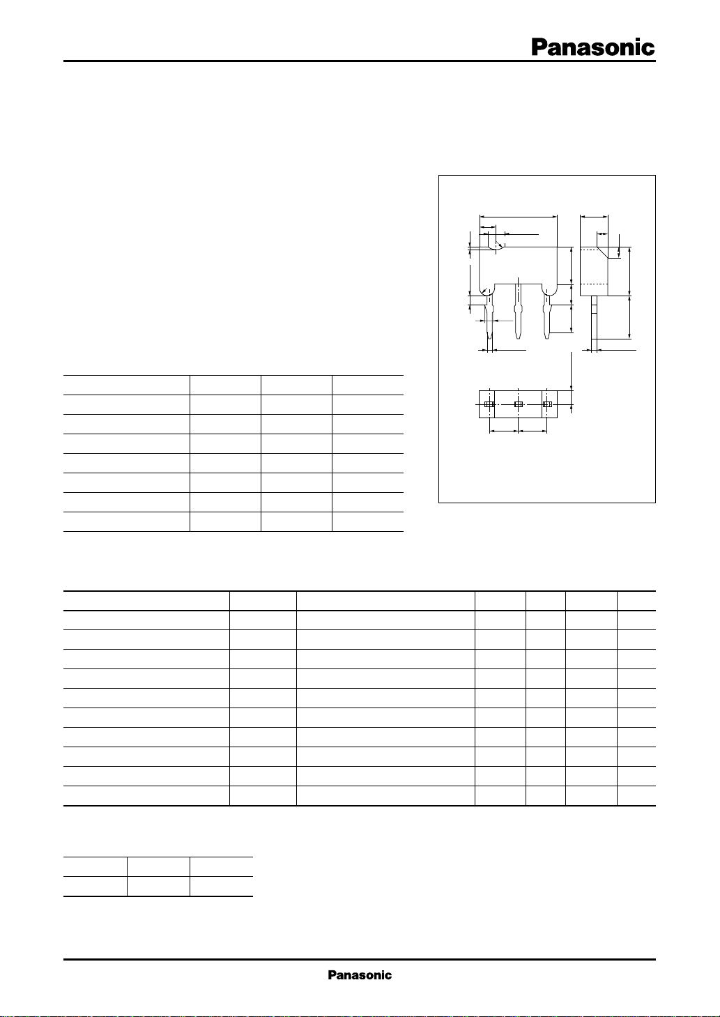
1:Base
2:Collector EIAJ:SC–71
3:Emitter M Type Mold Package
min
typ
2.5±0.1
3.5±0.1
2.0±0.2
2.4±0.21.25±0.05
123
max
30
20
5
70
220
0.1
0.7
150
300
2.8
4
1.5
50
Unit: mm
1.0
1.0
4.1±0.2 4.5±0.1
Unit
V
V
V
V
V
MHz
dB
pF
Ω
*
hFE Rank classification
Rank B C
h
FE
70 ~ 140 110 ~ 220
1
Page 2
Transistor 2SC2206
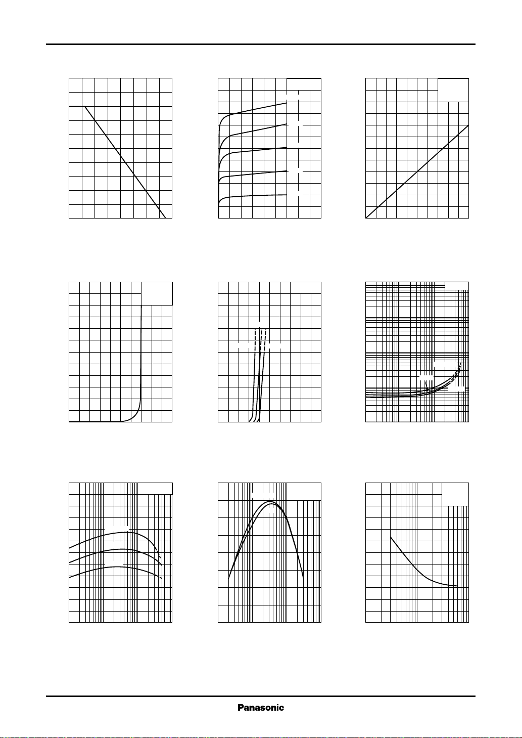
PC — Ta IC — V
500
)
450
mW
(
400
C
350
300
250
200
150
100
50
Collector power dissipation P
0
0 16040 12080 14020 10060
Ambient temperature Ta (˚C
IB — V
BE
120
100
)
µA
(
80
B
60
40
Base current I
20
0
01.00.80.2 0.60.4
Base to emitter voltage VBE (V
VCE=10V
Ta=25˚C
CE
12
10
)
mA
(
8
C
6
4
Collector current I
2
0
018612
)
Collector to emitter voltage VCE (V
IC — V
60
50
)
mA
)
(
40
C
30
20
Collector current I
10
0
0 2.01.60.4 1.20.8
Base to emitter voltage VBE (V
25˚C
Ta=75˚C
Ta=25˚C
IB=100µA
80µA
60µA
40µA
20µA
BE
VCE=10V
–25˚C
)
15.0
12.5
)
mA
(
10.0
C
7.5
5.0
Collector current I
2.5
0
0 1008020 6040
)
)
100
V
(
30
CE(sat)
10
3
1
0.3
0.1
0.03
0.01
Collector to emitter saturation voltage V
0.1 1 10 1000.3 3 30
IC — I
B
VCE=10V
Ta=25˚C
Base current IB (µA
V
— I
CE(sat)
C
IC/IB=10
Ta=75˚C
25˚C
–25˚C
Collector current IC (mA
)
)
hFE — I
C
240
FE
200
160
120
80
40
Forward current transfer ratio h
0
0.1 1 10 1000.3 3 30
Ta=75˚C
25˚C
–25˚C
Collector current IC (mA
2
VCE=10V
fT — I
E
400
350
)
MHz
300
(
T
250
200
150
100
Transition frequency f
50
0
– 0.1 –1 –10 –100– 0.3 –3 –30
)
VCB=10V
Emitter current IE (mA
Ta=25˚C
6V
)
60
)
Ω
(
50
rb
40
30
20
10
Reverse transfer impedance Z
0
– 0.1 – 0.3 –1 –3 –10
Zrb — I
E
VCB=10V
f=2MHz
Ta=25˚C
Emitter current IE (mA
)
Page 3

Transistor
2SC2206
Cre — V
)
3.0
pF
(
re
2.5
2.0
1.5
1.0
0.5
Common emitter reverse transfer capacitance C
0
0.1 1 10 1000.3 3 30
Collector to emitter voltage VCE (V
24
20
)
mS
(
16
ie
12
8
Input susceptance b
4
0
0403282416
IC=3mA
1mA
–2mA
=–1mA
E
I
f=10.7MHz
Input conductance gie (mS
bie — g
–4mA
58
CE
ie
–7mA
100
f=10.7MHz
Ta=25˚C
yie=gie+jb
VCE=10V
)
ie
10– 0.1
)
PG — I
E
24
20
f=100MHz
V
=10V
CE
Ta=25˚C
)
dB
(
16
12
8
Power gain PG
4
0
– 0.1 –1 –10 –100– 0.3 –3 –30
Emitter current IE (mA
bre — g
0
)
yre=gre+jb
re
VCE=10V
mS
(
re
– 0.2
– 0.3
– 0.4
– 0.5
Reverse transfer susceptance b
– 0.6
– 0.5 0– 0.1– 0.4 – 0.2– 0.3
)
re
f=10.7MHz
IE=–1mA
58
100
Reverse transfer conductance gre (mS
NF — I
E
12
10
)
dB
(
8
6
4
Noise figure NF
2
0
– 0.1 – 0.3 –1 –3 –10
Emitter current IE (mA
bfe — g
fe
0
)
– 0.1mA
mS
(
–20
fe
–40
–60
–80
–100
Forward transfer susceptance b
–120
0 1008020 6040
)
Forward transfer conductance gfe (mS
–1mA
–2mA
100
IE=–4mA
100
f=10.7MHz
58
100
58
VCB=6V
f=100MHz
R
=50Ω
g
Ta=25˚C
10.7
58
yfe=gfe+jb
VCE=10V
)
fe
)
boe — g
1.2
)
1.0
mS
(
oe
0.8
IE=–1mA
100
0.6
58
0.4
0.2
Output susceptance b
f=10.7MHz
0
00.50.40.1 0.30.2
Output conductance goe (mS
oe
yoe=goe+jb
VCE=10V
oe
)
3
 Loading...