

Page 1
2N7002W
60V N-Channel Enhancement Mode MOSFET
FEATURES
• R
, VGS@10V,IDS@500mA=5Ω
DS(ON)
• R
, VGS@4.5V,IDS@75mA=7.5Ω
DS(ON)
• Advanced Trench Process Technology
• High Density Cell Design For Ultra Low On-Resistance
• Specially Designed for Battery Operated Systems, Solid-State Relays
Drivers : Relays, Displays, Lamps, Solenoids, Memories, etc.
• Lead free in comply with EU RoHS 2002/95/EC directives.
• Green molding compound as per IEC61249 Std. . (Halogen Free)
MECHANICAL DATA
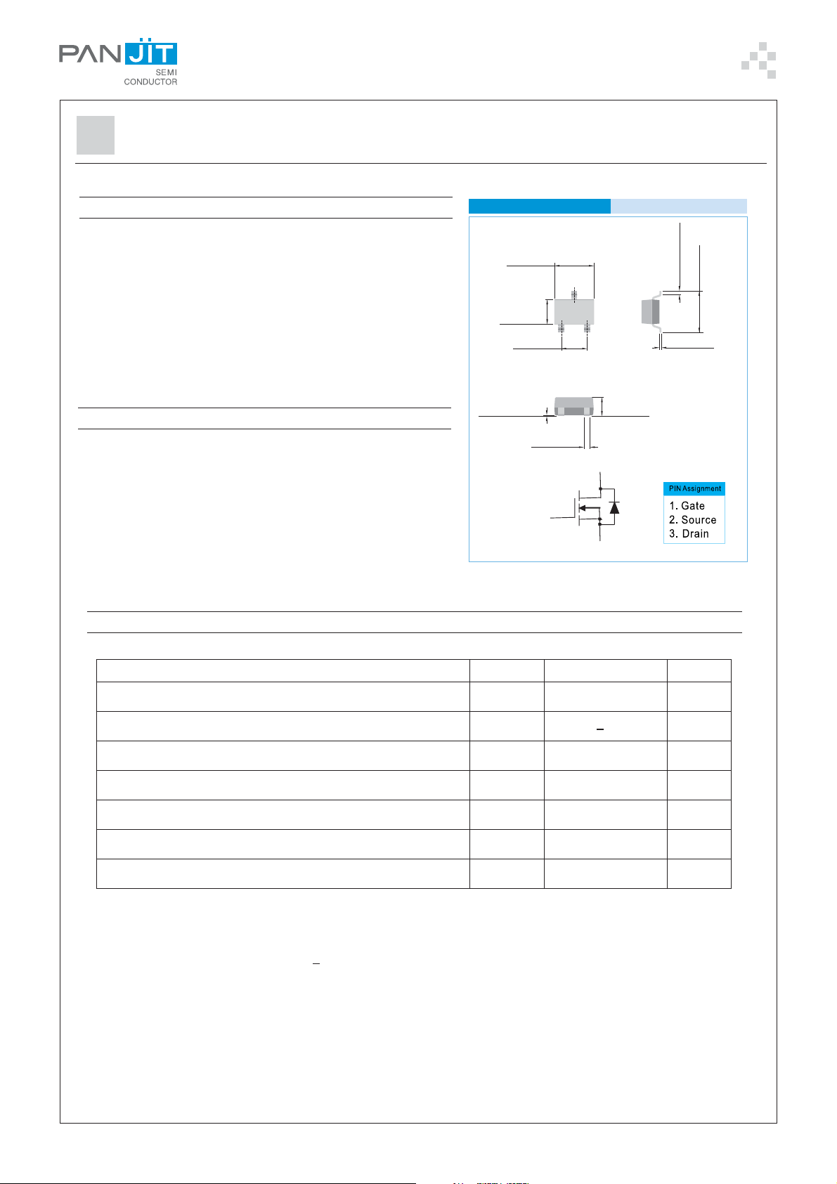
• Case: SOT-323 Package
• Terminals : Solderable per MIL-STD-750,Method 2026
• Apporx. Weight: 0.0002 ounces, 0.005 grams
• Marking : 72W
SOT-323
0.087(2.20)
0.070(1.80)
0.054(1.35)
0.045(1.15)
0.056(1.40)
0.047(1.20)
0.004(0.10)MAX.
0.016(0.40)
0.008(0.20)
Gate
Drain
Source
0.044(1.10)
0.035(0.90)
Unit inch(mm):
0.004(0.10)MIN.
0.087(2.20)
0.078(2.00)
0.006(0.15)
0.002(0.05)
Maximum RATINGS and Thermal Characteristics (TA=25OC unless otherwise noted )
RETEMARAPlobmyStimiLstinU
egatloVecruoS-niarD V
egatloVecruoS-etaG V
tnerruCniarDsuounitnoC I
)1
tnerruCniarDdesluP
noitapissiDrewoPmumixaM
2
)detnuomBCP(ecnatsiseRlamrehTtneibmAot-noitcnuJ
Note: 1. Maximum DC current limited by the package
2. Surface mounted on FR4 board, t < 10 sec
T
52=OC
A
TA57=OC
egnaRerutarepmeTegarotSdnanoitcnuJgnitarepO T
I
P
JT,GTS
R
SD
SG
D
MD
D
θ AJ
06V
+ 02V
511Am
008Am
002
021
051+ot55-
526
Wm
O
C
O
W/C
PAGE . 1STAD-JUL.26.2007
Page 2
2N7002W
ELECTRICAL CHARACTERISTICS
retemaraPlobmySnoitidnoCtseT.niM.pyT.xaMstinU
citatS
egatloVnwodkaerBecruoS-niarDVB
egatloVdlohserhTetaGV
ecnatsiseRetatS-nOecruoS-niarDR
SSD
)ht(SG
)no(SD
V
VSDV=SGI,
V
I,V0=
SG
SG
Au01=06--V
D
Au052=1-5.2V
D
I,V5.4=
Am57=--5.7
D
Ω
ecnatsiseRetatS-nOecruoS-niarDR
tnerruCniarDegatloVetaGoreZI
egakaeLydoBetaGI
ecnatcudnocsnarTdrawroFg
)no(SD
SSD
SSG
Sf
V
SG
V
VSG=+ V,V02
V
SD
I,V01=
Am005=--5
D
V,V06=
SD
V0=--1Au
SG
V0=--+001An
SD
I,V51=
Am052=002--Sm
D
cimanyD
egrahCetaGlatoTQ
egrahCniarD-etaGQ
emiTyaleDnO-nruTt
emiTyaleDffO-nruTt
g
sg
dg
no
ffo
V
I
D
I,V51=
SD
V
SG
V
DD
R
G
V,Am005=
D
01= Ω
Am005=
V5.4=
R,V01=
02= Ω
L
V01=
NEG
-6.07.0
-1.0-
CnegrahCecruoS-etaGQ
-80.0-
-951
sn
-1262
ecnaticapaCtupnIC
ecnaticapaCrefsnarTesreveRC
ssi
sso
ssr
V
V,V52=
SD
V0=
SG
HM0.1=f
Z
edoiDniarD-ecruoS
---052Am
V,Am052=
V0=-39.02.1V
SG
Switching
tnerruCdrawroFedoiD.xaMI
egatloVdrawroFedoiDV
s
DS
I
S
V
DD
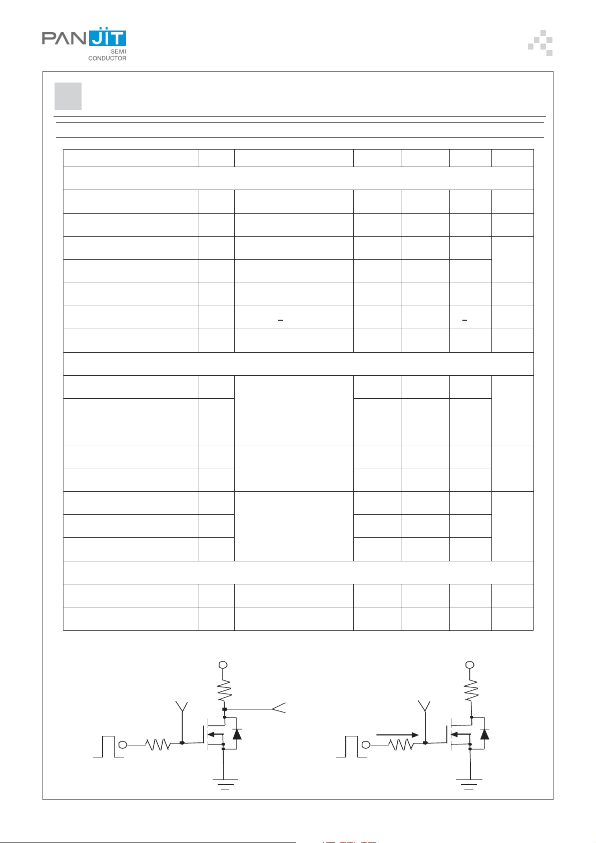
Test Circuit
R
V
IN
R
G
L
V
OUT
--05
--52
--5
Gate Charge
Test Circuit
1mA
FpecnaticapaCtuptuOC
V
DD
R
V
GS
R
G
L
PAGE . 2STAD-JUL.26.2007
Page 3
2N7002W
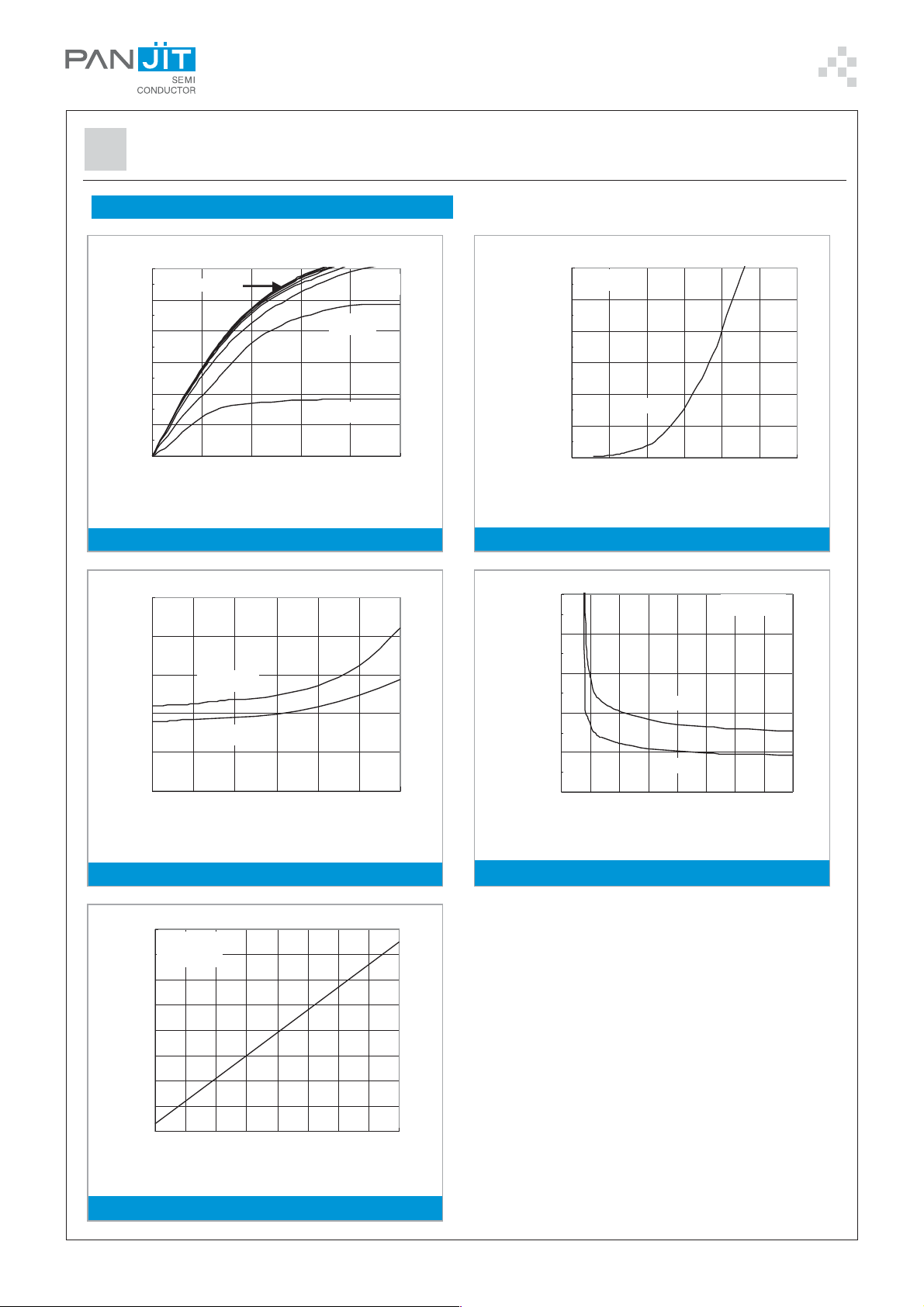
Typical Characteristics Curves (T =25 C,unless otherwise noted)
1.2
V = 10V ~ 6.0V
GS
1
0.8
0.6
0.4
0.2
- Drain-to-Source Current (A)
D
I
0
012345
O
A
5.0V
4.0V
3.0V
VDS- Drain-to-Source Voltage (V)
Fig. 1-TYPICAL FORWARD CHARACTERISTIC
FIG.1- Output Characteristic
5
W
4
1.2
V =10V
DS
V =10V
DS
V =10V
DS
1
0.8
0.6
0.4
0.2
- Drain Source Current (A)
D
I
0
0123456
O
T =25 C
J
VGS- Gate-to-Source Voltage (V)
FIG.2- Transfer Characteristic
10
W
8
I =500mA
D
3
2
1
DS(ON)
R - On-Resistance ( )
0
V =4.5V
GS
V =10V
GS
0 0.2 0.4 0.6 0.8 1 1.2
ID- Drain Current (A)
FIG.3- On Resistance vs Drain Current
2
V =10V
GS
1.8
I =500mA
D
1.6
1.4
1.2
1
0.8
- On-Resistance( Normalized)
0.6
DS(ON)
R
0.4
-50 -25 0 25 50 75 100 125 150
TJ- Junction Temperature (oC)
6
O
T =125 C
4
2
DS(ON)
R - On-Resistance ( )
0
2345678910
V
GS
J
O
T =25 C
J
- Gate -t o-Sour ce Voltage (V )
FIG.4- On Resistance vs Gate to Source Voltage
FIG.5- On Resistance vs Junction Temperature
PAGE . 3STAD-JUL.26.2007
Page 4

2N7002W
Vgs
Vgs(th)
Qg(th)
Qg
Qsw
QgdQgs
Qg
10
V =15V
DS
I =500mA
D
8
6
4
2
- Gate-to-Source Voltag e (V)
GS
V
0
0 0.2 0.4 0.6 0.8 1
Qg-GateCharge(nC)
Fig.6 - Gate Charge Waveform
1.2
1.1
1
0.9
0.8
0.7
- G-S Threshold Voltage (NORMALIZED)
th
0.6
V
-50 -25 0 25 50 75 100 125 150
TJ- Junction Temperature (oC)
I =250uA
D
Fig.8 - Threshold Voltage vs Temperature
10
V =0V
GS
Fig.7 - Gate Charge
73
I =250uA
D
72
71
70
69
68
67
66
- Breakdown Voltage (V)
65
DSS
64
BV
-50 -25 0 25 50 75 100 125 150
TJ- Junction Temperature (oC)
Fig.9 - Breakdown Voltage vs Junction Temperature
1
T =125 C
0.2 0.4 0.6 0.8 1 1.2 1.4 1.6 1.8
- Source Cur rent (A)
S
I
0.1
0.01
T =25 C
J
J
O
O
O
T =-55 C
J
VSD- Source-to-Drain Voltage (V)
Fig.10 - Source-Drain Diode Forward Voltage
PAGE . 4STAD-JUL.26.2007
Page 5

2N7002W
MOUNTING P AD LA YOUT
SOT-323
0.034
(0.86)
0.026
(0.65)
0.026
(0.66)
0.026
(0.65)
Unit inch(mm):
0.073
(1.85)
ORDER INFORMA TION
• Packing information
T/R - 12K per 13" plastic Reel
T/R - 3K per 7” plastic Reel
LEGAL ST ATEMENT
Copyright PanJit International, Inc 2012
The information presented in this document is believed to be accurate and reliable. The specifications and information herein
are subject to change without notice. Pan Jit makes no warranty, representation or guarantee regarding the suitability of its
products for any particular purpose. Pan Jit products are not authorized for use in life support devices or systems. Pan Jit
does not convey any license under its patent rights or rights of others.
STAD-JUL.26.2007
PAGE . 5
Page 6

2N7002W
For example :
RB500V-40_R2_00001
Part No.
Packing Code XX Vers i on Code XXXXX
Serial number
Version code means HF
Packing size code means 13"
Packing type means T/R
Packing
type
st
1
Code
Packing
size code
T/B A N/A 0 HF 0 se r ia l nu m b er
T/R R 7" 1 RoHS 1 se r ia l nu m b er
B/P B 13" 2
T/P T 26mm X
TRR S 52mm Y
TRL L PBCU U
FORMING F PBCD D
Part No_packing code_Version
2N7002W_R1_00001
2N7002W_R2_00001
nd
2
Code HF or RoHS 1st Code 2nd~5
th
Code
STAD-JUL.26.2007
PAGE . 6
Page 7

 Loading...