

Page 1
2N7002KTB
0.013(0.33)0.009(0.23
)
0. 024 (0. 60)
0. 019 (0. 50)
60V N-Channel Enhancement Mode MOSFET - ESD Protected
FEATURES
• R
, VGS@10V,IDS@500mA=3
DS(ON)
• R
, VGS@4.5V,IDS@200mA=4
DS(ON)
• Advanced Trench P rocess Technology
• High Density Cell Design For Ultra Low On-Resistance
• Very Low Leakage Current In Off Condition
• Specially Designed for Battery Operated Systems, Solid-State Relays
Drivers : Relays, Displays, Lamps, Solenoids, Memories, etc.
• ESD Protected 2KV HBM
• Lead free in comply with EU RoHS 2002/95/EC directives.
• Green molding compound as per IEC61249 Std. . (Halogen Free)
MECHANICAL DATA
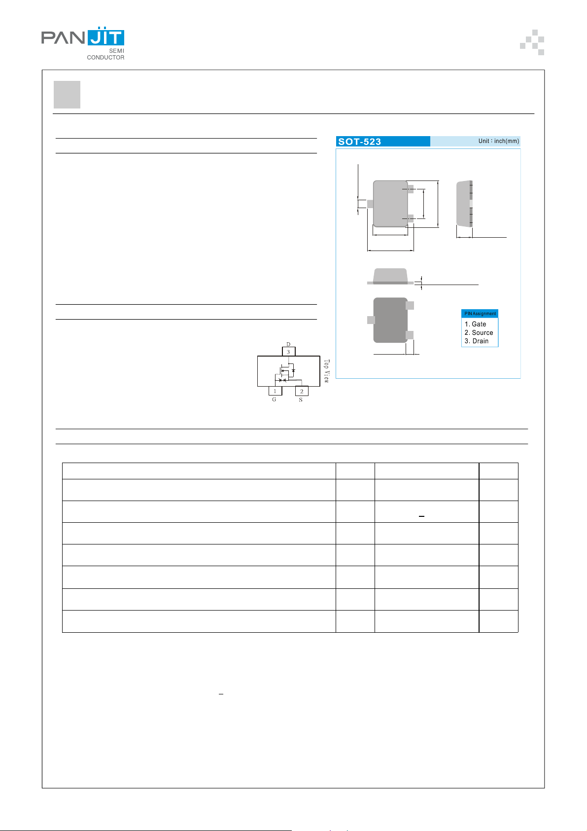
• Case: SOT-523 Package
• Terminals : Solderable per MIL-STD-750,Method 2026
• Approx. Weight: 0.00007 ounces, 0.002 grams
• Marking : 27
0.0 52(1. 30)
0.0 43(1. 10)
0.0 67(1. 70)
0.0 59(1. 50)
0. 012 (0. 30)
0. 004 (0. 10)
0.0 44(1 .10)
0.0 35(0 .90)
0.0 67(1 .70 )
0.0 07(0. 17)
0.0 02(0. 07)
0.0 59(1 .50 )
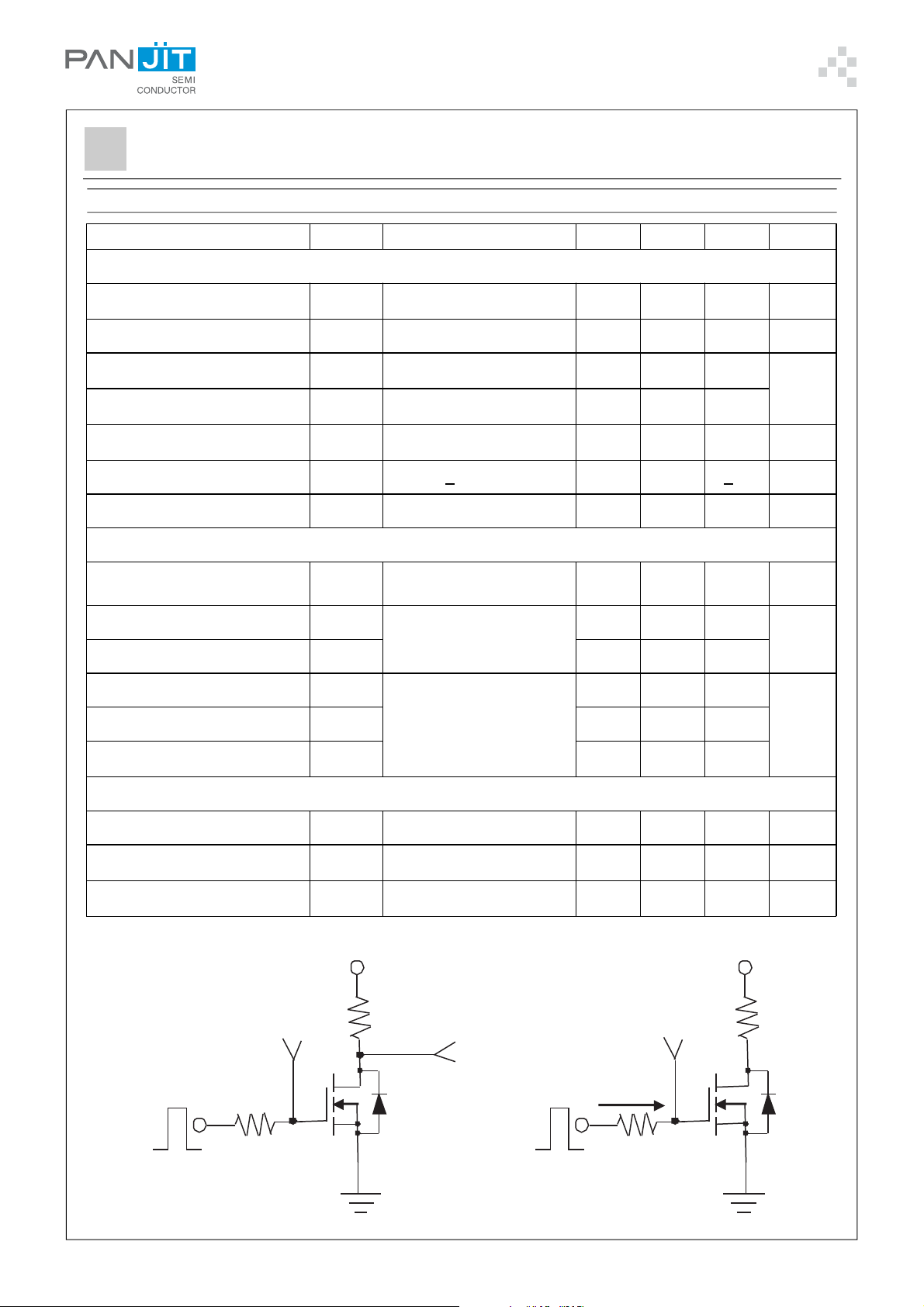
Maximum RATINGS and Thermal Characteristics (TA=25OC unless otherwise noted )
PA RA ME TE R S ymb o l Li m i t Uni ts
D r a i n - S o ur c e V o l t a g e V
Ga t e - S o u r c e Volta g e V
C o nt i nuo us D ra i n C ur r e nt I
P u ls e d D r a i n C u r r e nt
Ma xi mu m P o we r Di ss i pa t i o n
1)
TA=2 5OC
TA=7 5OC
Op e r a ti ng J un c t i on a nd St o ra g e Temp e r ature Ra n g e TJ,T
Junction-to Ambient Thermal Resistance(PCB mounted)
Note: 1. Maximum DC current limited by the package
2. Surface mounted on FR4 board, t < 5 sec
2
DS
GS
D
I
D M
P
D
ST G
R
J A
-5 5 t o + 15 0
6 0 V
+2 0 V
11 5 mA
8 0 0 mA
2 0 0
1 5 0
8 8 3
mW
O
O
C / W
C
PAGE . 1July 20,2012-REV.02
Page 2
2N7002KTB
ELECTRICAL CHARACTERISTICS
P a ra m e ter S ym b o l Tes t C on d i t i o n Mi n . Typ . Ma x. Uni t s
S t a ti c
D r a i n - S ourc e B re a k d o wn
Vo l ta g e
B V
Ga t e Thre s h o l d V o lt ag e V
D r a i n - S ourc e O n- S tat e
Re s i st a nc e
D r a i n - S ourc e O n- S tat e
Re s i st a nc e
Ze r o Ga t e V o lta g e D ra i n
C u r r e nt
R
R
I
Gate Body Leakage I
Forward Transconductance g
Dynamic
Tota l G a te C h a r g e Q
Turn- O n D e la y Ti m e td
Turn- O f f D ela y Ti m e td
Inp ut C ap a c i t a nc e C
Out p ut C a p ac i ta n c e C
Re ve r s e Tra nsfe r
C a p a c it a nc e
C
D SS
GS (t h)
DS (o n)
DS (o n)
D SS
GS S
fS
g
(o n)
(o ff)
i ss
o ss
rs s
VGS=0 V, ID=1 0 A 6 0 - - V
VDS=VGS, ID=2 5 0 A 1 - 2 .5 V
VGS=4.5V, I D=200mA - - 4 . 0
VGS=10V, I D=500mA - - 3.0
VDS=60V, VGS=0V - - 1 A
VGS=+2 0 V, VDS=0 V - - +1 0 A
VDS=1 5 V, ID=2 5 0m A 1 0 0 - - m S
VDS=1 5 V, ID=2 0 0m A
VGS=4.5V
VDD=30V , RL=150
ID=200mA , V
RG=10
GEN
=10V
- - 0 .8 n C
- - 20
ns
- - 1 25
- - 3 5
VDS=2 5 V, VGS=0 V
f=1 . 0 M H
Z
- - 10
p F
- - 5
S o urc e - D ra i n D io d e
D i o d e F o r wa rd Vo l t a g e V
C o nti nuo us D i o d e F or wa rd
C u r r e nt
P ul s e d D i o d e F o r wa rd
C u r r e nt
Switching
Test Circuit
V
IN
R
G
SD
I
s
I
sM
IS=2 0 0m A , VGS=0 V - 0 . 8 2 1 .3 V
- - - 11 5 mA
- - - 800 m A
V
DD
Gate Charge
V
DD
Test Circuit
R
L
V
OUT
V
GS
1mA
R
G
R
L
PAGE . 2July 20,2012-REV.02
Page 3
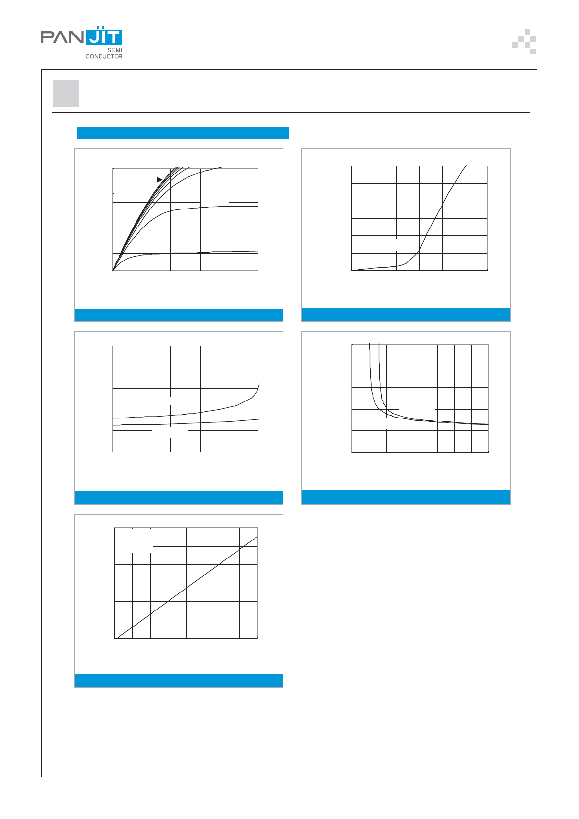
FIG.1- Output Characteristic
Typical Characteristics Curves (T =25 C,unless otherwise noted)
A
O
FIG.2- Transfer Characteristic
FIG.3- On Resistance vs Drain Current
FIG.4- On Resistance vs Gate to Source Voltage
FIG.5- On Resistance vs Junction Temperature
0
0.2
0.4
0.6
0.8
1
1.2
012345
VDS- Drain-to-Source Voltage (V)
I
D
- Drain-to-Source Current (A)
VGS= 6.0~10V
5.0V
4.0V
3.0V
0
1
2
3
4
5
2345678910
V
GS
- Gate -to -Source Voltage (V)
ID=200mA
ID=500mA
0
1
2
3
4
5
0 0.2 0.4 0 .6 0.8 1
ID-DrainCurrent(A)
VGS=4.5V
VGS=10V
0.6
0.8
1
1.2
1.4
1.6
1.8
-50 -25 0 25 50 75 100 125 150
TJ- Junction Temperature (oC)
R
DS(ON)
- On- Resistance(Normalized)
VGS=10V
I
D
=500mA
2N7002KTB
Typical Characteristics Curves (T =25 C,unless otherwise noted)
O
A
5.0V
4.0V
3.0V
Fig. 1-TYPICAL FORWARD CHARACTERISTIC
FIG.1- Output Characteristic
W
1.2
V =10V
DS
V =10V
DS
V =10V
DS
1
0.8
0.6
0.4
T =25
J
℃
T =25
J
℃
T =25
J
0.2
- Drain Source Current (A)
D
I
0
0123456
℃
VGS- Gate-to-Source Voltage (V)
FIG.2- Transfer Characteristic
W
DS(ON)
R - On-Resistance ( )
FIG.3- On Resistance vs Drain Current
July 20,2012-REV.02
FIG.5- On Resistance vs Junction Temperature
I =200mA
D
DS(ON)
R - On-Resistance ( )
FIG.4- On Resistance vs Gate to Source Voltage
PAGE . 3
Page 4

Fig.7 - Gate Charge
Fig.9 - Breakdown Voltage vs Junction Temperature
72
74
76
78
80
82
84
86
88
-50 -25 0 25 50 75 100 125 150
TJ- Junction Temperature (oC)
BV
DSS
- Breakdown Voltage (V)
ID = 250uA
2N7002KTB
Vgs
Vgs(th)
Qg(th)
Qg
Qsw
10
V =10V
DS
I =250mA
D
8
6
4
2
- Gate-to-Source Voltage (V)
GS
V
0
0 0.2 0.4 0.6 0.8 1
QgdQgs
Qg
Qg-GateCharge(nC)
Fig.6 - Gate Charge WaveformFig.6 - Gate Charge Waveform
1.2
1.1
1
0.9
0.8
- G-S Threshold Voltage (NORMALIZED)
th
0.7
V
-50 -25 0 25 50 75 100 125 150
TJ- Junction Temperature (oC)
ID=250mA
Fig.8 - Threshold Voltage vs TemperatureFig.8 - Threshold Voltage vs Temperature
10
V =0V
GS
1
25
-55
℃
℃
0.1
T =125
J
- Source Current (A)
S
I
0.01
0.2 0.4 0.6 0.8 1 1.2 1.4 1.6
℃
VSD- Source-to-Drain Voltage (V)
Fig.7 - Gate Charge
Fig.9 - Breakdown Voltage vs Junction Temperature
Fig.10 - Source-Drain Diode Forward VoltageFig.10 - Source-Drain Diode Forward Voltage
July 20,2012-REV.02
PAGE . 4
Page 5

2N7002KTB
MOUNTING PAD LAYOUT
SOT-523
0.053
(1.35)
0.019
(0.50)
0.016
(0.40)
0.019
(0.50)
0.017
(0.45)
Unit inch(mm):
ORDER INFORMATION
• Packing information
T/R - 4K per 7" plastic Reel
July 20,2012-REV.02
PAGE . 5
Page 6

2N7002KTB
Part No_packing code_Version
2N7002KTB_R1_00001
For example :
RB500V-40_R2_00001
Serial number
Part No.
Version code means HF
Packing size code means 13"
Packing type means T/R
Packing type 1st Code Packing size code 2nd Code HF or RoHS 1st Code 2nd~5
Tape and Ammunition Box
(T/B)
Tape and Reel
(T/R)
Bulk Packing
(B/P)
Tube Packing
(T/P)
Tape and Reel (Right Oriented)
(TRR)
Tape and Reel (Left Oriented)
(TRL)
FORMING F
Packing Code XX Version Code XXXXX
th
Code
A N/A 0 HF 0 serial number
R 7" 1 RoHS 1 serial number
B 13" 2
T 26mm X
S 52mm Y
L
PANASERT T/B CATHODE UP
(PBCU)
PANASERT T/B CATHODE DOWN
(PBCD)
U
D
July 20,2012-REV.02
PAGE . 6
Page 7

2N7002KTB
Disclaimer
z Reproducing and modifying information of the document is prohibited without
permission from Panjit International Inc..
z Panjit International Inc. reserves the rights to make changes of the content herein the
document anytime without notification. Please refer to our website for the latest
document.
z Panjit International Inc. disclaims any and all liability arising out of the application or
use of any product including damages incidentally and consequentially occurred.
z Panjit International Inc. does not assume any and all implied warranties, including
warranties of fitness for particular purpose, non-infringement and merchantability.
z Applications shown on the herein document are examples of standard use and
operation. Customers are responsible in comprehending the suitable use in particular
applications. Panjit International Inc. makes no representation or warranty that such
applications will be suitable for the specified use without further testing or modification.
z The products shown herein are not designed and authorized for equipments requiring
high level of reliability or relating to human life and for any applications concerning
life-saving or life-sustaining, such as medical instruments, transportation equipment,
aerospace machinery et cetera. Customers using or selling these products for use in
such applications do so at their own risk and agree to fully indemnify Panjit
International Inc. for any damages resulting from such improper use or sale.
July 20,2012-REV.02
PAGE . 7
Page 8

 Loading...