

Page 1

2N7002F
N-channel TrenchMOS FET
Rev. 03 — 28 April 2006 Product data sheet
1. Product profile
1.1 General description
N-channel enhancement mode Field-Effect Transistor (FET) in a plastic package using
TrenchMOS technology.
1.2 Features
■ Logic level threshold compatible ■ Very fast switching
■ Surface-mounted package ■ TrenchMOS technology
1.3 Applications
■ Logic level translator ■ High-speed line driver
1.4 Quick reference data
■ VDS≤ 60 V ■ ID≤ 475 mA
■ R
≤ 2 Ω ■ P
DSon
≤ 0.83 W
tot
2. Pinning information
Table 1: Pinning
Pin Description Simplified outline Symbol
1 gate (G)
2 source (S)
3 drain (D)
12
3
SOT23
G
mbb076
D
S
Page 2
Philips Semiconductors
2N7002F
N-channel TrenchMOS FET
3. Ordering information
Table 2: Ordering information
Type number Package
Name Description Version
2N7002F TO-236AB plastic surface-mounted package; 3 leads SOT23
4. Limiting values
Table 3: Limiting values
In accordance with the Absolute Maximum Rating System (IEC 60134).
Symbol Parameter Conditions Min Max Unit
V
DS
V
DGR
V
GS
V
GSM
I
D
I
DM
P
tot
T
stg
T
j
Source-drain diode
I
S
I
SM
drain-source voltage 25 °C ≤ Tj≤ 150 °C - 60 V
drain-gate voltage (DC) 25 °C ≤ Tj≤ 150 °C; RGS=20kΩ -60V
gate-source voltage - ±30 V
peak gate-source voltage tp≤ 50 µs; pulsed; duty cycle = 25 % - ±40 V
drain current Tsp=25°C; VGS= 10 V; see Figure 2 and 3 - 475 mA
= 100 °C; VGS= 10 V; see Figure 2 - 300 mA
T
sp
peak drain current Tsp=25°C; pulsed; tp≤ 10 µs; see Figure 3 - 1.9 A
total power dissipation Tsp=25°C; see Figure 1 - 0.83 W
storage temperature −65 +150 °C
junction temperature −65 +150 °C
source current Tsp=25°C - 475 mA
peak source current Tsp=25°C; pulsed; tp≤ 10 µs - 1.9 A
2N7002F_3 © Koninklijke Philips Electronics N.V. 2006. All rights reserved.
Product data sheet Rev. 03 — 28 April 2006 2 of 12
Page 3
Philips Semiconductors
2N7002F
N-channel TrenchMOS FET
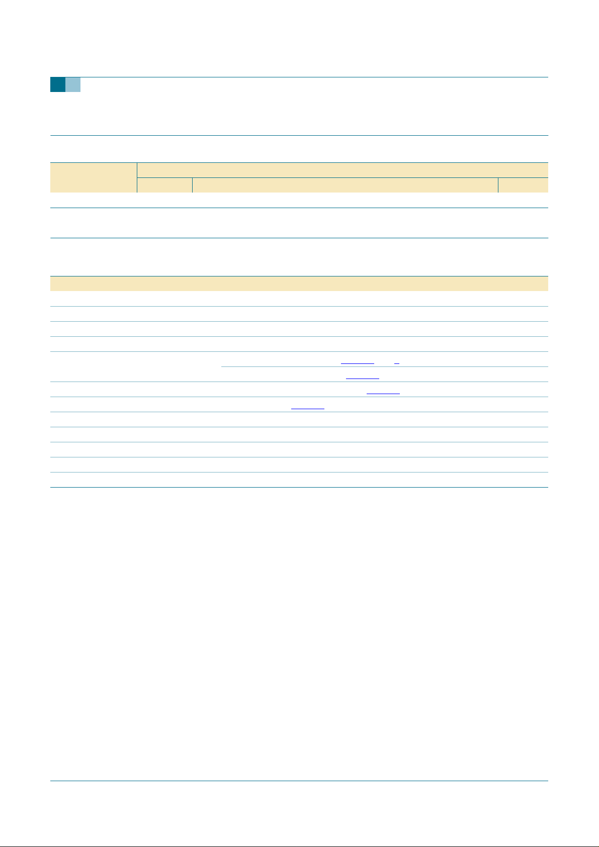
120
P
der
(%)
80
40
0
0 50 100 150 200
P
tot
P
der
------------------------
P
tot 25 C°()
100 %×= I
03aa17
T
(°C)
sp
Fig 1. Normalized total power dissipation as a
function of solder point temperature
10
120
I
der
(%)
80
40
0
0 50 100 150 200
I
D
der
-------------------- -
I
D25 C
()
100 %×=
°
03aa25
T
(°C)
sp
Fig 2. Normalized continuous drain current as a
function of solder point temperature
03ai11
I
D
(A)
1
-1
10
-2
10
1 10 10
Limit R
DSon
= V
/ I
DS
D
tp =
10 µs
100 µs
DC
VDS (V)
1 ms
10 ms
100 ms
Tsp=25°C; IDM is single pulse
Fig 3. Safe operating area; continuous and peak drain currents as a function of drain-source voltage
2
2N7002F_3 © Koninklijke Philips Electronics N.V. 2006. All rights reserved.
Product data sheet Rev. 03 — 28 April 2006 3 of 12
Page 4
Philips Semiconductors
2N7002F
N-channel TrenchMOS FET
5. Thermal characteristics
Table 4: Thermal characteristics
Symbol Parameter Conditions Min Typ Max Unit
R
th(j-sp)
R
th(j-a)
[1] Mounted on a printed-circuit board; minimum footprint; vertical in still air
thermal resistance from junction to solder point see Figure 4 - - 150 K/W
thermal resistance from junction to ambient
[1]
- - 350 K/W
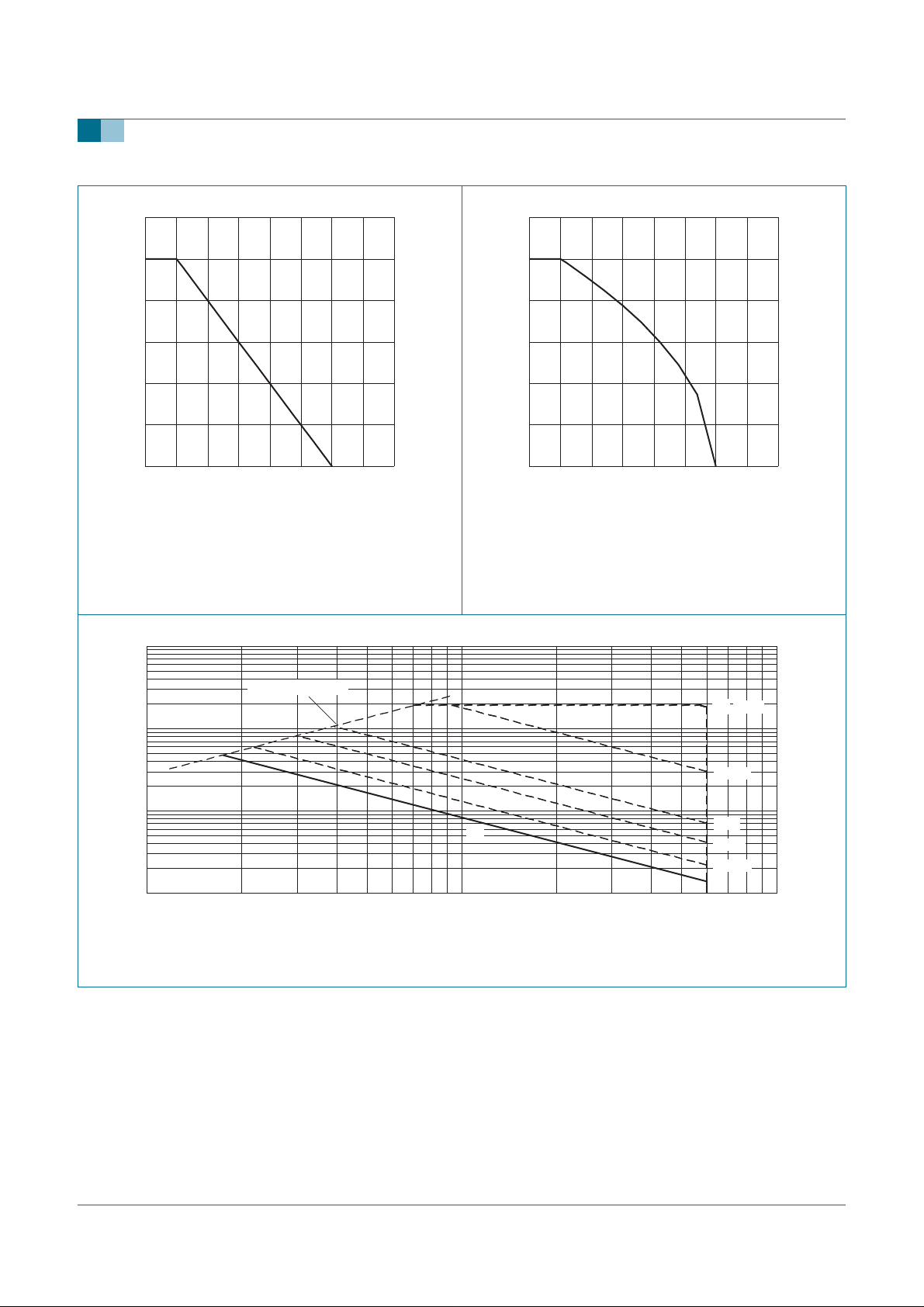
3
10
Z
th(j-sp)
(K/W)
2
10
δ =
0.5
0.2
0.1
10
0.05
0.02
single pul se
1
-5
10
-4
10
-3
10
-2
10
-1
10
1 10
t
(s)
p
Fig 4. Transient thermal impedance from junction to solder point as a function of pulse duration
003aab358
2N7002F_3 © Koninklijke Philips Electronics N.V. 2006. All rights reserved.
Product data sheet Rev. 03 — 28 April 2006 4 of 12
Page 5

Philips Semiconductors
2N7002F
N-channel TrenchMOS FET
6. Characteristics
Table 5: Characteristics
Tj=25°C unless otherwise specified.
Symbol Parameter Conditions Min Typ Max Unit
Static characteristics
V
(BR)DSS
drain-source breakdown
voltage
V
I
DSS
I
GSS
R
GS(th)
DSon
gate-source threshold voltage ID= 0.25 mA; VDS=VGS; see Figure 9 and 10
drain leakage current VDS=48V; VGS=0V
gate leakage current VGS= ±15 V; VDS= 0 V - 10 100 nA
drain-source on-state
resistance
Dynamic characteristics
Q
Q
Q
C
C
C
t
t
G(tot)
GS
GD
iss
oss
rss
on
off
total gate charge
gate-source charge - 0.1 - nC
gate-drain charge - 0.27 - nC
input capacitance VGS=0V; VDS= 10 V; f = 1 MHz;
output capacitance - 6.8 30 pF
reverse transfer capacitance - 3.5 10 pF
turn-on time VDS=50V; RL= 250 Ω; VGS=10V;
turn-off time - 11 15 ns
Source-drain diode
V
SD
t
rr
Q
r
source-drain voltage IS= 300 mA; VGS= 0 V; see Figure 13 - 0.85 1.5 V
reverse recovery time IS= 300 mA; dIS/dt = −100 A/µs; VGS=0V - 30 - ns
recovered charge - 30 - nC
ID=10µA; VGS=0V
=25°C 60--V
T
j
= −55 °C 55--V
T
j
=25°C 1 2 2.5 V
T
j
= 150 °C 0.6 - - V
T
j
= −55 °C - - 2.75 V
T
j
=25°C - 0.01 1 µA
T
j
= 150 °C --10µA
T
j
VGS= 10 V; ID= 500 mA; see Figure 6 and 8
=25°C - 0.78 2 Ω
T
j
= 150 °C - 1.45 3.7 Ω
T
j
= 4.5 V; ID= 75 mA; see Figure 6 and 8 - 1.2 4 Ω
V
GS
= 300 mA; VDS=30V; VGS=10V;
I
D
see
Figure 11 and 12
- 0.69 - nC
- 3150pF
see
Figure 14
- 2.5 10 ns
R
=50Ω; RGS=50Ω
G
2N7002F_3 © Koninklijke Philips Electronics N.V. 2006. All rights reserved.
Product data sheet Rev. 03 — 28 April 2006 5 of 12
Page 6

Philips Semiconductors
2N7002F
N-channel TrenchMOS FET
V
03ai13
DS
4.5
4
3.5VGS (V) =
(V)
1
I
D
(A)
0.8
0.6
0.4
0.2
0
0 0.5 1 1.5 2
10 5
Tj=25°CT
Fig 5. Output characteristics: drain current as a
function of drain-source voltage; typical values
03ai16
(A)
1
I
D
0.8
4.5
03ai15
(A)
I
D
5
10
5000
R
DSon
(mΩ)
4000
3000
2000
1000
0
0 0.2 0.4 0.6 0.8 1
=25°C
j
VGS (V) =
4
Fig 6. Drain-source on-state resistance as a function
of drain current; typical values
2.4
a
1.8
03aa28
0.6
0.4
0.2
0
0246
Tj = 150 °C
Tj=25°C and 150 °C; VDS>ID× R
25 °C
V
DSon
(V)
GS
Fig 7. Transfer characteristics: drain current as a
function of gate-source voltage; typical values
1.2
0.6
0
-60 0 60 120 180
R
DSon
=
a
------------------------------
R
DSon 25 C°()
T
(°C)
j
Fig 8. Normalized drain-source on-state resistance
factor as a function of junction temperature
2N7002F_3 © Koninklijke Philips Electronics N.V. 2006. All rights reserved.
Product data sheet Rev. 03 — 28 April 2006 6 of 12
Page 7

Philips Semiconductors
2N7002F
N-channel TrenchMOS FET
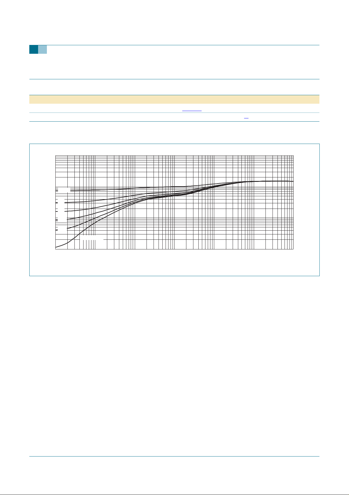
003aab101
V
GS(th)
3
max
(V)
2
1
0
-60 0 60 120 180
ID= 0.25 mA; VDS=V
typ
min
GS
T
(°C)
j
Fig 9. Gate-source threshold voltage as a function of
junction temperature
003aab359
V
(V)
10
GS
ID = 0.3 A
T
V
8
= 25 °C
j
= 30 V
DS
-3
10
I
D
003aab100
(A)
-4
10
-5
10
-6
10
0123
min typ max
V
(V)
GS
Tj=25°C; VDS=5V
Fig 10. Sub-threshold drain current as a function of
gate-source voltage
V
DS
6
4
2
0
0 0.2 0.4 0.6 0.8
(nC)
Q
G
ID= 300 mA; VDS=30V
Fig 11. Gate-source voltage as a function of gate
charge; typical values
I
D
V
GS(pl)
V
GS(th)
V
GS
Q
GS1QGS2
Q
G(tot)
Q
GD
003aaa508
Q
GS
Fig 12. Gate charge waveform definitions
2N7002F_3 © Koninklijke Philips Electronics N.V. 2006. All rights reserved.
Product data sheet Rev. 03 — 28 April 2006 7 of 12
Page 8

Philips Semiconductors
2N7002F
N-channel TrenchMOS FET
1
I
S
(A)
0.8
0.6
0.4
0.2
0
0.2 0.4 0.6 0.8 1
150 °C
03ai17
Tj = 25 °C
(V)
V
SD
Tj=25°C and 150 °C; VGS=0V VGS= 0 V; f = 1 MHz
Fig 13. Source current as a function of source-drain
voltage; typical values
03ai18
C
C
C
VDS (V)
iss
oss
rss
2
C
(pF)
10
10
1
2
-1
10
1 10 10
Fig 14. Input,output and reverse transfer capacitances
as a function of drain-source voltage; typical
values
2N7002F_3 © Koninklijke Philips Electronics N.V. 2006. All rights reserved.
Product data sheet Rev. 03 — 28 April 2006 8 of 12
Page 9

Philips Semiconductors
2N7002F
N-channel TrenchMOS FET
7. Package outline
Plastic surface-mounted package; 3 leads SOT23
D
3
A
A
1
12
e
1
b
p
e
w M
B
E
H
E
detail X
AB
Q
L
p
X
v M
A
c
0 1 2 mm
scale
DIMENSIONS (mm are the original dimensions)
A
UNIT
1.1
mm
0.9
OUTLINE
VERSION
SOT23 TO-236AB
1
A
max.
0.1
cD
b
p
0.48
0.15
0.38
0.09
IEC JEDEC JEITA
3.0
2.8
E
1.4
1.2
REFERENCES
1.9
e
e
0.95
HEL
1
2.5
2.1
0.45
0.15
Qwv
p
0.55
0.2
0.45
0.1
EUROPEAN
PROJECTION
ISSUE DATE
04-11-04
06-03-16
Fig 15. Package outline SOT23
2N7002F_3 © Koninklijke Philips Electronics N.V. 2006. All rights reserved.
Product data sheet Rev. 03 — 28 April 2006 9 of 12
Page 10

Philips Semiconductors
2N7002F
N-channel TrenchMOS FET
8. Revision history
Table 6: Revision history
Document ID Release date Data sheet status Change notice Doc. number Supersedes
2N7002F_3 20060428 Product data sheet - - 2N7002F_2
Modifications:
• Table 5 “Characteristics”: V
• Table 5 “Characteristics”: V
• Table 5 “Characteristics”: R
• Table 5 “Characteristics”: g
GS(th) ID
GS(th)
DSon
fs
• Table 5 “Characteristics”: Addition of Q
• Table 5 “Characteristics”: C
• Table 5 “Characteristics”: t
iss
on
• Figure 3, 4, 5, 6, 7, 9, 10, 13 and 14: modified
• Figure 11: added
2N7002F_2 20050509 Product data sheet - 9397 750 14945 2N7002F-01
2N7002F-01 20020211 Product data - 9397 750 09096 -
condition modified
maximum limits modified
typical values modified
removed
, QGS and Q
G(tot)
, C
and C
oss
and t
typical values modified
off
values modified
rss
GD
2N7002F_3 © Koninklijke Philips Electronics N.V. 2006. All rights reserved.
Product data sheet Rev. 03 — 28 April 2006 10 of 12
Page 11

Philips Semiconductors
9. Data sheet status
2N7002F
N-channel TrenchMOS FET
Level Data sheet status
I Objective data Development This data sheet contains data from the objective specification for product development. Philips
II Preliminary data Qualification Thisdata sheet containsdata from the preliminary specification.Supplementary datawill be published
III Product data Production This data sheet contains data from the product specification. Philips Semiconductors reserves the
[1] Please consult the most recently issued data sheet before initiating or completing a design.
[2] The product status of the device(s) described in this data sheet may have changed since this data sheet was published. The latest information is available on the Internet at
URL http://www.semiconductors.philips.com.
[3] For data sheets describing multiple type numbers, the highest-level product status determines the data sheet status.
[1]
Product status
10. Definitions
Short-form specification — The data in a short-form specification is
extracted from a full data sheet with the same type number and title. For
detailed information see the relevant data sheet or data handbook.
Limiting values definition — Limiting values given are in accordance with
the Absolute Maximum Rating System (IEC 60134). Stress above one or
more of the limiting values may cause permanent damage to the device.
These are stress ratings only and operation of the device at these or at any
other conditions above those given in the Characteristics sections of the
specification is not implied. Exposure to limiting values for extended periods
may affect device reliability.
Application information — Applications that are described herein for any
of these products are for illustrative purposes only. Philips Semiconductors
makes norepresentation or warrantythat such applicationswill be suitablefor
the specified use without further testing or modification.
[2] [3]
Definition
Semiconductors reserves the right to change the specification in any manner without notice.
at a laterdate.Philips Semiconductors reserves the right tochange the specification without notice, in
order to improve the design and supply the best possible product.
right to make changesatany time in order to improvethedesign, manufacturing and supply. Relevant
changes will be communicated via a Customer Product/Process Change Notification (CPCN).
customers using or selling these products for use in such applications do so
at their own risk and agree to fully indemnify Philips Semiconductors for any
damages resulting from such application.
Right to make changes — Philips Semiconductors reserves the right to
make changes in the products - including circuits, standard cells, and/or
software - described or contained herein in order to improve design and/or
performance. When the product is in full production (status ‘Production’),
relevant changes will be communicated via a Customer Product/Process
Change Notification (CPCN). Philips Semiconductors assumes no
responsibility or liability for the use of any of these products, conveys no
license or title under any patent, copyright, or mask work right to these
products, andmakes norepresentations or warrantiesthat these productsare
free frompatent, copyright, or maskwork right infringement, unless otherwise
specified.
12. Trademarks
11. Disclaimers
Life support — These products are not designed for use in life support
appliances, devices, or systems where malfunction of these products can
reasonably be expected to result in personal injury. Philips Semiconductors
Notice — All referenced brands, product names, service names and
trademarks are the property of their respective owners.
TrenchMOS —is a trademark of Koninklijke Philips Electronics N.V.
13. Contact information
For additional information, please visit: http://www.semiconductors.philips.com
For sales office addresses, send an email to: sales.addresses@www.semiconductors.philips.com
2N7002F_3 © Koninklijke Philips Electronics N.V. 2006. All rights reserved.
Product data sheet Rev. 03 — 28 April 2006 11 of 12
Page 12

Philips Semiconductors
14. Contents
1 Product profile . . . . . . . . . . . . . . . . . . . . . . . . . . 1
1.1 General description. . . . . . . . . . . . . . . . . . . . . . 1
1.2 Features . . . . . . . . . . . . . . . . . . . . . . . . . . . . . . 1
1.3 Applications . . . . . . . . . . . . . . . . . . . . . . . . . . . 1
1.4 Quick reference data. . . . . . . . . . . . . . . . . . . . . 1
2 Pinning information. . . . . . . . . . . . . . . . . . . . . . 1
3 Ordering information. . . . . . . . . . . . . . . . . . . . . 2
4 Limiting values. . . . . . . . . . . . . . . . . . . . . . . . . . 2
5 Thermal characteristics. . . . . . . . . . . . . . . . . . . 4
6 Characteristics. . . . . . . . . . . . . . . . . . . . . . . . . . 5
7 Package outline . . . . . . . . . . . . . . . . . . . . . . . . . 9
8 Revision history. . . . . . . . . . . . . . . . . . . . . . . . 10
9 Data sheet status . . . . . . . . . . . . . . . . . . . . . . . 11
10 Definitions . . . . . . . . . . . . . . . . . . . . . . . . . . . . 11
11 Disclaimers. . . . . . . . . . . . . . . . . . . . . . . . . . . . 11
12 Trademarks. . . . . . . . . . . . . . . . . . . . . . . . . . . . 11
13 Contact information . . . . . . . . . . . . . . . . . . . . 11
2N7002F
N-channel TrenchMOS FET
© Koninklijke Philips Electronics N.V. 2006
All rights are reserved. Reproduction in whole or in part is prohibited without the prior
written consent of the copyright owner. The information presented in this document does
not form part of any quotation or contract, is believed to be accurate and reliable and may
be changed without notice. No liability will be accepted by the publisher for any
consequence of its use. Publication thereof does not convey nor imply any license under
patent- or other industrial or intellectual property rights.
Published in The Netherlands
Date of release: 28 April 2006
Document number: 2N7002F_3
 Loading...