

Page 1
2N7002DW
60V N-Channel Enhancement Mode MOSFET
FEATURES
• R
, VGS@10V,IDS@500mA=5Ω
DS(ON)
• R
, VGS@4.5V,IDS@75mA=7.5Ω
DS(ON)
• Advanced Trench Process Technology
• High Density Cell Design For Ultra Low On-Resistance
• Specially Designed for Battery Operated Systems, Solid-State Relays
Drivers : Relays, Displays, Lamps, Solenoids, Memories, etc.
• /HDGIUHHLQFRPSO\ZLWK(85R+6(&GLUHFWLYHV
*UHHQPROGLQJFRPSRXQGDVSHU,(&6WG+DORJHQ)UHH
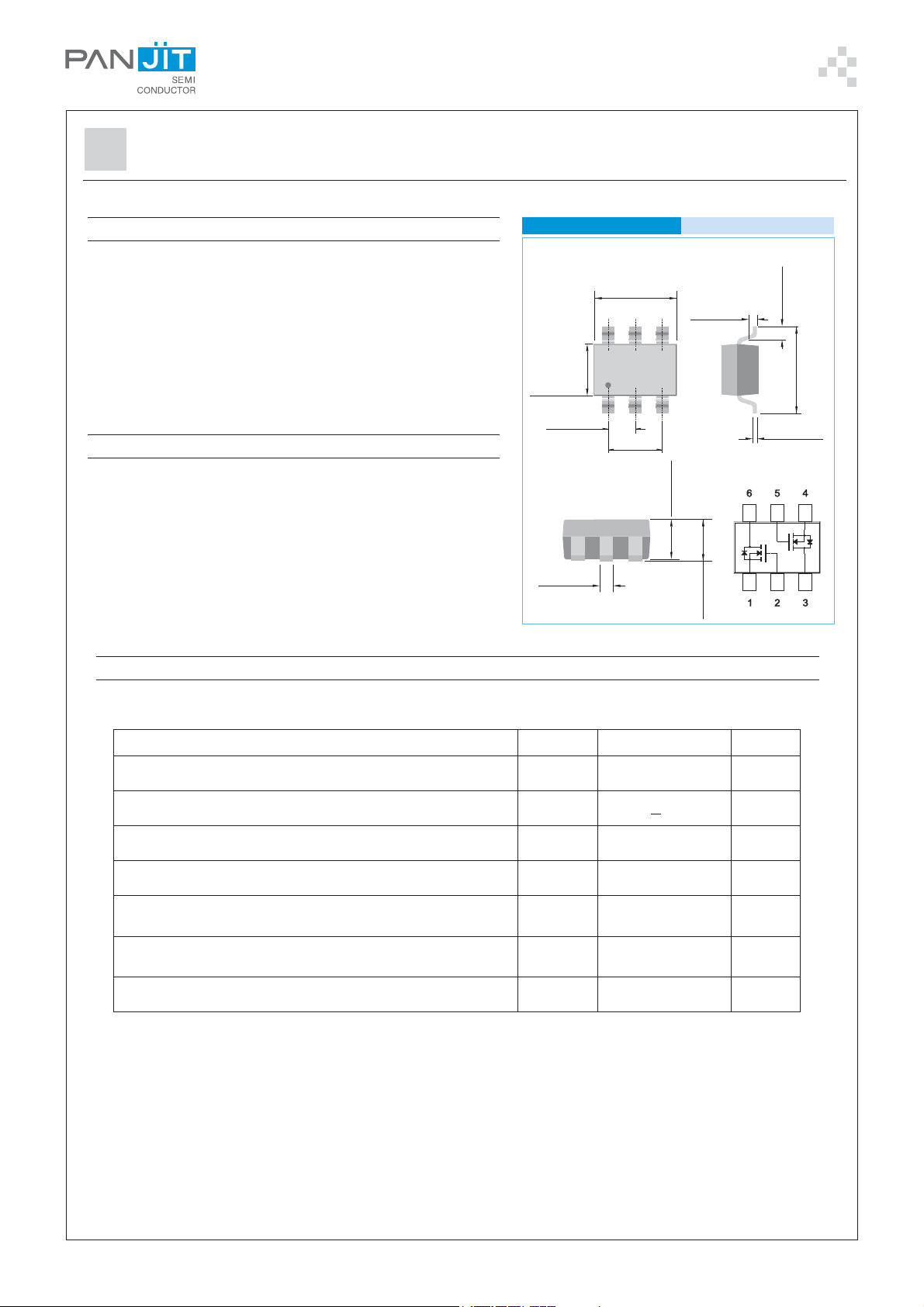
MECHANICAL DATA
• Case: SOT-363 Package
• Terminals : Solderable per MIL-STD-750,Method 2026
• Apporx. Weight: 0.0002 ounces , 0.006grams
• Marking : 702
SOT-363
0.054(1.35)
0.045(1.15)
0.030(0.75)
0.021(0.55)
0.012(0.30)
0.005(0.15)
0.087(2.20)
0.074(1.90)
0.056(1.40)
0.047(1.20)
0.010(0.25)
040(1.00)
031(0.80)
0.
0.
MAX.
0.044(1.10)
Unit inch(mm):
0.018(0.45)
0.006(0.15)
0.087(2.20)
0.010(0.25)
0.003(0.08)
0.078(2.00)
Maximum RATINGS and Thermal Characteristics (TA=25OC unless otherwise noted )
RETEMARAPlobmyStimiLstinU
egatloVecruoS-niarDV
egatloVecruoS-etaGV
tnerruCniarDsuounitnoCI
)1
tnerruCniarDdesluP
noitapissiDrewoPmumixaM
egnaR
Note: 1. Maximum DC current limited by the package
2. Surface mounted on FR4 board, t < 10 sec
52=OC
T
A
TA57=OC
erutarepmeTegarotSdnanoitcnuJgnitarepO
2
)detnuomBCP(ecnatsiseRlamrehTtneibmAot-noitcnuJ
T
D
I
P
JT,GTS
R
θ AJ
SD
SG
MD
D
06V
+ 02V
511Am
008Am
002
021
051+ot55-
526
Wm
O
C
O
W/C
PAN JIT RESERVES THE RIGHT TO IMPROVE PRODUCT DESIGN,FUNCTIONS AND RELIABILITY WITHOUT NOTICE
PAGE . 1REV.0.0-AUG.4.2008
Page 2
2N7002DW
ELECTRICAL CHARACTERISTICS
retemaraPlobmySnoitidnoCtseT.niM.pyT.xaMstinU
citatS
nwodkaerBecruoS-niarD
egatloV
VB
SSD
V
SG
I,V0=
Au01=06--V
D
egatloVdlohserhTetaGV
etatS-nOecruoS-niarD
ecnatsiseR
etatS-nOecruoS-niarD
ecnatsiseR
tnerruC
egakaeLydoBetaGI
ecnatcudnocsnarTdrawroFg
R
R
niarDegatloVetaGoreZ
I
SSD
SSG
Sf
)ht(SG
)no(SD
)no(SD
VSDV=
V
SG
V
SG
V
SD
VSG=+ V,V02
V
SD
SGI,D
I,V01=
Au052=1-5.2V
I,V5.4=
D
I,V51=
D
Am57=--5.7
D
Am005=--5
V,V06=
V0=--1Au
SG
V0=--+001An
SD
Am052=002--Sm
Ω
cimanyD
egrahCetaGlatoTQ
g
V
SD
I,V51=
D
VSGV5=
egrahCniarD-etaGQ
emiTyaleDnO-nruTt
emiTyaleDffO-nruTt
ecnaticapaCtupnIC
ecnaticapaCtuptuOC
refsnarTesreveR
ecnaticapaC
dg
V
no
ffo
ssi
sso
C
ssr
DD
I
D
V
SD
R,V01=
L
V,Am005=
R
01= Ω
G
V,V52=
HM0.1=f
Am005=
02= Ω
V01=
NEG
V0=
SG
Z
-6.07.0
CnegrahCecruoS-etaGQsg-1.0-
-80.0-
-951
sn
-1262
--05
--52
Fp
--5
tnerruC
Switching
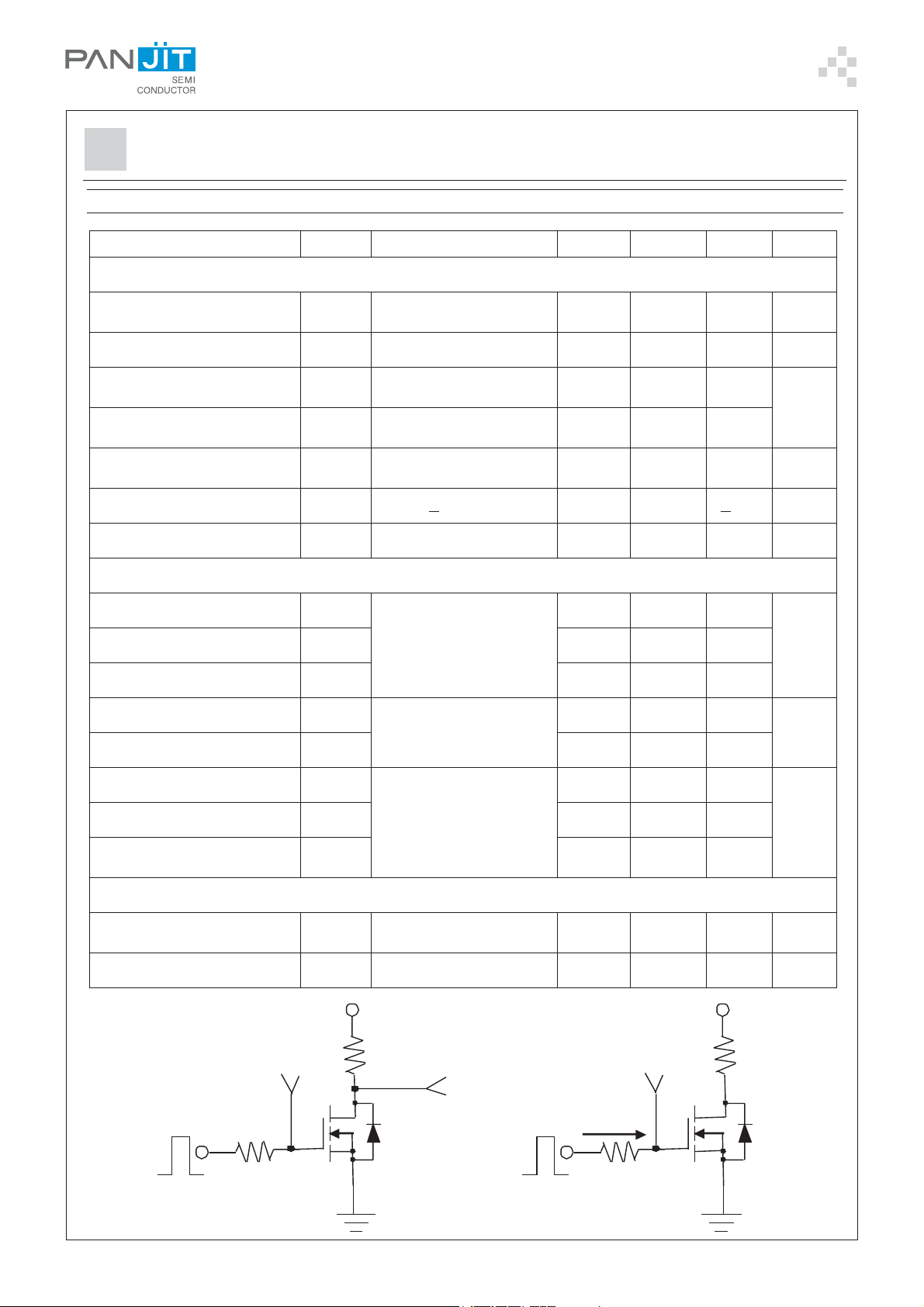
Test Circuit
edoiDniarD-ecruoS
drawroFedoiD.xaM
egatloVdrawroFedoiDV
I
s
DS
I
S
V
DD
---052Am
V,Am052=
SG
Gate Charge
Test Circuit
R
V
IN
R
G
L
V
OUT
V0=- 39.02.1V
V
DD
R
L
PAGE . 2REV.0.0-AUG.4.2008
1mA
R
V
GS
G
Page 3

2N7002DW
Typical Characteristics Curves (T =25 C,unless otherwise noted)
1.2
V = 10V ~ 6.0V
GS
1
0.8
0.6
0.4
0.2
- Drain-to-Source Current (A)
D
I
0
012345
O
A
5.0V
4.0V
3.0V
VDS- Drain-to-Source Voltage (V)
Fig. 1-TYPICAL FORWARD CHARACTERISTIC
FIG.1- Output Characteristic
5
W
4
1.2
V =10V
DS
V =10V
DS
V =10V
DS
1
0.8
0.6
0.4
0.2
- Drain Source Current (A)
D
I
0
0123456
O
T =25 C
J
VGS- Gate-to-Source Voltage (V)
FIG.2- Transfer Characteristic
10
W
8
I =500mA
D
3
2
1
DS(ON)
R - On-Resistance ( )
0
V =4.5V
GS
V =10V
GS
0 0.2 0.4 0.6 0.8 1 1.2
ID- Drain Current (A)
FIG.3- On Resistance vs Drain Current
2
V =10V
GS
1.8
I =500mA
D
1.6
1.4
1.2
1
0.8
- On-Resistance(Normalized)
0.6
DS(ON)
R
0.4
-50 -25 0 25 50 75 100 125 150
TJ- Junction Tempe rature (oC)
6
O
T =125 C
4
2
DS(ON)
R - On-Resistance ( )
0
2345678910
V
GS
J
O
T =25 C
J
- Gate -t o-Sour ce Voltage (V)
FIG.4- On Resistance vs Gate to Source Voltage
FIG.5- On Resistance vs Junction Temperature
PAGE . 3REV.0.0-AUG.4.2008
Page 4

2N7002DW
Vgs
Vgs(th)
Qg(th)
Qsw
Qg
QgdQgs
Qg
10
V =15V
DS
I =500mA
D
8
6
4
2
- Gate-t o-Source Voltage (V)
GS
V
0
0 0.2 0.4 0.6 0.8 1
Qg-GateCharge(nC)
Fig.6 - Gate Charge Waveform
1.2
1.1
1
0.9
0.8
0.7
- G-S Threshold Voltage (NORMALIZED)
th
0.6
V
-50 -25 0 25 50 75 100 125 150
TJ- Junction Tempe rature (oC)
I =250uA
D
Fig.8 - Threshold Voltage vs Temperature
10
V =0V
GS
Fig.7 - Gate Charge
73
I =250uA
D
72
71
70
69
68
67
66
- Breakdown Voltage (V)
65
DSS
64
BV
-50 -25 0 25 50 75 100 125 150
TJ- Junction Temperature (oC)
Fig.9 - Breakdown Voltage vs Junction Temperature
1
T =125 C
0.2 0.4 0.6 0.8 1 1.2 1.4 1.6 1.8
- Source C urrent (A )
S
I
0.01
0.1
T =25 C
J
J
O
O
O
T =-55 C
J
VSD- Source-to-Drain Voltage (V)
Fig.10 - Source-Drain Diode Forward Voltage
PAGE . 4REV.0.0-AUG.4.2008
Page 5

2N7002DW
MOUNTING PAD LAYOUT
SOT-363
0.020
(0.50)
0.018
(0.45)
0.026
(0.65)
0.026
(0.65)
Unit inch(mm):
0.075
(1.90)
ORDER INFORMATION
• Packing information
T/R - 10K per 13" plastic Reel
T/R - 3K per 7” plastic Reel
LEGAL STATEMENT
Copyright PanJit International, Inc 2012
The information presented in this document is believed to be accurate and reliable. The specifications and information herein
are subject to change without notice. Pan Jit makes no warranty, representation or guarantee regarding the suitability of its
products for any particular purpose. Pan Jit products are not authorized for use in life support devices or systems. Pan Jit
does not convey any license under its patent rights or rights of others.
REV.0.0-AUG.4.2008
PAGE . 5
Page 6

 Loading...