

Page 1
2N7002
N-CHANNEL ENHANCEMENT MODE FIELD EFFECT TRANSISTOR
VOL TAGE
60 V olts
CURRENT
115 mAmp
DESCRIPTION
• N-channel enhancement mode field effect transistor, designed for high speed pulsed
amplifier and driver applications, which is manufactored by the N-Channel DMOS
process.
FEATURES
• High density cell design for low RDS(ON).
• Voltage controlled small signal switching.
• Rugged and reliable.
• High saturation current capability.
• High-speed switcing.
• CMOS logic compatible input.
• Not thermal runaway.
• No secondary breakdown.
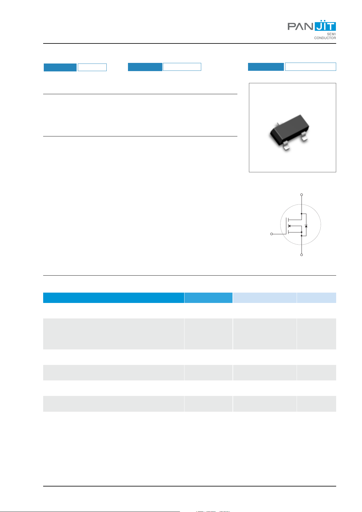
P ACKAGE SOT-23
D
G
ABSOLUTE MAXIMUM RATIN GS
TA = 25OC Unless otherwise noted.
retemaraP lobmyS
egatloVecruoS-niarDV
M1sgR(egatloVetaG-niarD Ω) VDRG 06 V
≤
suounitnoC-egatloVecruoSetaG
desluP-
05<pt(evititepeRoN- µ )s
suounitnoC-tnerruCniarDmumixaM
52evobAdetareDnoitapissiDrewOPmumixaM
egnaRerutarepmeTegarotSdnanoitarepOT
tneibmA-ot-noitcnuJ,ecnatsiseRlamrehT RθJA 526
S
2007N2 stinU
DSS 06V
02
V GSS
D
I
O
C P D 002 Wm
J ,TSTG 051+ot55-/Wm
±
02
±
511
008
V
Am
O
C
O
W/C
Part Number: 2N7002 PAGE 1
Page 2
ELECTRICAL CHARACTERISTICS
TA = 25OC Unless otherwise noted.
retemaraP lobmyS snoitidnoC
SCITSIRETCARAHCFFO
egatloVnwodkaerBecruoS-niarDVB
tnerruCniarDegatloVetaGoreZ I
drawroF,egakaeLydoB-etaGI
esreveR,egakaeLydoB-etaG I
SCITSIRETCARAHCNO
)1eton(
egatloVdlohserhTetaG V
ecnatsiseR-nOecruoS-niarDcitatSR
egatloV-nOecruoS-niarD VDS(ON)
tnerruCniarDetatS-nOI
ecnatcudnocsnarTdrawroF G
DSS
DSS
GSSF
GSSR
GS
)ht( V
DS(ON
)VGS,V01=ID005=mA,TJ001=OC- 2.15.7
D(ON)
FS
V
V
DS
V
DS
V
DS
V
DS
DSV=GS,ID
V
GS
V
GS
V
GS
V
DSV2DS(ON
≥
GS
,V0=ID01= µA06-- V
,V06=VGSV0=,TJ52=OC
,V06=VGSV0=,TJ521=OC
,V0=VGSV02=--001An
,V0=VGS=V02- - - 001- An
052= µA 1 1.2 5.2 V
,V01=ID005=mA
,V0.5=ID05=mA
,V01=VDSV2DS(ON)0050072- Am
≥
,)ID002=mA 08 023 - Sm
.niM .pyT .xaM stinU
-
-
-
-
-
-
06.0
90.0
0.1
5.0
57.3
05.1
µA
Am
Ω
V
SCITSIRETCARAHCCIMANYD
ecnaticapaCtupnI C
ecnaticapaCtuptuO C
ecnaticapaCrefsnarTesreveR C
emiTnO-nruT T
emiTffO-nruT T
Note:
1.Pulse Test: Pulse Width ≤ 300µs, Duty Cycle ≤ 2.0%
ISS
OSS
RSS
ON
OFF
V
V
V
DS
,V52=VGS,V0=zHM0.1=F - 02 05 Fp
V
DS
,V52=VGS,V0=zHM0.1=F - 11 52 Fp
V
DS
,V52=VGS,V0=zHM0.1=F - 4 5 Fp
DD
DD
,V03=RL051= Ω,I
V
GS
,V03=RL051= Ω,I
V
GS
,V01=R
GEN
,V01=R
GEN
D
D
52= Ω
52= Ω
Am002=
Am002=
- - 02 sn
- - 02 sn
Part Number: 2N7002 PAGE 2
Page 3

RATING and CHARACTERISTIC CURVES
2.0
1.5
V =10V
GS
9.0
8.0
7.0
6.0
1.0
5.0
4.0
3.0
D
I , Drain-Source Current (A)
0.5
0
012345
V , Drain-Source Coltage (V)
DS
On-Region Characteristics
V =10V I
GS D
2.0
1.5
=500mA
3.0
V =4.0V
GS
2.5
2.0
4.5
6.0 7.05.0
8.0
1.5
1.0
0.5
)
0 0.4 0.8 1.2 1.6 2.0
ON
(
DS
R , Normalized Drain-Source On-Resistance
I , Drain Current (A)
D
On-Resistance v.s. Gate Voltage and Drain Current
V =10V
GS
3.0
2.5
2.0
T = 125 C
J
O
9.0
10
1.0
0.5
)
-50 -25 0 25 50 75 100 125 150
ON
(
DS
R , Normalized Drain-Source On-Resistance
T , Junction Temperature ( C)
J
O
On-Resistance v.s Temperature
DS
V =10V
D
I , Drain Current (A)
2.0
1.6
1.2
0.8
0.4
T = -55 C
J
O
25 C
1.5
O
25 C
1.0
-55 C
O
0.5
)
0
ON
0 0.4 0.8 1.2 1.6 2.0
(
DS
R , Normalized Drain-Source On-Resistance
I , Drain Current (A)
D
On-Resistance v.s Drain
V= I
DS D
GS
1.1
O
O
125 C
1.0
0.9
= 1mAV
0
0246810
V , Gate to Source Voltage (V)
GS
Transfer Characteristics
0.8
-50 -25 0 25 50 75 100 125 150
th
V , Normalized Gate-Source Threshold Voltage (V)
T , Junction Temperature ( C)
J
O
Gate Threshold v.s. Temperature
Part Number: 2N7002 PAGE 3
Page 4

RATING and CHARACTERISTIC CURVES
ID=250 Am
1.10
1.05
1.00
Breakdown Voltage (V)
DSS
0.95
BV , Normalized Drain-Source
0.925
-50 -25 0 25 50 75 100 125 150
T , Junction Temperature ( C)
J
Breakdown Voltage v.s. Temperature
f=1MHz V =0V
50
20
10
5
GS
Capactance (pF)
2
1
1 2 3 5 10 20 30 50
V=0V
GS
1
O
T = 125 C
0.1
0.01
J
O
25 C
-55 C
O
Is, Reverse Drain Current (A)
0.001
0.2 0.4 0.6 0.8 1.0 1.2 1.4
O
V , Body Diode Forward Voltage (V)
SD
Body Diode Forward Voltage v.s. Current and Temperature
V 25V
DS =
10
C
ISS
C
oss
C
rss
8
6
ID = 500mA
4
2
GS
V , Gate to Source Voltage (V)
0
0 0.1 0.8 1.2 1.6 2.0
280mA
115mA
r(t) , Normailized Effective
Transient Thermal Resistance
V , Drain to Source Voltage (V)
DS
Capacitance Characteristics
1
0.5
0.2
0.1
0.05
0.01
0.02
0.001
0.0001 0.001 0.01 0.1
Transient Thermal Respone Curve
,Time (sec)
Tt
Q , Gate Charge (nC)
g
Gate Charge Characteristics
RJA
q
(t) (t)
=r R JA*q
R JA = (See Datasheet)
q
P
(pk)
t
1
T-T=P RJA
JA
Duty Cycle, D =
1
10 100
t
2
*q
(t)
t/t
12
300
Part Number: 2N7002 PAGE 4
Page 5

RATING and CHARACTERISTIC CURVES
100ms
A=
10ms
O
1m
s
V =10V, Single Pulse T 25 CGS
3
2
1
D
I , Drain Current (A)
0.5
0.1
0.05
0.01
0.005
DS(ON)
R Limit
DC
12 5 1020306080
V , Drain-Source Voltage (V)
DS
10s
1s
Maximum Safe Operating Area
100 sm
t
d(on)
V
DD
R
L
V
V
IN
V
GS
R
GEN
G
D
OUT
DUT
S
Switching Test Circuit
t
on
t
r
t
90% 90%
d(off)
t
off
t
f
V
V
OUT
IN
10%
10%
50% 50%
Pulse Width
Switching Waveforms
90%
10%
Inverted
Part Number: 2N7002 PAGE 5
Page 6

OUTLINE DRAWING
.119(3.00
.110(2.80
)
)
SOT-23
MIN.
)
.20
(
.007
MAX.
)
.15
(
.006
.083(2.10
.066(1.70
.020(.50
.013(.35
)
)
1.20
1.40
(
(
.047
.056
)
)
.90
(
.035
.006(.15
.002(.05
)
)
)
)
1.10
(
.044
)
)
)
2.60
(
.103
)
2.20
(
.086
Part Number: 2N7002 PAGE 6
 Loading...