

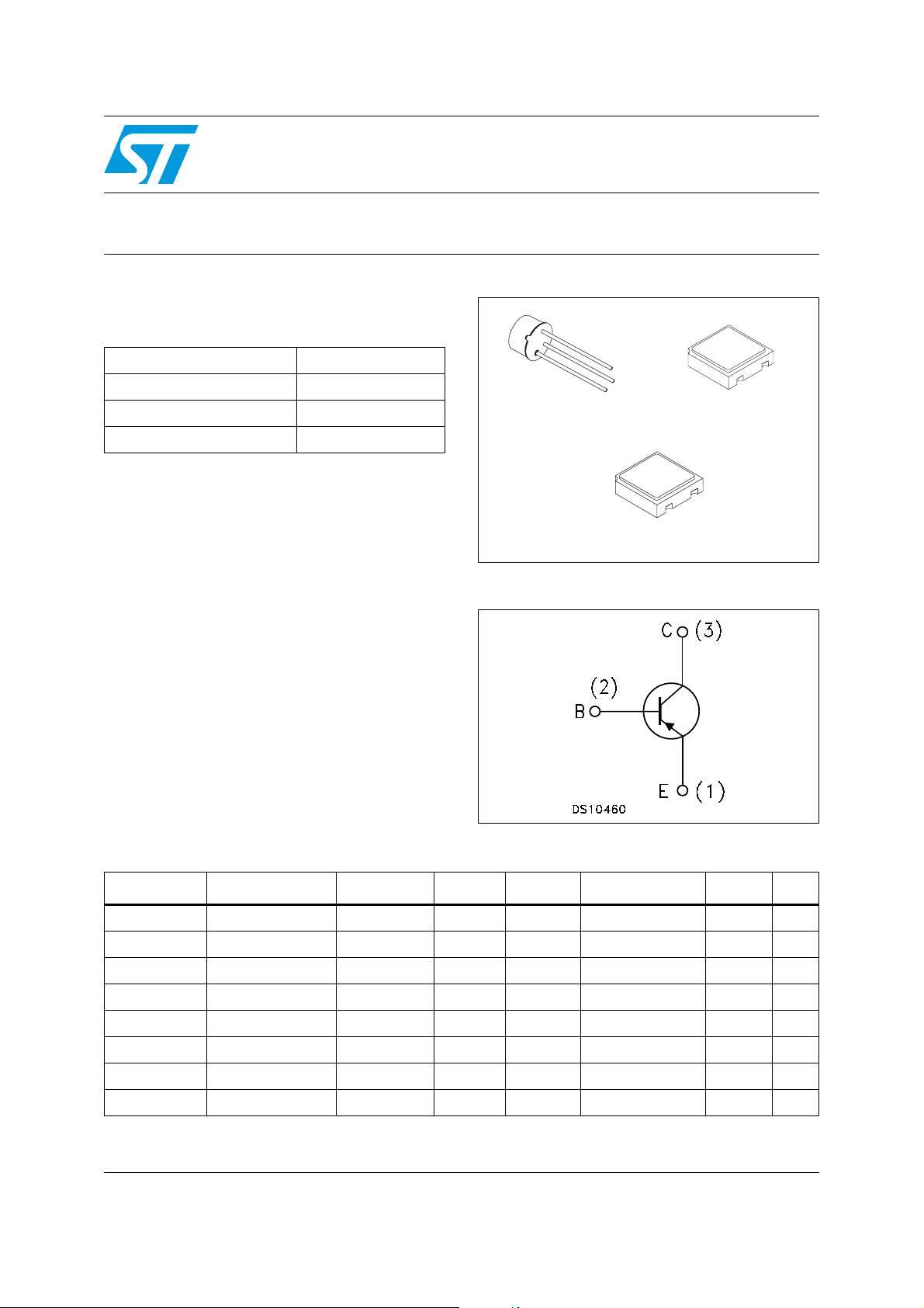
Hi-Rel PNP bipolar transistor 150 V - 0.5 A
Features
BV
CEO
IC (max) 0.5 A
H
at 10 V - 150 mA > 60
FE
Operating temperature range -65°C to +200°C
150 V
2N5401HR
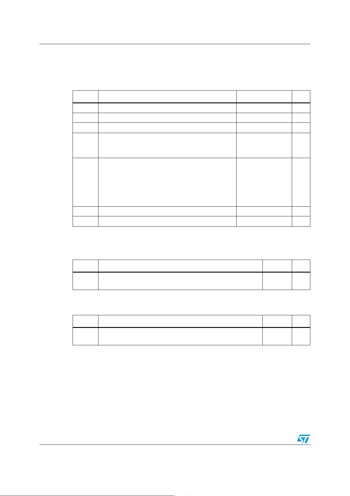
3
1
2
3
TO-18 LCC-3
3
1
2
■ Hi-Rel PNP bipolar transistor
■ Linear gain characteristics
■ ESCC qualified
■ European preferred part list - EPPL
■ 100 krad low dose rate
■ Radiation level: lot specific total dose contact
Figure 1. Internal schematic diagram
4
1
2
LCC-3UB
marketing for specified level
Description
The 2N5401HR is a silicon planar epitaxial PNP
transistor in TO-18 and LCC-3 packages. It is
specifically designed for aerospace Hi-Rel
applications and ESCC qualified according to the
5202-014 specification. In case of conflict
between this datasheet and ESCC detailed
specification, the latter prevails.
Table 1. Device summary
Order codes ESCC Part num. Quality Level Rad level Packages Lead Finish Mass (g) EPPL
2N5401UB1 - Eng. Model LCC-3UB Gold 0.06 -
SOC5401SW 5202/014/07 ESCC Flight 100 krad LCC-3 Solder Dip 0.06 Y
2N5401UB06 5202/014/06 ESCC Flight LCC-3UB Gold 0.06 -
2N5401UB07 5202/014/07 ESCC Flight LCC-3UB Solder Dip 0.06 -
SOC5401 - Eng. Model LCC-3 Gold 0.06 -
SOC5401HRB 5202/014/04 or 05 ESCC Flight LCC-3 Gold/Solder Dip
(1)
0.06 Y
2N5401/T1 - Eng. Model TO-18 Gold 0.40 -
2N5401HR 5202/014/01 or 02 ESCC Flight TO-18 Gold/Solder Dip
1. Depending ESCC part number mentioned on the purchase order.
(1)
0.40 -
July 2010 Doc ID 16934 Rev 2 1/10
www.st.com
10
Electrical ratings 2N5401HR
1 Electrical ratings
Table 2. Absolute maximum ratings
Symbol Parameter Value Unit
V
V
V
Collector-base voltage (IE = 0) -160 V
CBO
Collector-emitter voltage (IB = 0) -150 V
CEO
Emitter-base voltage (IC = 0) -5 V
EBO
Collector current
I
for 2N5401HR
C
for SOC5401HRB
Total dissipation at T
amb
≤ 25 °C
for 2N5401HR
P
for SOC5401HRB
TOT
for SOC5401HRB
(1)
-0.6
-0.5
0.36
0.36
0.58
Total dissipation at Tc ≤ 25 °C
for 2N5401HR
T
1. When mounted on a 8x10x0.6 mm ceramic substrate.
Storage temperature -65 to 200 °C
STG
T
Max. operating junction temperature 200 °C
J
1.2
Table 3. Thermal data for through-hole package
Symbol Parameter Value Unit
R
R
Thermal resistance junction-case __ max
thJC
Thermal resistance junction-ambient __ max
thJA
146
486
°C/W
°C/W
A
A
W
W
W
W
Table 4. Thermal data for SMD package
Symbol Parameter Value Unit
R
1. When mounted on a 8x10x0.6 mm ceramic substrate.
2/10 Doc ID 16934 Rev 2
Thermal resistance junction-ambient __ max
thJA
Thermal resistance junction-ambient
(1)
__ max
486
302
°C/W
°C/W
2N5401HR Electrical characteristics
2 Electrical characteristics
T
= 25 °C unless otherwise specified.
case
Table 5. Electrical characteristics
Symbol Parameter Test conditions Min. Typ. Max. Unit
I
CBO
I
EBO
V
(BR)CBO
V
(BR)CEO
V
(BR)EBO
V
CE(sat)
V
BE(sat)
h
FE
Collector-base cut-off
current (I
= 0)
E
Emitter-base cut-off
current (I
= 0)
C
= -120 V
V
CB
V
= -120 V TC = 150 °C
CB
= -3 V -50 nA
V
EB
-50
-50nAµA
Collector-base
breakdown voltage
= 0)
(I
E
= -100 µA -160 V
I
C
Collector-emitter
(1)
breakdown voltage
(I
= 0)
B
= -1 mA -150 V
I
C
Emitter-base
breakdown voltage
= 0)
(I
C
Collector-emitter
(1)
saturation voltage
Base-emitter
(1)
saturation voltage
(1)
DC current gain
h
fe
Small signal current
gain
= -10 µA -5 V
I
E
= -10 mA IB = -1 mA
I
C
IC = -50 mA IB = -5 mA
= -10 mA IB = -1 mA
I
C
IC = -50 mA IB = -5 mA
= -1 mA V
I
C
IC = -10 mA V
I
= -50 mA V
C
IC = -10 mA V
T
= -55 °C
amb
= -10 V IC = -10 mA
V
CE
CE
CE
CE
CE
= -5 V
= -5 V
= -5 V
= -5 V
f = 10 kHz
50
60
60
20
5
-0.2
-0.5
-1
-1
240
V
V
V
V
C
obo
1. Pulsed duration = 300 µs, duty cycle ≤ 2 %
Output capacitance
(I
= 0)
E
V
Doc ID 16934 Rev 2 3/10
= -10 V f = 1 MHz 6 pF
CB

Package mechanical data 2N5401HR
3 Package mechanical data
In order to meet environmental requirements, ST offers these devices in different grades of
ECOPACK
specifications, grade definitions and product status are available at:
ECOPACK
®
packages, depending on their level of environmental compliance. ECOPACK®
®
is an ST trademark.
www.st.com
.
4/10 Doc ID 16934 Rev 2
2N5401HR Package mechanical data
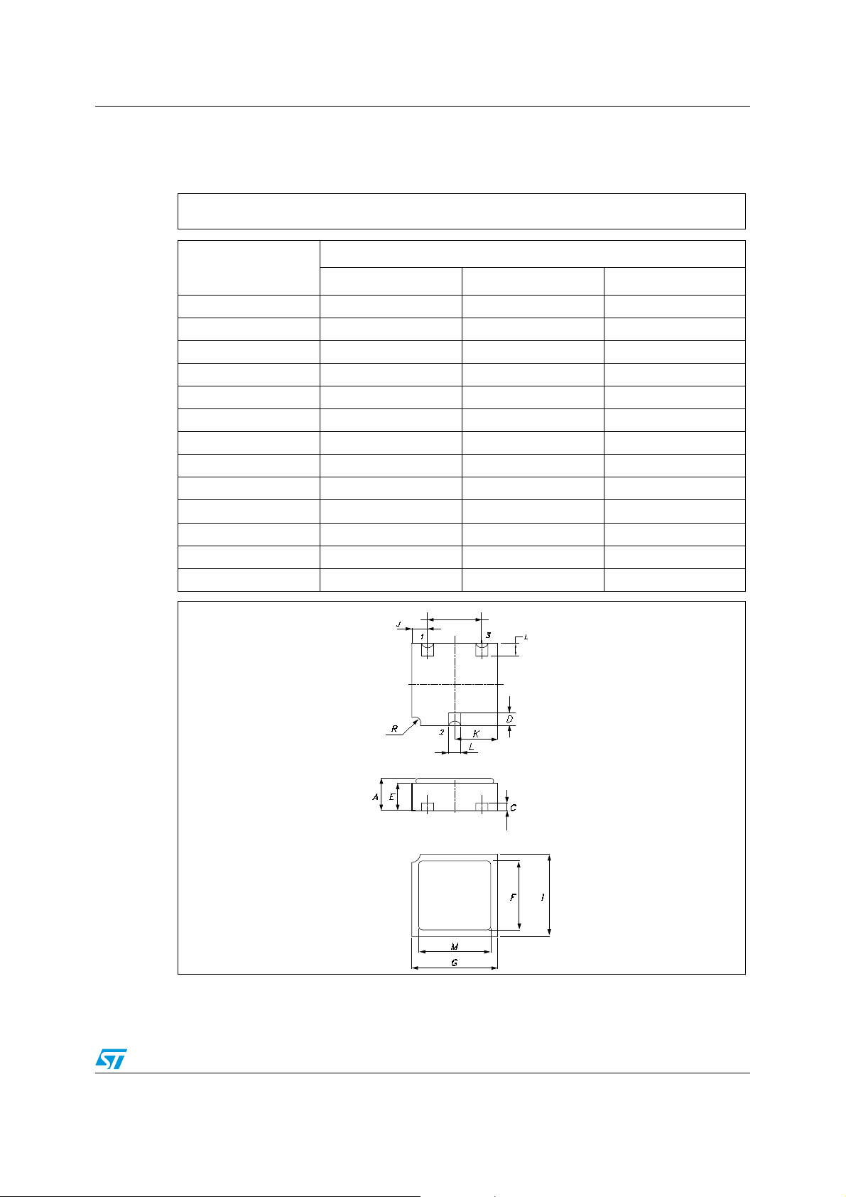
LCC-3 mechanical data
Dim.
Min. Typ. Max.
A 1.16 1.42
C 0.45 0.50 0.56
D0.600.760.91
E0.911.011.12
F1.952.03 2.11
G2.92 3.05 3.17
I 2.41 2.54 2.66
J 0.42 0.57 0.72
K1.371.521.67
L 0.40 0.50 0.60
M 2.46 2.54 2.62
N1.801.902.00
R0.30
N
mm.
0041211
Doc ID 16934 Rev 2 5/10

Package mechanical data 2N5401HR
LCC-3UB mechanical data
Dim.
A1.16 1.42
C 0.46 0.51 0.56
D 0.56 0.76 0.96
E0.92 1.02 1.12
F1.952.03 2.11
G2.92 3.05 3.18
I 2.41 2.54 2.67
J 0.42 0.57 0.72
K1.37 1.52 1.67
L 0.41 0.51 0.61
M 2.46 2.54 2.62
N1.811.91 2.01
r0.20
r1 0.30
r2 0.56
Min. Typ. Max.
mm.
6/10 Doc ID 16934 Rev 2
8206487

2N5401HR Package mechanical data
D
Doc ID 16934 Rev 2 7/10

Order codes 2N5401HR
4 Order codes
Table 6. Order codes
Order codes
2N5401UB1 - LCC-3UB Gold 2N5401UB1 - Waffle pack
SOC5401SW 5202/014/07 100 krad LCC-3 Solder Dip 520201407 Y Waffle pack
2N5401UB06 5202/014/06 LCC-3UB Gold 520201406 - Waffle pack
2N5401UB07 5202/014/07 LCC-3UB Solder Dip 520201407 - Waffle pack
SOC5401 - LCC-3 Gold SOC5401 - Waffle pack
SOC5401HRB
2N5401/T1 - TO-18 Gold 2N5401/T1 - Strip pack
2N5401HR
1. Depending ESCC part number mentioned on the purchase order.
ESCC Part
number
5202/014/04
or 05
5202/014/01
or 02
Radiation
level
Packages Lead Finish Marking EPPL Packing
(1)
LCC-3 Gold/Solder Dip
TO-18 Gold/Solder Dip
520201404 or 05 Y Waffle pack
(1)
520201401 or 02 - Strip pack
Contact ST sales office for information about the specific conditions for:
– Products in die form
– Tape and reel packing
8/10 Doc ID 16934 Rev 2

2N5401HR Revision history
5 Revision history
Table 7. Document revision history
Date Revision Changes
04-Jan-2010 1 Initial release
26-Jul-2010 2 Modified
Table 1 on page 1
, added
Table 6 on page 8
Doc ID 16934 Rev 2 9/10

2N5401HR
Please Read Carefully:
Information in this document is provided solely in connection with ST products. STMicroelectronics NV and its subsidiaries (“ST”) reserve the
right to make changes, corrections, modifications or improvements, to this document, and the products and services described herein at any
time, without notice.
All ST products are sold pursuant to ST’s terms and conditions of sale.
Purchasers are solely responsible for the choice, selection and use of the ST products and services described herein, and ST assumes no
liability whatsoever relating to the choice, selection or use of the ST products and services described herein.
No license, express or implied, by estoppel or otherwise, to any intellectual property rights is granted under this document. If any part of this
document refers to any third party products or services it shall not be deemed a license grant by ST for the use of such third party products
or services, or any intellectual property contained therein or considered as a warranty covering the use in any manner whatsoever of such
third party products or services or any intellectual property contained therein.
UNLESS OTHERWISE SET FORTH IN ST’S TERMS AND CONDITIONS OF SALE ST DISCLAIMS ANY EXPRESS OR IMPLIED
WARRANTY WITH RESPECT TO THE USE AND/OR SALE OF ST PRODUCTS INCLUDING WITHOUT LIMITATION IMPLIED
WARRANTIES OF MERCHANTABILITY, FITNESS FOR A PARTICULAR PURPOSE (AND THEIR EQUIVALENTS UNDER THE LAWS
OF ANY JURISDICTION), OR INFRINGEMENT OF ANY PATENT, COPYRIGHT OR OTHER INTELLECTUAL PROPERTY RIGHT.
UNLESS EXPRESSLY APPROVED IN WRITING BY AN AUTHORIZED ST REPRESENTATIVE, ST PRODUCTS ARE NOT
RECOMMENDED, AUTHORIZED OR WARRANTED FOR USE IN MILITARY, AIR CRAFT, SPACE, LIFE SAVING, OR LIFE SUSTAINING
APPLICATIONS, NOR IN PRODUCTS OR SYSTEMS WHERE FAILURE OR MALFUNCTION MAY RESULT IN PERSONAL INJURY,
DEATH, OR SEVERE PROPERTY OR ENVIRONMENTAL DAMAGE. ST PRODUCTS WHICH ARE NOT SPECIFIED AS "AUTOMOTIVE
GRADE" MAY ONLY BE USED IN AUTOMOTIVE APPLICATIONS AT USER’S OWN RISK.
Resale of ST products with provisions different from the statements and/or technical features set forth in this document shall immediately void
any warranty granted by ST for the ST product or service described herein and shall not create or extend in any manner whatsoever, any
liability of ST.
ST and the ST logo are trademarks or registered trademarks of ST in various countries.
Information in this document supersedes and replaces all information previously supplied.
The ST logo is a registered trademark of STMicroelectronics. All other names are the property of their respective owners.
© 2010 STMicroelectronics - All rights reserved
STMicroelectronics group of companies
Australia - Belgium - Brazil - Canada - China - Czech Republic - Finland - France - Germany - Hong Kong - India - Israel - Italy - Japan -
Malaysia - Malta - Morocco - Philippines - Singapore - Spain - Sweden - Switzerland - United Kingdom - United States of America
www.st.com
10/10 Doc ID 16934 Rev 2
 Loading...