

Page 1
C
B
E
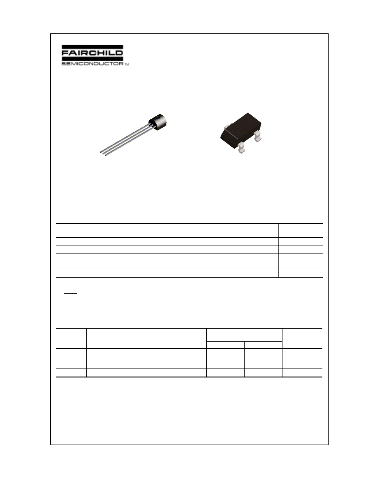
TO-92
PNP General Purpose Amplifier
This device is designed as a general purpose amplifier and switch
for applications requiring high voltages. Sourced from Process 74.
MMBT54012N5401
C
SOT-23
Mark: 2L
2N5401 / MMBT5401
Discrete POWER & Signal
Technologies
E
B
Absolute Maximum Ratings* TA = 25°C unless otherwise noted
Symbol Parameter Value Units
V
CEO
V
CBO
V
EBO
I
C
TJ, T
stg
Collector-Emitter Voltage 150 V
Collector-Base Voltage 160 V
Em i t ter - Bas e V olt ag e 5. 0 V
Collector Current - Continuous 200 mA
Operating and Storage Junction Temperature Range -55 to +150
°C
*These ratings are limiting values above which the serviceability of any semiconductor device may be impaired.
NOTES:
1) These ratings are based on a maximum junction temperature of 150 degrees C.
2) These are steady state limits. The factory should be consulted on applications involving pulsed or low duty cycle operations.
Thermal Characteristics TA = 25°C unless otherwise noted
Symbol Characteristic Max Units
2N5401 *MMBT5401
P
D
R
θ
JC
R
θ
JA
*Device mounted on FR-4 PCB 1.6" X 1.6" X 0.06."
Total De vice Dissip at i on
Derate above 25°C
Thermal Resistance, Junction to Case 83.3 °C/W
Thermal Resistance, Junction to Ambient 200 357
625
5.0
350
2.8
mW
mW/°C
°C/W
1997 Fairchild Semiconductor Corporation
Page 2

PNP General Purpose Amplifier
(continued)
Electrical Characteristics TA = 25°C unless otherwise noted
Symbol Parameter Test Conditions Min Max Units
OFF CHARACTERISTICS
V
(BR)CEO
V
(BR)CBO
V
(BR)EBO
I
CBO
I
EBO
ON CHARACTERISTICS*
h
FE
V
sat
CE(
V
sat
BE(
Collector-Emitter Breakdown Voltage* IC = 1.0 m A, IB = 0 150 V
C oll ec t or -Base Breakd ow n Volt age IC = 100 µA, IE = 0 160 V
Em i t ter - Bas e B r e akdown Vol tage
= 10 µA, IC = 0
I
E
Colle c tor Cu tof f Cu r ren t VCB = 120 V, I
VCB = 120 V, I
E
E
= 0
= 0, T
= 100°C
A
5.0 V
Emit ter Cutoff C u rre nt VEB = 3.0 V, IC = 0 50 nA
DC Cu r re n t Ga in IC = 1.0 m A, VCE = 5.0 V
I
= 10 mA, VCE = 5.0 V
C
= 50 mA, VCE = 5.0 V
I
Collector-Emitter Saturation Voltage IC = 10 mA, IB = 1.0 mA
)
Base-Emitter Saturation Voltage IC = 10 mA, IB = 1.0 mA
)
C
= 50 mA, IB = 5.0 mA
I
C
= 50 mA, IB = 5.0 mA
I
C
50
60
50
50
50
240
0.2
0.5
1.0
1.0
nA
µ
A
V
V
V
V
2N5401 / MMBT5401
SMALL SIGNAL CHARACTERISTICS
f
T
C
obo
NF Noise Figure
Current Gain - Bandwidth Product IC = 10 mA, VCE = 10 V,
f = 10 0 M Hz
Output Capacitance VCB = 10 V, IE = 0,
f = 1. 0 MHz
= 250 µA, VCE = 5.0 V,
I
C
= 1.0 kΩ,
R
S
f = 10 Hz to 15.7 kHz
100 300 MHz
6.0 pF
8.0 dB
*Pulse Test: Pulse Width ≤ 300 µs, Duty Cycle ≤ 2.0%
Spice Model
PNP (Is=21.48f Xti=3 Eg=1.11 Vaf=100 Bf=132.1 Ne=1.375 Ise=21.48f Ikf=.1848 Xtb=1.5 Br=3.661 Nc=2
Isc=0 Ikr=0 Rc=1.6 Cjc=17.63p Mjc=.5312 Vjc=.75 Fc=.5 Cje=73.39p Mje=.3777 Vje=.75 Tr=1.476n Tf=641.9p
Itf=0 Vtf=0 Xtf=0 Rb=10)
Page 3

Typical Characteristics
2N5401 / MMBT5401
PNP General Purpose Amplifier
(continued)
Typical Pulsed Current Gain
vs Collector Current
200
V = 5V
CE
150
100
- 40 ºC
50
0
0.0001 0.001 0.01 0.1 1
FE
h - TYPICAL PULSED CURRENT GAIN
125 °C
25 °C
I - COLLECTOR CURRENT (A)
C
Base-Emitter Saturation
Voltage vs Collector Current
1
0.8
0.6
0.4
0.2
BESAT
V - BASE-EMITTER VOLTAGE (V)
0.1110100
- 40 ºC
25 °C
125 ºC
ββ
I - COLLECTOR CURRENT (mA)
C
= 10
Coll ecto r-Emitte r Satu rati on
Vo ltage vs Col lector Cur rent
0.4
ββ
= 10
0.3
0.2
0.1
0
0.1 1 10 100
CESAT
V - COLLECTOR-EMITTER VOLTAGE (V)
I - COLLECTOR CURRENT (mA)
C
125 ºC
25 °C
- 40 ºC
Base-Emitter ON Voltage vs
Collector Current
1
0.8
0.6
0.4
0.2
0.1 1 10 100
BE(ON)
V - BASE-EMITTER ON VOLTAGE (V)
- 40 ºC
25 °C
125 ºC
V = 5V
CE
I - COLLE CT O R CURRENT (mA)
C
Collector-Cutoff Current
vs Ambient Temperature
100
V = 100V
CB
10
1
0.1
CBO
I - COLLECTOR CURRENT (nA)
25 50 75 100 125 150
T - AMBIENT TEMPERATURE ( C)
A
º
Collector-Emitter Breakdown
Voltage with Resistance
Between Emitter-Base
220
210
200
190
180
170
CER
0.1 1 10 100 1000
BV - BREAKDOWN VOLTAGE (V)
RESISTANCE (k )
ΩΩ
Page 4

Typical Characteristics (continued)
2N5401 / MMBT5401
PNP General Purpose Amplifier
(continued)
Input and Output Capacitance
vs Reverse Voltage
80
60
40
20
CAPACITANCE (pF)
0
0.1 1 10 100
V - REVERSE BIAS VOLTAGE(V)
R
C
f = 1.0 MHz
eb
C
Power Dissipation vs
Ambient Temperature
700
600
500
SOT -23
400
300
200
cb
100
D
P - POWER DI SSIPATION (mW)
0
0 25 50 75 100 125 150
TO-92
TEMPERATURE ( C)
o
 Loading...