

Page 1

PIC12(L)F1612/16(L)F1613
8/14/16-Pin, 8-Bit Flash Microcontroller
Description:
PIC12(L)F1612/16(L)F1613 microcontrollers deliver
on-chip features that are unique to the design for
embedded control of small motors and general purpose
applications in 8 and 14-pin count packages. Features
like 10-bit A/D, CCP, 24-bit SMT and Zero-Cross
Detection offer an excellent solution to a variety of
applications. The CRC and Window WDT are provided
to support safety-critical applications in home
appliances and white goods.
Core Features:
• C Compiler Optimized RISC Architecture
• Only 49 Instructions
• Operating Speed:
- 0-32 MHz clock input
- 125 ns minimum instruction cycle
• Interrupt Capability with Automatic Context
Saving
• 16-Level Deep Hardware Stack with Optional
Overflow/Underflow Reset
• Direct, Indirect and Relative Addressing modes:
- Two full 16-bit File Select Registers (FSRs)
- FSRs can read program and data memory
• Power-on Reset (POR)
• Power-up Timer (PWRT)
• Brown-out Reset (BOR) with Selectable Trip Point
• Windowed Watchdog Timer (WWDT):
- Variable prescaler selection
- Variable window size selection
- All sources configurable in hardware or
software
Memory:
• Up to 2 Kwords Flash Program Memory
• Up to 256 Bytes Data SRAM Memory
• Direct, Indirect and Relative Addressing modes
Operating Characteristics:
• In-Circuit Serial Programming™ (ICSP™) via Two
Pins
• Enhanced Low-Voltage Programming (LVP)
• Operating Voltage Range:
- 1.8V to 3.6V (PIC12LF1612/16LF1613)
- 2.3V to 5.5V (PIC12F1612/16F1613)
• Programmable Code Protection
• Self-Programmable under Software Control
Clocking Structure:
• Precision Internal Oscillator:
- Factory calibrated to ±1%, typical
- Software-selectable frequency range from
32 MHz to 31 kHz
• 31 kHz Low-Power Internal Oscillator
• External Oscillator Block with:
- Three external clock modes up to 32 MHz
• 4x Phase-Locked Loop (PLL)
Digital Peripherals:
• Up to 11 I/O Pins and one Input-only Pin:
- Individually programmable interrupt-onchange pins
- Individually programmable weak pull-ups
- Individual programmable digital port controls
(Input level selection, open drain, slew rate
control)
• Timer0: 8-Bit Timer/Counter with 8-Bit
Programmable Prescaler
• Enhanced Timer1:
- 16-bit timer/counter with prescaler
- External Gate Input mode
- Timer Clock In (T1CKI)
• Enhanced Timer2/4/6:
- 8-bit timer/counter with 8-bit period register
- 1:1 up to 1:16 linear Postscaler
- 1:1 up to 128:1 Prescaler
- Asynchronous clock source capability
- External Reset/Gate sources
- One-shot count operation
• Two Capture, Compare, PWM modules:
- 16-bit Capture/Compare
-10-bit PWM
• Two Signal Measurement Timers (SMT):
- 24-bit Signal Measurement Timer
- Up to 12 different Acquisition modes
- Two 24-bit result Buffer registers
- Input polarity control
• 16-Bit CRC:
- Software-selectable polynomial
- Software-selectable data width
- Integrated CCPR memory scan capability for
memory integrity checking
2014 Microchip Technology Inc. Preliminary DS40001737A-page 1
Page 2

PIC12(L)F1612/16(L)F1613
Digital Peripherals (Continued):
• Complementary Waveform Generator (CWG):
- Multiple signal sources
- True and complement from any source
- Programmable one to four crossover
- Programmable dead band
- Fault-shutdown input
Analog Peripherals:
• Analog-to-Digital Converter (ADC):
- 10-bit resolution
- Up to eight channels
• Voltage Reference module:
- Fixed Voltage Reference (FVR) with 1.024V,
2.048V and 4.096V output levels
- 8-bit rail-to-rail resistive DAC with positive
reference selection
• Zero Cross Detector:
- Detect when AC signal on pin passes through
ground
• Up to Two Comparators:
- Rail-to-rail inputs
- Power mode control
- Software-controllable hysteresis
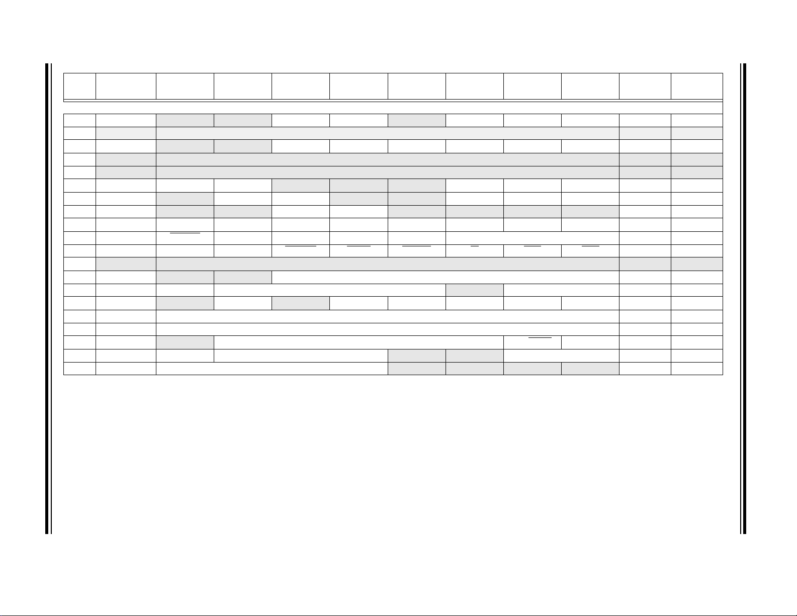
TABLE 1: PIC12/16(L)F161X FAMILY TYPES
Packages:
• PIC12(L)F1612:
- 8-pin: PDIP, SOIC, DFN
• PIC16(L)F1613:
- 14-pin: PDIP, SOIC, TSSOP
- 16-pin: QFN (4x4x0.9)
Debug Features:
• In-Circuit Debug (ICD):
- Integrated: supports all services
- Header: not required
•Emulation:
- Header: supports all devices
Device
Data Sheet Index
PIC12(L)F1612 (A) 2048 256 6 1/1 1 4 1 2/0 1 0 2/3 0 Y Y 0 0 0 I/H
PIC16(L)F1613 (A) 2048 256 12 1/1 2 8 1 2/0 1 0 2/3 0 Y Y 0 0 0 I/H
PIC16(L)F1614 (B) 4096 512 12 1/3 2 8 1 2/2 1 2 2/3 1 Y Y 1 1 1 I/H
PIC16(L)F1615 (C) 8192 1024 12 1/3 2 8 1 2/2 1 4 2/3 1 Y Y 1 1 1 I/H
PIC16(L)F1618 (B) 4096 512 18 1/3 2 12 1 2/2 1 2 2/3 1 Y Y 1 1 1 I/H
PIC16(L)F1619 (C) 8192 1024 18 1/3 2 12 1 2/2 1 4 2/3 1 Y Y 1 1 1 I/H
Note 1: Debugging Methods: (I) – Integrated on Chip; (H) – via ICD Header; E – using Emulation Product.
Data Sheet Index:
A. DS40001737 PIC12(L)F1612/16(L)F1613 Data Sheet, 8/14-Pin, 8-bit Flash Microcontrollers
B. Future Release PIC16(L)F1614/8 Data Sheet, 14/20-Pin, 8-bit Flash Microcontrollers
C. Future Release PIC16(L)F1615/9 Data Sheet, 14/20-Pin, 8-bit Flash Microcontrollers
(W)
(bytes)
Data SRAM
Program Memory Flash
I/O Pins
Comparators
8-bit/16-bit Timers
10-bit ADC (ch)
Zero-Cross Detect
CCP/10-bit PWM
CLC
CWG
SMT/HLT
Timer
Angular Timer
Window Watchdog
Math Accelerator
CRC with Memory Scan
EUSART
C™/SPI
2
I
Note: For other small form-factor package availability and marking information, please visit
http://www.microchip.com/packaging or contact your local sales office.
(1)
Debug
DS40001737A-page 2 Preliminary 2014 Microchip Technology Inc.
Page 3
PIC12(L)F1612/16(L)F1613
1
2
3
4
8
7
6
5
VDD
RA5
RA3
V
SS
RA0
RA1
RA2
Note: See Table 2 for location of all peripheral functions.
RA4
PIC12F1612
PIC12LF1612
PIC16F1613
1
2
3
4
14
13
12
11
5
6
7
10
9
8
VDD
RA5
RA4
RA3
RC5
RC4
V
SS
RA0
RA1
RA2
RC0
RC1
RC2
RC3
Note: See Table 3 for location of all peripheral functions.
PIC16LF1613
PIC16F1613
PIC16LF1613
RA0
RA1
RA2
RC0
9
10
11
12
5
6
RC4
RC3
RC1
RC2
7
8
2
3
1
4
RA5
RA4
RA3/
MCLR/VPP
RC5
15
16
13
14
NC
VDD
NC
VSS
Note 1: See Ta bl e 3 for location of all peripheral functions.
2: For the QFN package, it is recommended that the bottom pad be connected to V
SS.
PIN DIAGRAMS
Pin Diagram – 8-PIN PDIP, SOIC, DFN, UDFN
Pin Diagram – 14-PIN PDIP, SOIC, TSSOP
Pin Diagram –
2014 Microchip Technology Inc. Preliminary DS40001737A-page 3
16-PIN QFN
Page 4
PIC12(L)F1612/16(L)F1613
PIN ALLOCATION TABLE
TABLE 2: 8-PIN ALLOCATION TABLE FOR PIC12(L)F1612
I/O
RA0 7 AN0 DAC1OUT1 C1IN+ — CCP2 CWG1B — IOC — Y ICSPDAT
RA1 6 AN1 VREF+ C1IN0- — — — ZCD1OUT IOC — Y ICSPCLK
RA2 5 AN2 — C1OUT T0CKI
RA3 4 — — — T1G
RA4 3 AN3 — C1IN1- T1G — CWG1B — IOC SMTSIG1 Y CLKOUT
RA5 2 — — — T1CKI
VDD 1 — — — — — — — — — — VDD
Vss 8 — — — — — — — — — — VSS
Note 1: Alternate pin function selected with the APFCON register (Register 12-1).
A/D
Reference
8-Pin PDIP/SOIC/DFN
Comparator
Timers
T4IN
(1)
T6IN
T2IN
CCP
(1)
CCP1
— —
CCP1 CWG1A — IOC SMTWIN1 Y CLKIN
CWG1A
CWG1IN
CWG
(1)
ZCD
ZCD1IN INT
—
IOC
IOC SMTWIN2 Y
Interrupt
SMT
SMTSIG2 Y —
Pull-up
MCLR
VPP
TABLE 3: 14-PIN AND 16-PIN ALLOCATION TABLE FOR PIC16(L)F1613
I/O
14-Pin PDIP/SOIC/TSSOP
RA0 13 12 AN0 DAC1OUT1 C1IN+ — — — — IOC — Y ICSPDAT
RA1 12 11 AN1 VREF+ C1IN0-
RA2 11 10 AN2 — C1OUT T0CKI — CWG1IN ZCD1IN INT
RA3 4 3 — — — T1G
RA4 3 2 AN3 — — T1G — — — IOC SMTSIG1 Y CLKOUT
RA5 2 1 — — — T1CKI
RC0 10 9 AN4 — C2IN+ — — — — IOC — Y —
RC1 9 8 AN5 — C1IN1-
RC2 8 7 AN6 — C1IN2-
RC3 7 6 AN7 — C1IN3-
RC4 6 5 — — C2OUT — — CWG1B — IOC — Y —
RC5 5 4 — — — — CCP1 CWG1A — IOC — Y —
VDD 1 16 — — — — — — — — — — VDD
VSS 14 13 — — — — — — — — ——VSS
Note 1: Alternate pin function selected with the APFCON register (Register 12-1).
A/D
16-Pin QFN
Reference
Comparator
C2IN0-
C2IN1-
C2IN2-
C2IN3-
Timers
— — — ZCD1OUT IOC — Y ICSPCLK
(1)
T6IN
T2IN
T4IN — — — IOC SMTSIG2 Y —
— — CWG1D — IOC — Y —
— CCP2 CWG1C — IOC — Y —
CCP
— — — IOC SMTWIN2 Y
(1)
CCP2
CWG
— — IOC SMTWIN1 Y CLKIN
ZCD
Interrupt
IOC
SMT
— Y —
Pull-up
MCLR
Basic
Basic
VPP
DS40001737A-page 4 Preliminary 2014 Microchip Technology Inc.
Page 5

PIC12(L)F1612/16(L)F1613
TABLE OF CONTENTS
Device Overview ................................................................................................................................................................................... 7
Enhanced Mid-Range CPU ................................................................................................................................................................. 13
Memory Organization .......................................................................................................................................................................... 15
Device Configuration ........................................................................................................................................................................... 47
Oscillator Module ................................................................................................................................................................................ 54
Resets ................................................................................................................................................................................................. 65
Interrupts ............................................................................................................................................................................................. 73
Power-Down Mode (Sleep) ................................................................................................................................................................. 88
Windowed Watchdog Timer (WDT) .................................................................................................................................................... 91
Flash Program Memory Control.......................................................................................................................................................... 99
Cyclic Redundancy Check (CRC) Module ........................................................................................................................................ 115
I/O Ports ............................................................................................................................................................................................ 127
Interrupt-On-Change ......................................................................................................................................................................... 141
Fixed Voltage Reference (FVR)........................................................................................................................................................ 146
Temperature Indicator Module.......................................................................................................................................................... 149
Analog-to-Digital Converter (ADC) Module ....................................................................................................................................... 151
8-bit Digital-to-Analog Converter (DAC1) Module ............................................................................................................................. 165
Comparator Module .......................................................................................................................................................................... 169
Zero-Cross Detection (ZCD) Module ................................................................................................................................................ 177
Timer0 Module .................................................................................................................................................................................. 181
Timer1 Module with Gate Control ..................................................................................................................................................... 184
Timer2/4/6 Module ............................................................................................................................................................................ 195
Capture/Compare/PWM Modules ..................................................................................................................................................... 214
Complementary Waveform Generator (CWG) Module ..................................................................................................................... 228
Signal Measurement Timer (SMTx) .................................................................................................................................................. 255
In-Circuit Serial Programming™ (ICSP™) ........................................................................................................................................ 299
Instruction Set Summary................................................................................................................................................................... 301
Electrical Specifications .................................................................................................................................................................... 315
DC and AC Characteristics Graphs and Charts................................................................................................................................ 339
Development Support ....................................................................................................................................................................... 357
Packaging Information ...................................................................................................................................................................... 361
Appendix A: Data Sheet Revision History......................................................................................................................................... 380
The Microchip Web Site.................................................................................................................................................................... 381
Customer Change Notification Service ............................................................................................................................................. 381
Customer Support ............................................................................................................................................................................. 381
Product Identification System ........................................................................................................................................................... 382
2014 Microchip Technology Inc. Preliminary DS40001737A-page 5
Page 6

PIC12(L)F1612/16(L)F1613
TO OUR VALUED CUSTOMERS
It is our intention to provide our valued customers with the best documentation possible to ensure successful use of your Microchip
products. To this end, we will continue to improve our publications to better suit your needs. Our publications will be refined and
enhanced as new volumes and updates are introduced.
If you have any questions or comments regarding this publication, please contact the Marketing Communications Department via
E-mail at docerrors@microchip.com or fax the Reader Response Form in the back of this data sheet to (480) 792-4150. We
welcome your feedback.
Most Current Data Sheet
To obtain the most up-to-date version of this data sheet, please register at our Worldwide Web site at:
http://www.microchip.com
You can determine the version of a data sheet by examining its literature number found on the bottom outside corner of any page.
The last character of the literature number is the version number, (e.g., DS30000A is version A of document DS30000).
Errata
An errata sheet, describing minor operational differences from the data sheet and recommended workarounds, may exist for current
devices. As device/documentation issues become known to us, we will publish an errata sheet. The errata will specify the revision
of silicon and revision of document to which it applies.
To determine if an errata sheet exists for a particular device, please check with one of the following:
• Microchip’s Worldwide Web site; http://www.microchip.com
• Your local Microchip sales office (see last page)
When contacting a sales office, please specify which device, revision of silicon and data sheet (include literature number) you are
using.
Customer Notification System
Register on our web site at www.microchip.com to receive the most current information on all of our products.
DS40001737A-page 6 Preliminary 2014 Microchip Technology Inc.
Page 7
PIC12(L)F1612/16(L)F1613
1.0 DEVICE OVERVIEW
The PIC12(L)F1612/16(L)F1613 are described within this
data sheet. The block diagram of these devices are
shown in Figure 1-1, the available peripherals are shown
in Table 1-1, and the pin out descriptions are shown in
Tables 1-2 and 1-3.
TABLE 1-1: DEVICE PERIPHERAL
SUMMARY
Peripheral
PIC12(L)F1612
PIC16(L)F1613
Analog-to-Digital Converter (ADC) ●●
Complementary Wave Generator (CWG) ●●
Cyclic Redundancy Check (CRC) ●●
Digital-to-Analog Converter (DAC) ●●
Fixed Voltage Reference (FVR) ●●
Temperature Indicator ●●
Windowed Watchdog Timer (WDT) ●●
Zero Cross Detection (ZCD) ●●
Capture/Compare/PWM (CCP) Modules
CCP1 ●●
CCP2 ●●
Comparators
C1 ●●
C2 ●
Signal Measurement Timer (SMT)
SMT1 ●●
SMT2 ●●
Timers
Timer0 ●●
Timer1 ●●
Timer2 ●●
Timer4 ●●
Timer6 ●●
2014 Microchip Technology Inc. Preliminary DS40001737A-page 7
Page 8
PIC12(L)F1612/16(L)F1613
Rev. 10 -000 039F
12/19 /201 3
CLKOUT
CLKIN
RAM
CPU
(Note 3)
Timing
Generation
INTRC
Oscillator
MCLR
Program
Flash Mem ory
FVR
ADC
10-bit
Temp
Indicator
TMR0TMR1TMR2
CCP1CCP2ZCD1CWG1
PORTA
DACC1
CRC
TMR4TMR6 C2
SMT2 SMT 1
PORTC
(4)
(4)
Note 1: See applicable chapters for more information on peripherals.
2: See Table 1-1 for peripherals available on specific devices.
3: See Figure 2-1.
4: PIC16(L)F1613 only.
FIGURE 1-1: PIC12(L)F1612/16(L)F1613 BLOCK DIAGRAM
DS40001737A-page 8 Preliminary 2014 Microchip Technology Inc.
Page 9

PIC12(L)F1612/16(L)F1613
TABLE 1-2: PIC12(L)F1612 PINOUT DESCRIPTION
Name Function
RA0/AN0/C1IN+/DAC1OUT1/
CCP2/CWG1B
(1)
/
ICSPDAT
RA0
AN0 AN — ADC Channel input.
C1IN+ AN — Comparator positive input.
Input
Typ e
TTL/ST CMOS/OD
DAC1OUT1 — AN Digital-to-Analog Converter output.
CCP2 TTL/ST — Capture/Compare/PWM2.
CWG1B TTL/ST — CWG complementary output B.
ICSPDAT ST CMOS ICSP™ Data I/O.
RA1/AN1/V
REF+/C1IN0-/
ZCD1OUT/ICSPCLK
RA1 TTL/ST CMOS/OD General purpose I/O.
AN1 AN — ADC Channel input.
REF+AN — Voltage Reference input.
V
C1IN0- AN — Comparator negative input.
ZCD1OUT — CMOS Zero-Cross Detect output.
ICSPCLK ST — ICSP Programming Clock.
RA2/AN2/C1OUT/T0CKI/T4IN/
CCP1
(1)
/CWG1A
(1)
/
CWG1IN/ZCD1IN/INT/SMTSIG2
RA2 TTL/ST CMOS/OD General purpose I/O.
AN2 AN — ADC Channel input.
C1OUT — CMOS/OD Comparator output.
T0CKI TTL/ST — Timer0 clock input.
T4IN TTL/ST — Timer4 input.
CCP1 TTL/ST CMOS/OD Capture/Compare/PWM1.
CWG1A ——CWG complementary output A.
CWG1IN TTL/ST — CWG complementary input.
ZCD1IN AN — Zero-Cross Detect input.
INT TTL/ST — External interrupt.
SMTSIG2 TTL/ST — SMT2 signal input.
(1)
PP/T1G
RA3/V
SMTWIN2/MCLR
/T6IN/
RA3 TTL/ST — General purpose input with IOC and WPU.
PP HV — Programming voltage.
V
T1G TTL/ST — Timer1 Gate input.
T6IN TTL/ST — Timer6 input.
SMTWIN2 TTL/ST — SMT2 window input.
TTL/ST — Master Clear with internal pull-up.
RA4/AN3/C1IN1-/T1G
(1)
CWG1B
/SMTSIG1/
CLKOUT
(1)
/
RA4 TTL/ST CMOS/OD General purpose I/O.
AN3 AN — ADC Channel input.
C1IN1- AN — Comparator negative input.
MCLR
T1G TTL/ST — Timer1 Gate input.
CWG1B — CMOS/OD CWG complementary output A.
SMTSIG1 TTL/ST — SMT1 signal input.
CLKOUT — CMOS F
Legend: AN = Analog input or output CMOS = CMOS compatible input or output OD = Open-Drain
Note 1: Alternate pin function selected with the APFCON register (Register 12-1).
TTL = TTL compatible input ST = Schmitt Trigger input with CMOS levels I
HV = High Voltage XTAL = Crystal levels
Output
Type
General purpose I/O.
OSC/4 output.
2
C™ = Schmitt Trigger input with I2C™
Description
2014 Microchip Technology Inc. Preliminary DS40001737A-page 9
Page 10
PIC12(L)F1612/16(L)F1613
TABLE 1-2: PIC12(L)F1612 PINOUT DESCRIPTION (CONTINUED)
Name Function
RA5/CLKIN/T1CKI/T2IN/
(1)
CCP1
/CWG1A
SMTWIN1
DD VDD Power — Positive supply.
V
SS VSS Power — Ground reference.
V
Legend: AN = Analog input or output CMOS = CMOS compatible input or output OD = Open-Drain
Note 1: Alternate pin function selected with the APFCON register (Register 12-1).
(1)
/
TTL = TTL compatible input ST = Schmitt Trigger input with CMOS levels I
HV = High Voltage XTAL = Crystal levels
RA5 TTL/ST CMOS/OD General purpose I/O.
CLKIN CMOS — External clock input (EC mode).
T1CKI TTL/ST — Timer1 clock input.
T2IN TTL/ST — Timer2 input.
CCP1 TTL/ST CMOS/OD Capture/Compare/PWM1.
CWG1A — CMOS/OD CWG complementary output A.
SMTWIN1 TTL/ST — SMT1 window input.
Input
Typ e
Output
Type
Description
2
C™ = Schmitt Trigger input with I2C™
DS40001737A-page 10 Preliminary 2014 Microchip Technology Inc.
Page 11

PIC12(L)F1612/16(L)F1613
TABLE 1-3: PIC16(L)F1613 PINOUT DESCRIPTION
Name Function
RA0/AN0/C1IN+/DAC1OUT1/
ICSPDAT
RA0
AN0 AN — ADC Channel input.
Input
Typ e
TTL/ST
C1IN+ AN — Comparator positive input.
DAC1OUT1 — AN Digital-to-Analog Converter output.
ICSPDAT ST CMOS ICSP™ Data I/O.
RA1/AN1/V
REF+/C1IN0-/C2IN0-/
ZCD1OUT/ICSPCLK
RA1 TTL/ST CMOS/OD General purpose I/O.
AN1 AN — ADC Channel input.
REF+ AN — Voltage Reference input.
V
C1IN0- AN — Comparator negative input.
C2IN0- AN CMOS/OD Comparator negative input.
ZCD1OUT — — Zero-Cross Detect output.
ICSPCLK ST ICSP Programming Clock.
RA2/AN2/C1OUT/T0CKI/
CWG1IN/ZCD1IN/INT
RA2 TTL/ST CMOS/OD General purpose I/O.
AN2 AN — ADC Channel input.
C1OUT — CMOS/OD Comparator output.
T0CKI TTL/ST — Timer0 clock input.
CWG1IN TTL/ST — CWG complementary input.
ZCD1IN AN — Zero-Cross Detect input.
INT TTL/ST — External interrupt.
(1)
PP/T1G
RA3/V
SMTWIN2/M
CLR
/T6IN/
RA3 TTL/ST — General purpose input with IOC and WPU.
V
PP HV — Programming voltage.
T1G TTL/ST — Timer1 Gate input.
T6IN TTL/ST — Timer6 input.
SMTWIN2 TTL/ST — SMT2 window input.
TTL/ST — Master Clear with internal pull-up.
RA4/AN3/T1G
CLKOUT
(1)
/SMTSIG1/
MCLR
RA4 TTL/ST CMOS/OD General purpose I/O.
AN3 AN — ADC Channel input.
T1G TTL/ST — Timer1 Gate input.
SMTSIG1 TTL/ST — SMT1 signal input.
CLKOUT — CMOS F
RA5/CLKIN/T1CKI/T2IN/
(1)
/SMTWIN1
CCP2
RA5 TTL/ST CMOS/OD General purpose I/O.
CLKIN CMOS — External clock input (EC mode).
T1CKI TTL/ST — Timer1 clock input.
T2IN TTL/ST — Timer2 input.
CCP2 TTL/ST CMOS/OD Capture/Compare/PWM2.
SMTWIN1 TTL/ST — SMT1 window input.
RC0/AN4/C2IN+ RC0 TTL/ST CMOS/OD General purpose I/O.
AN4 AN — ADC Channel input.
C2IN+ AN — Comparator positive input.
Legend: AN = Analog input or output CMOS = CMOS compatible input or output OD = Open-Drain
Note 1: Alternate pin function selected with the APFCON register (Register 12-1).
TTL = TTL compatible input ST = Schmitt Trigger input with CMOS levels I
HV = High Voltage XTAL = Crystal levels
Output
Typ e
CMOS/OD General purpose I/O.
OSC/4 output.
2
C™ = Schmitt Trigger input with I2C™
Description
2014 Microchip Technology Inc. Preliminary DS40001737A-page 11
Page 12

PIC12(L)F1612/16(L)F1613
TABLE 1-3: PIC16(L)F1613 PINOUT DESCRIPTION (CONTINUED)
Name Function
RC1/AN5/C1IN1-/C2IN1-/T4IN/
SMTSIG2
RC2/AN6/C1IN2-/C2IN2-/
CWG1D
RC3/AN7/C1IN3-/C2IN3-/
(1)
/CWG1C
CCP2
RC4/C2OUT/CWG1B RC4 TTL/ST CMOS/OD General purpose I/O.
RC5/CCP1/CWG1A RC5 TTL/ST CMOS/OD General purpose I/O.
DD VDD Power — Positive supply.
V
SS VSS Power — Ground reference.
V
Legend: AN = Analog input or output CMOS = CMOS compatible input or output OD = Open-Drain
Note 1: Alternate pin function selected with the APFCON register (Register 12-1).
TTL = TTL compatible input ST = Schmitt Trigger input with CMOS levels I
HV = High Voltage XTAL = Crystal levels
RC1 TTL/ST CMOS/OD General purpose I/O.
AN5 AN — ADC Channel input.
C1IN1- AN — Comparator negative input.
C2IN1- AN — Comparator negative input.
T4IN TTL/ST — Timer4 input.
SMTSIG2 TTL/ST — SMT2 signal input.
RC2 TTL/ST CMOS/OD General purpose I/O.
AN6 AN — ADC Channel input.
C1IN2- AN — Comparator negative input.
C2IN2- AN — Comparator negative input.
CWG1D — CMOS/OD CWG complementary output D.
RC3 TTL/ST — General purpose input with IOC and WPU.
AN7 AN — ADC Channel input.
C1IN3- AN — Comparator negative input.
C2IN3- AN — Comparator negative input.
CCP2 TTL/ST CMOS/OD Capture/Compare/PWM2.
CWG1C — CMOS/OD CWG complementary output C.
C2OUT — CMOS/OD Comparator output.
CWG1B — CMOS/OD CWG complementary output B.
CCP1 TTL/ST CMOS/OD Capture/Compare/PWM1.
CWG1A — CMOS/OD CWG complementary output A.
Input
Typ e
Output
Typ e
Description
2
C™ = Schmitt Trigger input with I2C™
DS40001737A-page 12 Preliminary 2014 Microchip Technology Inc.
Page 13
PIC12(L)F1612/16(L)F1613
15
15
15
15
8
8
8
12
14
7
5
3
Program Counter
MUX
Addr MUX
16-Level Stack
(15-bit)
Program Memory
Read (PMR)
Instruction Reg
Configuration
FSR0 Reg
FSR1 Reg
BSR Reg
STATUS Reg
RAM
WReg
Power-up
Timer
Power-on
Reset
Watchdog
Timer
Brown-out
Reset
Instruction
Decode and
Control
Timing
Generation
Internal
Oscillator
Block
ALU
Flash
Program
Memory
MUX
Data Bus
Program
Bus
Direct Addr
Indirect
Addr
RAM Addr
CLKIN
CLKOUT
V
DD VSS
Rev. 10-000055A
7/30/2013
12
12
2.0 ENHANCED MID-RANGE CPU
This family of devices contain an enhanced mid-range
8-bit CPU core. The CPU has 49 instructions. Interrupt
capability includes automatic context saving. The
hardware stack is 16 levels deep and has Overflow and
Underflow Reset capability. Direct, Indirect, and
Relative addressing modes are available. Two File
Select Registers (FSRs) provide the ability to read
program and data memory.
FIGURE 2-1: CORE BLOCK DIAGRAM
• Automatic Interrupt Context Saving
• 16-level Stack with Overflow and Underflow
• File Select Registers
• Instruction Set
2014 Microchip Technology Inc. Preliminary DS40001737A-page 13
Page 14

PIC12(L)F1612/16(L)F1613
2.1 Automatic Interrupt Context Saving
During interrupts, certain registers are automatically
saved in shadow registers and restored when returning
from the interrupt. This saves stack space and user
code. See Section 7.5 “Automatic Context Saving”,
for more information.
2.2 16-Level Stack with Overflow and Underflow
These devices have a hardware stack memory 15 bits
wide and 16 words deep. A Stack Overflow or Underflow will set the appropriate bit (STKOVF or STKUNF)
in the PCON register, and if enabled, will cause a software Reset. See section Section 3.4 “Stack” for more
details.
2.3 File Select Registers
There are two 16-bit File Select Registers (FSR). FSRs
can access all file registers and program memory,
which allows one Data Pointer for all memory. When an
FSR points to program memory, there is one additional
instruction cycle in instructions using INDF to allow the
data to be fetched. General purpose memory can now
also be addressed linearly, providing the ability to
access contiguous data larger than 80 bytes. There are
also new instructions to support the FSRs. See
Section 3.5 “Indirect Addressing” for more details.
2.4 Instruction Set
There are 49 instructions for the enhanced mid-range
CPU to support the features of the CPU. See
Section 27.0 “Instruction Set Summary” for more
details.
DS40001737A-page 14 Preliminary 2014 Microchip Technology Inc.
Page 15

PIC12(L)F1612/16(L)F1613
3.0 MEMORY ORGANIZATION
These devices contain the following types of memory:
• Program Memory
- Configuration Words
- Device ID
-User ID
- Flash Program Memory
• Data Memory
- Core Registers
- Special Function Registers
- General Purpose RAM
- Common RAM
The following features are associated with access and
control of program memory and data memory:
• PCL and PCLATH
•Stack
• Indirect Addressing
3.1 Program Memory Organization
The enhanced mid-range core has a 15-bit program
counter capable of addressing a 32K x 14 program
memory space. Table 3-1 shows the memory sizes
implemented. Accessing a location above these
boundaries will cause a wrap-around within the
implemented memory space. The Reset vector is at
0000h and the interrupt vector is at 0004h (See
Figure 3-1).
TABLE 3-1: DEVICE SIZES AND ADDRESSES
Device Program Memory Space (Words) Last Program Memory Address
PIC12(L)F1612/16(L)F1613 2,048 07FFh
2014 Microchip Technology Inc. Preliminary DS40001737A-page 15
Page 16
PIC12(L)F1612/16(L)F1613
Stack Level 0
Stack Level 15
Stack Level 1
Reset Vector
PC<14:0>
Interrupt Vector
Page 0
Rollover to Page 0
Rollover to Page 0
0000h
0004h
0005h
07FFh
0800h
7FFFh
CALL, CALLW
RETURN, RETLW
Interrupt, RETFIE
On-chip
Program
Memory
15
Rev. 10-000040C
7/30/2013
constants
BRW ;Add Index in W to
;program counter to
;select data
RETLW DATA0 ;Index0 data
RETLW DATA1 ;Index1 data
RETLW DATA2
RETLW DATA3
my_function
;… LOTS OF CODE…
MOVLW DATA_INDEX
call constants
;… THE CONSTANT IS IN W
FIGURE 3-1: PROGRAM MEMORY MAP
AND STACK FOR
PIC12(L)F1612/16(L)F1613
3.1.1 READING PROGRAM MEMORY AS DATA
There are two methods of accessing constants in program memory. The first method is to use tables of
RETLW instructions. The second method is to set an
FSR to point to the program memory.
3.1.1.1 RETLW Instruction
The RETLW instruction can be used to provide access
to tables of constants. The recommended way to create
such a table is shown in Example 3-1.
EXAMPLE 3-1: RETLW INSTRUCTION
The BRW instruction makes this type of table very simple to implement. If your code must remain portable
with previous generations of microcontrollers, then the
BRW instruction is not available, so the older table read
method must be used.
DS40001737A-page 16 Preliminary 2014 Microchip Technology Inc.
Page 17

PIC12(L)F1612/16(L)F1613
constants
RETLW DATA0 ;Index0 data
RETLW DATA1 ;Index1 data
RETLW DATA2
RETLW DATA3
my_function
;… LOTS OF CODE…
MOVLW LOW constants
MOVWF FSR1L
MOVLW HIGH constants
MOVWF FSR1H
MOVIW 0[FSR1]
;THE PROGRAM MEMORY IS IN W
3.1.1.2 Indirect Read with FSR
The program memory can be accessed as data by setting bit 7 of the FSRxH register and reading the matching INDFx register. The MOVIW instruction will place the
lower eight bits of the addressed word in the W register.
Writes to the program memory cannot be performed via
the INDF registers. Instructions that access the program memory via the FSR require one extra instruction
cycle to complete. Example 3-2 demonstrates accessing the program memory via an FSR.
The HIGH operator will set bit<7> if a label points to a
location in program memory.
EXAMPLE 3-2: ACCESSING PROGRAM
MEMORY VIA FSR
2014 Microchip Technology Inc. Preliminary DS40001737A-page 17
Page 18

PIC12(L)F1612/16(L)F1613
Addresses BANKx
x00h or x80h INDF0
x01h or x81h INDF1
x02h or x82h PCL
x03h or x83h STATUS
x04h or x84h FSR0L
x05h or x85h FSR0H
x06h or x86h FSR1L
x07h or x87h FSR1H
x08h or x88h BSR
x09h or x89h WREG
x0Ah or x8Ah PCLATH
x0Bh or x8Bh INTCON
3.2 Data Memory Organization
The data memory is partitioned in 32 memory banks
with 128 bytes in a bank. Each bank consists of
(Figure 3-2):
• 12 core registers
• 20 Special Function Registers (SFR)
• Up to 80 bytes of General Purpose RAM (GPR)
• 16 bytes of common RAM
The active bank is selected by writing the bank number
into the Bank Select Register (BSR). Unimplemented
memory will read as ‘0’. All data memory can be
accessed either directly (via instructions that use the
file registers) or indirectly via the two File Select
Registers (FSR). See Section 3.5 “Indirect
Addressing” for more information.
Data memory uses a 12-bit address. The upper five bits
of the address define the Bank address and the lower
seven bits select the registers/RAM in that bank.
3.2.1 CORE REGISTERS
The core registers contain the registers that directly
affect the basic operation. The core registers occupy
the first 12 addresses of every data memory bank
(addresses x00h/x08h through x0Bh/x8Bh). These
registers are listed below in Ta b l e 3 -2 . For detailed
information, see Tab le 3 -9 .
TABLE 3-2: CORE REGISTERS
DS40001737A-page 18 Preliminary 2014 Microchip Technology Inc.
Page 19
PIC12(L)F1612/16(L)F1613
3.2.1.1 STATUS Register
The STATUS register, shown in Register 3-1, contains:
• the arithmetic status of the ALU
• the Reset status
The STATUS register can be the destination for any
instruction, like any other register. If the STATUS
register is the destination for an instruction that affects
the Z, DC or C bits, then the write to these three bits is
disabled. These bits are set or cleared according to the
device logic. Furthermore, the TO
writable. Therefore, the result of an instruction with the
STATUS register as destination may be different than
intended.
and PD bits are not
For example, CLRF STATUS will clear the upper three
bits and set the Z bit. This leaves the STATUS register
as ‘000u u1uu’ (where u = unchanged).
It is recommended, therefore, that only BCF, BSF,
SWAPF and MOVWF instructions are used to alter the
STATUS register, because these instructions do not
affect any Status bits. For other instructions not
affecting any Status bits (Refer to Section 27.0
“Instruction Set Summary”).
Note 1: The C and DC bits operate as Borrow
and Digit Borrow out bits, respectively, in
subtraction.
REGISTER 3-1: STATUS: STATUS REGISTER
U-0 U-0 U-0 R-1/q R-1/q R/W-0/u R/W-0/u R/W-0/u
— — —
bit 7 bit 0
Legend:
R = Readable bit W = Writable bit U = Unimplemented bit, read as ‘0’
u = Bit is unchanged x = Bit is unknown -n/n = Value at POR and BOR/Value at all other Resets
‘1’ = Bit is set ‘0’ = Bit is cleared q = Value depends on condition
TO
PD ZDC
(1)
(1)
C
bit 7-5 Unimplemented: Read as ‘0’
bit 4 TO
bit 3 PD
bit 2 Z: Zero bit
bit 1 DC: Digit Carry/Digit Borrow bit (ADDWF, ADDLW, SUBLW, SUBWF instructions)
bit 0 C: Carry/Borrow
Note 1: For Borrow, the polarity is reversed. A subtraction is executed by adding the two’s complement of the
second operand. For rotate (RRF, RLF) instructions, this bit is loaded with either the high-order or low-order
bit of the source register.
: Time-Out bit
1 = After power-up, CLRWDT instruction or SLEEP instruction
0 = A WDT time-out occurred
: Power-Down bit
1 = After power-up or by the CLRWDT instruction
0 = By execution of the SLEEP instruction
1 = The result of an arithmetic or logic operation is zero
0 = The result of an arithmetic or logic operation is not zero
1 = A carry-out from the 4th low-order bit of the result occurred
0 = No carry-out from the 4th low-order bit of the result
(1)
bit
(ADDWF, ADDLW, SUBLW, SUBWF instructions)
1 = A carry-out from the Most Significant bit of the result occurred
0 = No carry-out from the Most Significant bit of the result occurred
(1)
(1)
2014 Microchip Technology Inc. Preliminary DS40001737A-page 19
Page 20

PIC12(L)F1612/16(L)F1613
Memory Region7-bit Bank Offset
00h
0Bh
0Ch
1Fh
20h
6Fh
7Fh
70h
Core Registers
(12 bytes)
Special Function Registers
(20 bytes maximum)
General Purpose RAM
(80 bytes maximum)
Common RAM
(16 bytes)
Rev. 10-000041A
7/30/2013
3.2.2 SPECIAL FUNCTION REGISTER
The Special Function Registers are registers used by
the application to control the desired operation of
peripheral functions in the device. The Special Function
Registers occupy the 20 bytes after the core registers of
every data memory bank (addresses x0Ch/x8Ch
through x1Fh/x9Fh). The registers associated with the
operation of the peripherals are described in the appropriate peripheral chapter of this data sheet.
3.2.3 GENERAL PURPOSE RAM
There are up to 80 bytes of GPR in each data memory
bank. The Special Function Registers occupy the 20
bytes after the core registers of every data memory
bank (addresses x0Ch/x8Ch through x1Fh/x9Fh).
3.2.3.1 Linear Access to GPR
The general purpose RAM can be accessed in a
non-banked method via the FSRs. This can simplify
access to large memory structures. See Section 3.5.2
“Linear Data Memory” for more information.
3.2.4 COMMON RAM
There are 16 bytes of common RAM accessible from all
banks.
FIGURE 3-2: BANKED MEMORY
PARTITIONING
3.2.5 DEVICE MEMORY MAPS
The memory maps for PIC12(L)F1612/16(L)F1613 are
as shown in Ta bl e 3 -5 through Tab l e 3 - 8.
DS40001737A-page 20 Preliminary 2014 Microchip Technology Inc.
Page 21

2014 Microchip Technology Inc. Preliminary DS40001737A-page 21
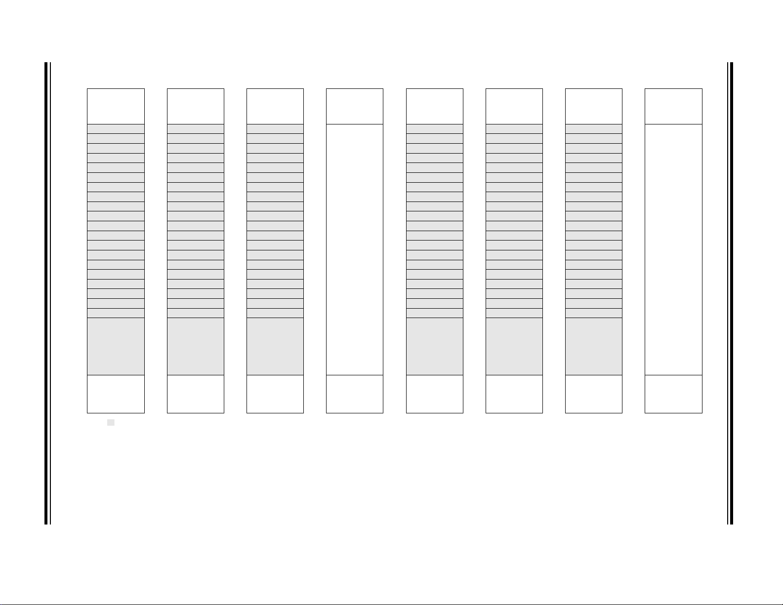
TABLE 3-3: PIC12(L)F1612 MEMORY MAP, BANK 1-7
BANK 0 BANK 1 BANK 2 BANK 3 BANK 4 BANK 5 BANK 6 BANK 7
000h
Core Registers
(Ta bl e 3- 2 )
00Bh 08Bh 10Bh 18Bh 20Bh 28Bh 30Bh 38Bh
00Ch PORTA 08Ch TRISA 10Ch LATA 18Ch ANSELA 20Ch WPUA 28Ch ODCONA 30Ch SLRCONA 38Ch INLVLA
00Dh
00Eh
00Fh
010h
011h PIR1 091h PIE1 111h CM1CON0 191h PMADRL 211h
012h PIR2 092h PIE2 112h CM1CON1 192h PMADRH 212h
013h PIR3 093h PIE3 113h
014h PIR4 094h PIE4 114h
015h TMR0 095h OPTION_REG 115h CMOUT 195h PMCON1 215h
016h
017h
018h
019h
01Ah
01Bh
01Ch
01Dh
01Eh
01Fh
020h
— 08Dh — 10Dh — 18Dh — 20Dh — 28Dh — 30Dh — 38Dh —
—08Eh—10Eh—18Eh—20Eh—28Eh—30Eh—38Eh—
—08Fh—10Fh—18Fh—20Fh—28Fh—30Fh—38Fh—
—090h—110h—190h—210h—290h
TMR1L 096h PCON 116h BORCON 196h PMCON2 216h
TMR1H 097h
T1CON 098h OSCTUNE 118h
T1GCON 099h OSCCON 119h
TMR2 09Ah OSCSTAT 11Ah
PR2 09BhADRESL11Bh
T2CON 09Ch ADRESH 11Ch
T2HLT
T2CLKCON
T2RST
080h
Core Registers
(Ta bl e 3- 2 )
— 117h FVRCON 197h VREGCON 217h
09Dh ADCON0 11Dh APFCON 19Dh
09Eh ADCON1 11Eh
09Fh ADCON2 11Fh
0A0h
100h
120h
Core Registers
(Table 3-2)
— 193h PMDATL 213h
— 194h PMDATH 214h
DAC1CON0
DAC1CON1
—19Ah
—19Bh
ZCD1CON
—
—19Fh
180h
198h
199h
19Ch
19Eh
1A0h
Core Registers
(Table 3-2)
—218h
—
—
—
—
—
—
—
200h
219h
21Ah
21Bh
21Ch
21Dh
21Eh
21Fh
220h
Core Registers
(Table 3-2)
—
—
—
—
—
—
—
—
—299h
—29Ah
—29Bh
— 29Ch — 31Ch
—
—
—
280h
Core Registers
(Table 3-2)
—
291h CCP1RL 311h
292h CCP1RH 312h
293h CCP1CON 313h
294h CCP1CAP 314h
295h
296h
297h
298h
29Dh
29Eh CCPTMRS 31Eh
29Fh
2A0h
—
— 316h — 396h
— 317h — 397h
CCP2RL
CCP2RH
CCP2CON
CCP2CAP
—
—
300h
Core Registers
(Table 3-2)
310h
315h
318h
319h — 399h
31Ah —39Ah—
31Bh
31Dh
31Fh
320h
— 390h —
—
—
—
—
—
— 398h
—
—
—
—
—
380h
Core Registers
(Table 3-2)
391h IOCAP
392h IOCAN
393h
394h
395h
39Bh
39Ch
39Dh
39Eh
39Fh
3A0h
IOCAF
—
—
—
—
—
—
—
—
—
—
—
PIC12(L)F1612/16(L)F1613
General
Purpose
Register
80 Bytes
06Fh
070h
Common RAM
07Fh 0FFh 17Fh 1FFh 27Fh 2FFh 37Fh 3FFh
Legend: = Unimplemented data memory locations, read as ‘0’.
0EFh
0F0h
General
Purpose
Register
80 Bytes
Common RAM
(Accesses
70h – 7Fh)
General
Purpose
Register
80 Bytes
16Fh 1EFh 26Fh 2EFh
170h
Common RAM
(Accesses
70h – 7Fh)
1F0h
Unimplemented
Read as ‘0’
Common RAM
(Accesses
70h – 7Fh)
270h
Unimplemented
Read as ‘0’
Common RAM
(Accesses
70h – 7Fh)
2F0h
Unimplemented
Read as ‘0’
Common RAM
(Accesses
70h – 7Fh)
Unimplemented
Read as ‘0’
36Fh 3EFh
370h
Common RAM
(Accesses
70h – 7Fh)
3F0h
Unimplemented
Read as ‘0’
Common RAM
(Accesses
70h – 7Fh)
Page 22

DS40001737A-page 22 Preliminary 2014 Microchip Technology Inc.
TABLE 3-4: PIC16(L)F1613 MEMORY MAP, BANK 1-7
PIC12(L)F1612/16(L)F1613
BANK 0 BANK 1 BANK 2 BANK 3 BANK 4 BANK 5 BANK 6 BANK 7
000h
Core Registers
(Ta bl e 3- 2 )
00Bh 08Bh 10Bh 18Bh 20Bh 28Bh 30Bh 38Bh
00Ch PORTA 08Ch TRISA 10Ch LATA 18Ch ANSELA 20Ch WPUA 28Ch ODCONA 30Ch SLRCONA 38Ch INLVLA
00Dh
00Eh PORTC 08Eh TRISC 10Eh LATC 18Eh ANSELC 20Eh WPUC 28Eh ODCONC 30Eh SLRCONC 38Eh INLVLC
00Fh —08Fh—10Fh—18Fh—20Fh—28Fh—30Fh—38Fh—
010h
011h PIR1 091h PIE1 111h CM1CON0 191h PMADRL 211h
012h PIR2 092h PIE2 112h CM1CON1 192h PMADRH 212h
013h PIR3 093h PIE3 113h CM2CON0 193h PMDATL 213h
014h PIR4 094h PIE4 114h CM2CON1 194h PMDATH 214h
015h TMR0 095h OPTION_REG 115h CMOUT 195h PMCON1 215h
016h
017h
018h
019h
01Ah
01Bh
01Ch
01Dh
01Eh
01Fh
020h
— 08Dh — 10Dh — 18Dh — 20Dh — 28Dh — 30Dh — 38Dh —
—090h—110h—190h—210h—290h
TMR1L 096h PCON 116h BORCON 196h PMCON2 216h
TMR1H 097h
T1CON 098h OSCTUNE 118h
T1GCON 099h OSCCON 119h
TMR2 09Ah OSCSTAT 11Ah
PR2 09BhADRESL11Bh
T2CON 09Ch ADRESH 11Ch
T2HLT
T2CLKCON
T2RST
080h
Core Registers
(Ta bl e 3- 2 )
— 117h FVRCON 197h VREGCON 217h
09Dh ADCON0 11Dh APFCON 19Dh
09Eh ADCON1 11Eh
09Fh ADCON2 11Fh
0A0h
100h
120h
Core Registers
(Table 3-2)
DAC1CON0
DAC1CON1
—19Ah
—19Bh
ZCD1CON
—
—19Fh
180h
198h
199h
19Ch
19Eh
1A0h
Core Registers
(Table 3-2)
—218h
—
—
—
—
—
—
—
200h
219h
21Ah
21Bh
21Ch
21Dh
21Eh
21Fh
220h
Core Registers
(Table 3-2)
—
—
—
—
—
—
—
—
—299h
—29Ah
—29Bh
— 29Ch — 31Ch
—
—
—
280h
Core Registers
(Table 3-2)
—
291h CCPR1L 311h
292h CCPR1H 312h
293h CCP1CON 313h
294h CCP1CAP 314h
295h
296h
297h
298h
29Dh
29Eh CCPTMRS 31Eh
29Fh
2A0h
—
— 316h — 396h
— 317h — 397h IOCCP
CCPR2L
CCPR2H
CCP2CON
CCP2CAP
—
—
300h
Core Registers
(Table 3-2)
310h
315h
318h
319h — 399h IOCCF
31Ah —39Ah—
31Bh
31Dh
31Fh
320h
— 390h —
—
—
—
—
—
— 398h IOCCN
—
—
—
—
—
380h
Core Registers
(Table 3-2)
391h IOCAP
392h IOCAN
393h
394h
395h
39Bh
39Ch
39Dh
39Eh
39Fh
3A0h
IOCAF
—
—
—
—
—
—
—
—
General
Purpose
Register
80 Bytes
06Fh
070h
Common RAM
07Fh 0FFh 17Fh 1FFh 27Fh 2FFh 37Fh 3FFh
Legend: = Unimplemented data memory locations, read as ‘0’.
0EFh
0F0h
General
Purpose
Register
80 Bytes
Common RAM
(Accesses
70h – 7Fh)
General
Purpose
Register
80 Bytes
16Fh 1EFh 26Fh 2EFh
170h
Common RAM
(Accesses
70h – 7Fh)
1F0h
Unimplemented
Read as ‘0’
Common RAM
(Accesses
70h – 7Fh)
270h
Unimplemented
Read as ‘0’
Common RAM
(Accesses
70h – 7Fh)
2F0h
Unimplemented
Read as ‘0’
Common RAM
(Accesses
70h – 7Fh)
Unimplemented
Read as ‘0’
36Fh 3EFh
370h
Common RAM
(Accesses
70h – 7Fh)
3F0h
Unimplemented
Read as ‘0’
Common RAM
(Accesses
70h – 7Fh)
Page 23

2014 Microchip Technology Inc. Preliminary DS40001737A-page 23
TABLE 3-5: PIC12(L)F1612/16(L)F1613 MEMORY MAP, BANK 8-23
BANK 8 BANK 9 BANK 10 BANK 11 BANK 12 BANK 13 BANK 14 BANK 15
400h
Core Registers
(Ta bl e 3- 2 )
40Bh
40Ch
40Dh
40Eh
40Fh
410h
411h
412h
413h TMR4 493h
414h PR4 494h
415h T4CON 495h
416h T4HLT 496h
417h T4CLKCON 497h
418h T4RST 498h
419h
41Ah TMR6 49Ah
41Bh PR6 49Bh
41Ch T6CON 49Ch
41Dh T6HLT 49Dh
41Eh T6CLKCON 49Eh
41Fh T6RST 49Fh
420h
— 48Ch — 50Ch — 58Ch — 60Ch — 68Ch — 70Ch — 78Ch —
— 48Dh — 50Dh — 58Dh — 60Dh — 68Dh — 70Dh — 78Dh —
—48Eh—50Eh—58Eh—60Eh—68Eh—70Eh—78Eh—
—48Fh—50Fh—58Fh—60Fh—68Fh—70Fh—78Fh—
—490h—510h—590h—610h—690h— 710h — 790h —
—491h—511h—591h—611h—691h
—492h—512h—592h—612h—692h
—499h—519h—599h—619h—699h
480h
48Bh
4A0h
Core Registers
(Ta bl e 3- 2 )
—513h—593h—613h—693h
—514h—594h—614h—694h
—515h—595h—615h—695h
—516h—596h—616h—696h
—517h—597h—617h—697h
—518h—598h—618h—698h
—51Ah—59Ah—61Ah—69Ah
—51Bh—59Bh—61Bh—69Bh— 71Bh SCANHADRH 79Bh —
— 51Ch — 59Ch — 61Ch — 69Ch — 71Ch SCANCON0 79Ch —
— 51Dh — 59Dh — 61Dh — 69Dh — 71Dh SCANTRIG 79Dh —
—51Eh—59Eh—61Eh—69Eh—71Eh—79Eh—
—51Fh—59Fh—61Fh—69Fh—71Fh—79Fh—
500h
50Bh
520h
Core Registers
(Table 3-2)
580h
58Bh
5A0h
Core Registers
(Table 3-2)
600h
60Bh
620h
Core Registers
(Table 3-2)
680h
68Bh
6A0h
Core Registers
(Table 3-2)
CWG1DBR
CWG1DBF
CWG1AS0
CWG1AS1
CWG1OCON0
CWG1CON0
CWG1CON1
CWG1OCON1
CWG1CLKCON
CWG1ISM
700h
Core Registers
(Table 3-2)
70Bh
711h WDTCON0 791h CRCDATL
712h WDTCON1 792h CRCDATH
713h WDTPSL 793h CRCACCL
714h WDTPSH 794h CRCACCH
715h WDTTMR 795h CRCSHIFTL
716h — 796h CRCSHIFTH
717h — 797h CRCXORL
718h SCANLADRL 798h CRCXORH
719h SCANLADRH 799h CRCCON0
71Ah SCANHADRL 79Ah CRCCON1
720h
780h
78Bh
7A0h
Core Registers
(Table 3-2)
PIC12(L)F1612/16(L)F1613
Unimplemented
Read as ‘0’
46Fh 4EFh 56Fh 5EFh 66Fh 6EFh 76Fh 7EFh
470h
Accesses
70h – 7Fh
47Fh 4FFh 57Fh 5FFh 67Fh 6FFh 77Fh 7FFh
4F0h
Unimplemented
Read as ‘0’
Accesses
70h – 7Fh
570h
Unimplemented
Read as ‘0’
Accesses
70h – 7Fh
5F0h
Unimplemented
Read as ‘0’
Accesses
70h – 7Fh
670h
Unimplemented
Read as ‘0’
Accesses
70h – 7Fh
6F0h
Unimplemented
Read as ‘0’
Accesses
70h – 7Fh
770h
Unimplemented
Read as ‘0’
7F0h
Accesses
70h – 7Fh
BANK 16 BANK 17 BANK 18 BANK 19 BANK 20 BANK 21 BANK 22 BANK 23
800h
Core Registers
(Ta bl e 3- 2 )
80Bh
80Ch
Unimplemented
Read as ‘0’
86Fh 8EFh 96Fh
870h
87Fh 8FFh 97Fh 9FFh A7Fh AFFh B7Fh BFFh
Legend: = Unimplemented data memory locations, read as ‘0’.
Accesses
70h – 7Fh
880h
88Bh
88Ch
8F0h
Core Registers
(Ta bl e 3- 2 )
Unimplemented
Read as ‘0’
Accesses
70h – 7Fh
900h
90Bh
90Ch
970h
Core Registers
(Table 3-2)
Unimplemented
Read as ‘0’
Accesses
70h – 7Fh
980h
98Bh
98Ch
9EFh
9F0h
Core Registers
(Table 3-2)
Unimplemented
Read as ‘0’
Accesses
70h – 7Fh
A00h
A0Bh
A0Ch
A6Fh
A70h
Core Registers
(Table 3-2)
Unimplemented
Read as ‘0’
Accesses
70h – 7Fh
A80h
A8Bh
A8Ch
AEFh
AF0h
Core Registers
(Table 3-2)
Unimplemented
Read as ‘0’
Accesses
70h – 7Fh
B00h
B0Bh
B0Ch
B6Fh
B70h
Core Registers
(Table 3-2)
Unimplemented
Read as ‘0’
Accesses
70h – 7Fh
B80h
B8Bh
B8Ch
BEFh
BF0h
Unimplemented
Read as ‘0’
Accesses
70h – 7Fh
Core Registers
(Table 3-2)
Unimplemented
Read as ‘0’
Accesses
70h – 7Fh
Page 24
DS40001737A-page 24 Preliminary 2014 Microchip Technology Inc.
Legend: = Unimplemented data memory locations, read as ‘0’.
BANK 24 BANK 25 BANK 26 BANK 27 BANK 28 BANK 29 BANK 30 BANK 31
C00h
C0Bh
Core Registers
(Ta bl e 3- 2 )
C80h
C8Bh
Core Registers
(Ta bl e 3- 2 )
D00h
D0Bh
Core Registers
(Ta bl e 3- 2 )
D80h
D8Bh
Core Registers
(Ta bl e 3- 2 )
E00h
E0Bh
Core Registers
(Ta bl e 3- 2 )
E80h
E8Bh
Core Registers
(Ta bl e 3- 2 )
F00h
F0Bh
Core Registers
(Ta bl e 3- 2 )
F80h
F8Bh
Core Registers
(Ta bl e 3- 2 )
C0Ch
—C8Ch—D0Ch—D8Ch
See Tab l e 3- 7 for
register mapping
details
E0Ch
—E8Ch—F0Ch—F8Ch
See Tab l e 3- 8 for
register mapping
details
C0Dh —C8Dh—D0Dh— D8Dh E0Dh —E8Dh—F0Dh—F8Dh
C0Eh
—C8Eh—D0Eh—D8Eh E0Eh—E8Eh—F0Eh—F8Eh
C0Fh
—C8Fh—D0Fh—D8Fh E0Fh—E8Fh—F0Fh—F8Fh
C10h
—C90h—D10h—D90h E10h—E90h—F10h—F90h
C11h
—C91h—D11h—D91h E11h—E91h—F11h—F91h
C12h
—C92h—D12h—D92h E12h—E92h—F12h—F92h
C13h
—C93h—D13h—D93h E13h—E93h—F13h—F93h
C14h
—C94h—D14h—D94h E14h—E94h—F14h—F94h
C15h
—C95h—D15h—D95h E15h—E95h—F15h—F95h
C16h
—C96h—D16h—D96h E16h—E96h—F16h—F96h
C17h
—C97h—D17h—D97h E17h—E97h—F17h—F97h
C18h
—C98h—D18h—D98h E18h—E98h—F18h—F98h
C19h
—C99h—D19h—D99h E19h—E99h—F19h—F99h
C1Ah
—C9Ah—D1Ah—D9Ah E1Ah—E9Ah—F1Ah—F9Ah
C1Bh
—C9Bh—D1Bh—D9Bh E1Bh—E9Bh—F1Bh—F9Bh
C1Ch
—C9Ch—D1Ch— D9Ch E1Ch —E9Ch—F1Ch—F9Ch
C1Dh
—C9Dh—D1Dh— D9Dh E1Dh —E9Dh—F1Dh—F9Dh
C1Eh
—C9Eh—D1Eh—D9Eh E1Eh—E9Eh—F1Eh—F9Eh
C1Fh
—C9Fh—D1Fh—D9Fh E1Fh—E9Fh—F1Fh—F9Fh
C20h
Unimplemented
Read as ‘0’
CA0h
Unimplemented
Read as ‘0’
D20h
Unimplemented
Read as ‘0’
DA0h E20h
Unimplemented
Read as ‘0’
EA0h
Unimplemented
Read as ‘0’
F20h
Unimplemented
Read as ‘0’
FA0h
C6Fh CEFh D6Fh DEFh E6Fh EEFh F6Fh FEFh
C70h
Accesses
70h – 7Fh
CF0h
Accesses
70h – 7Fh
D70h
Accesses
70h – 7Fh
DF0h
Accesses
70h – 7Fh
E70h
Accesses
70h – 7Fh
EF0h
Accesses
70h – 7Fh
F70h
Accesses
70h – 7Fh
FF0h
Accesses
70h – 7Fh
CFFh
CFFh D7Fh DFFh E7Fh EFFh F7Fh FFFh
TABLE 3-6: PIC12(L)F1612/16(L)F1613 MEMORY MAP, BANK 24-31
PIC12(L)F1612/16(L)F1613
Page 25
PIC12(L)F1612/16(L)F1613
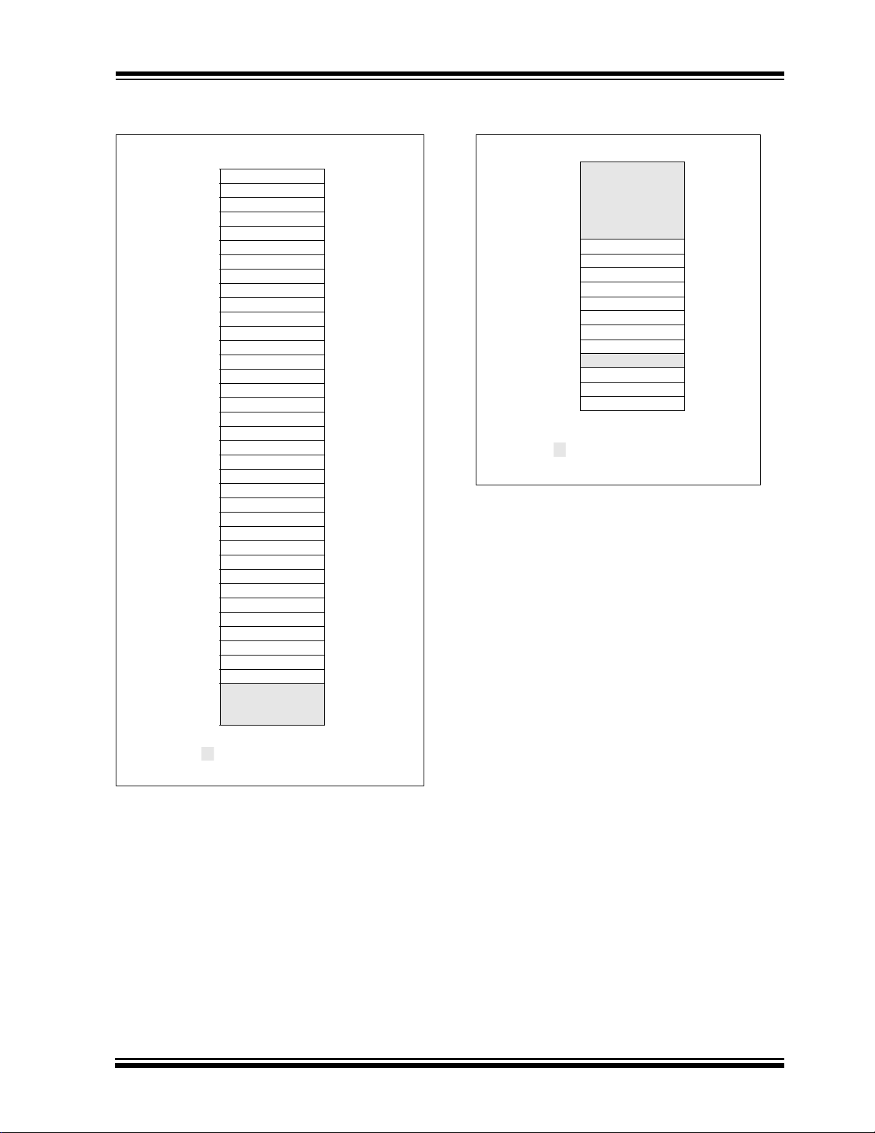
Bank 27
D8Ch
SMT1TMRL
D8Dh
SMT1TMRH
D8Eh
SMT1TMRU
D8Fh
SMT1CPRL
D90h
SMT1CPRH
D91h
SMT1CPRU
D92h
SMT1CPWL
D93h
SMT1CPWH
D94h
SMT1CPWU
D95h
SMT1PRL
D96h
SMT1PRH
D97h
SMT1PRU
D98h
SMT1CON0
D99h
SMT1CON1
D9Ah
SMT1STAT
D9Bh
SMT1CLK
D9Ch
SMT1SIG
D9Dh
SMT1WIN
D9Eh
SMT2TMRL
D9Fh
SMT2TMRH
DA0h
SMT2TMRU
DA1h
SMT2CPRL
DA2h
SMT2CPRH
DA3h
SMT2CPRU
DA4h
SMT2CPWL
DA5h
SMT2CPWH
DA6h
SMT2CPWU
DA7h
SMT2PRL
DA8h
SMT2PRH
DA9h
SMT2PRU
DAAh
SMT2CON0
DABh
SMT2CON1
DACh
SMT2STAT
DADh
SMT2CLK
DAEh
SMT2SIG
DAFh
SMT2WIN
DB0h
—
DEFh
Legend: = Unimplemented data memory locations,
read as ‘0’.
Bank 31
F8Ch
FE3h
Unimplemented
Read as ‘0’
FE4h
STATUS_SHAD
FE5h
WREG_SHAD
FE6h
BSR_SHAD
FE7h
PCLATH_SHAD
FE8h
FSR0L_SHAD
FE9h
FSR0H_SHAD
FEAh
FSR1L_SHAD
FEBh
FSR1H_SHAD
FECh
—
FEDh
STKPTR
FEEh
TOSL
FEFh
TOSH
Legend: = Unimplemented data memory locations,
read as ‘0’.
TABLE 3-7: PIC12(L)F1612/16(L)F1613
MEMORY MAP, BANK 27
2014 Microchip Technology Inc. Preliminary DS40001737A-page 25
TABLE 3-8: PIC12(L)F1612/16(L)F1613
MEMORY MAP, BANK 31
Page 26
PIC12(L)F1612/16(L)F1613
3.2.6 CORE FUNCTION REGISTERS SUMMARY
The Core Function registers listed in Ta bl e 3 -9 can be
addressed from any Bank.
TABLE 3-9: CORE FUNCTION REGISTERS SUMMARY
Addr Name Bit 7 Bit 6 Bit 5 Bit 4 Bit 3 Bit 2 Bit 1 Bit 0
Bank 0-31
x00h or
INDF0
x80h
x01h or
INDF1
x81h
x02h or
PCL Program Counter (PC) Least Significant Byte 0000 0000 0000 0000
x82h
x03h or
STATUS
x83h
x04h or
FSR0L Indirect Data Memory Address 0 Low Pointer 0000 0000 uuuu uuuu
x84h
x05h or
FSR0H Indirect Data Memory Address 0 High Pointer 0000 0000 0000 0000
x85h
x06h or
FSR1L Indirect Data Memory Address 1 Low Pointer 0000 0000 uuuu uuuu
x86h
x07h or
FSR1H Indirect Data Memory Address 1 High Pointer 0000 0000 0000 0000
x87h
x08h or
BSR
x88h
x09h or
WREG Working Register 0000 0000 uuuu uuuu
x89h
x0Ah or
PCLATH
x8Ah
x0Bh or
INTCON GIE PEIE TMR0IE INTE IOCIE TMR0IF INTF IOCIF 0000 0000 0000 0000
x8Bh
Legend: x = unknown, u = unchanged, q = value depends on condition, - = unimplemented, read as ‘0’, r = reserved.
Addressing this location uses contents of FSR0H/FSR0L to address data memory
(not a physical register)
Addressing this location uses contents of FSR1H/FSR1L to address data memory
(not a physical register)
— — —TOPD ZDCC---1 1000 ---q quuu
— — —BSR<4:0>---0 0000 ---0 0000
— Write Buffer for the upper 7 bits of the Program Counter -000 0000 -000 0000
Shaded locations are unimplemented, read as ‘0’.
Val ue o n
POR, BOR
xxxx xxxx uuuu uuuu
xxxx xxxx uuuu uuuu
Value on all
other Resets
DS40001737A-page 26 Preliminary 2014 Microchip Technology Inc.
Page 27
2014 Microchip Technology Inc. Preliminary DS40001737A-page 27
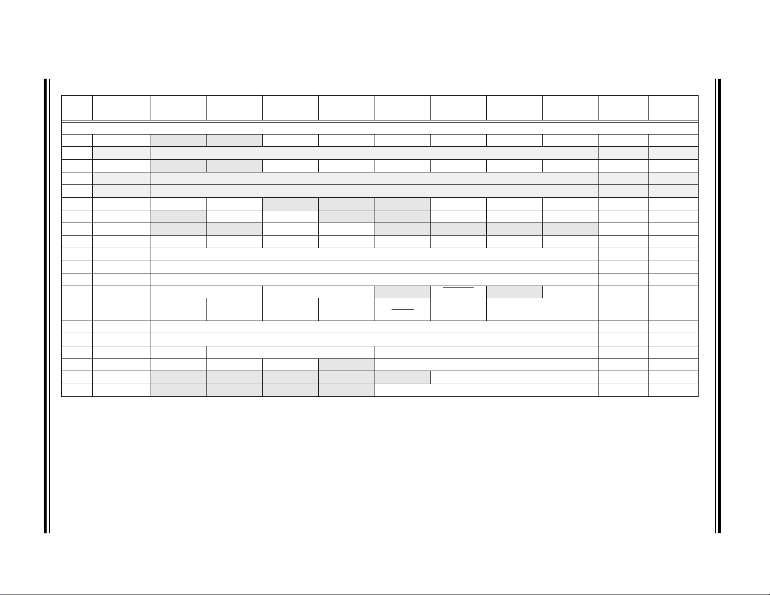
TABLE 3-10: SPECIAL FUNCTION REGISTER SUMMARY
Addr Name Bit 7 Bit 6 Bit 5 Bit 4 Bit 3 Bit 2 Bit 1 Bit 0
Bank 0
00Ch PORTA
00Dh
00Eh PORTC
00Fh
010h
011h PIR1 TMR1GIF ADIF
012h PIR2
013h PIR3
014h PIR4 SCANIF CRCIF SMT2PWAIF SMT2PRAIF SMT2IF SMT1PWAIF SMT1PRAIF SMT1IF 0000 0000 0000 0000
015h TMR0 Holding Register for the 8-bit Timer0 Count xxxx xxxx uuuu uuuu
016h TMR1L Holding Register for the Least Significant Byte of the 16-bit TMR1 Count xxxx xxxx uuuu uuuu
017h TMR1H Holding Register for the Most Significant Byte of the 16-bit TMR1 Count xxxx xxxx uuuu uuuu
018h T1CON TMR1CS<1:0> T1CKPS<1:0>
019h T1GCON TMR1GE T1GPOL T1GTM T1GSPM T1GGO/
01Ah TMR2 Timer2 Module Register 0000 0000 0000 0000
01Bh PR2 Timer2 Period Register 1111 1111 1111 1111
01Ch T2CON ON CKPS<2:0> OUTPS<3:0> 0000 0000 0000 0000
01Dh T2HLT PSYNC CKPOL CKSYNC
01Eh T2CLKCON
01Fh T2RST
Legend: x = unknown, u = unchanged, q = value depends on condition, - = unimplemented, r = reserved. Shaded locations are unimplemented, read as ‘0’.
Note 1: PIC12F1612/16F1613 only.
— Unimplemented — —
(4)
— Unimplemented — —
— Unimplemented — —
2: Unimplemented, read as ‘1’.
3: PIC12(L)F1612 only.
4: PIC16(L)F1613 only.
— — RA5 RA4 RA3 RA2 RA1 RA0 --xx xxxx --xx xxxx
— — RC5 RC4 RC3 RC2 RC1 RC0 --xx xxxx --xx xxxx
—C2IF
— —CWGIFZCDIF — — — — --00 ---- --00 ----
— — — — — T2CS<2:0> ---- -000 ---- -000
— — — — RSEL<3:0> ---- 0000 ---- 0000
(4)
— — — CCP1IF TMR2IF TMR1IF 00-- -000 00-- -000
C1IF — — TMR6IF TMR4IF CCP2IF -00- -000 -00- -000
—T1SYNC—TMR1ON0000 -0-0 uuuu -u-u
T1GVAL T1GSS<1:0> 0000 0x00 uuuu uxuu
DONE
—MODE<3:0>000- 0000 000- 0000
Val ue o n
POR, BOR
Value on all
other Resets
PIC12(L)F1612/16(L)F1613
Page 28
DS40001737A-page 28 Preliminary 2014 Microchip Technology Inc.
TABLE 3-10: SPECIAL FUNCTION REGISTER SUMMARY (CONTINUED)
Addr Name Bit 7 Bit 6 Bit 5 Bit 4 Bit 3 Bit 2 Bit 1 Bit 0
Bank 1
08Ch TRISA
08Dh
08Eh TRISC
08Fh
090h
091h PIE1 TMR1GIE ADIE
092h PIE2
093h PIE3
094h PIE4 SCANIE CRCIE SMT2PWAIE SMT2PRAIE SMT2IE SMT1PWAIE SMT1PRAIE SMT1IE 0000 0000 0000 0000
095h OPTION_REG WPUEN
096h PCON STKOVF STKUNF WDTWV
097h
098h OSCTUNE
099h OSCCON SPLLEN IRCF<3:0>
09Ah OSCSTAT
09Bh ADRESL ADC Result Register Low xxxx xxxx uuuu uuuu
09Ch ADRESH ADC Result Register High xxxx xxxx uuuu uuuu
09Dh ADCON0
09Eh ADCON1 ADFM ADCS<2:0>
09Fh ADCON2 TRIGSEL<3:0>
Legend: x = unknown, u = unchanged, q = value depends on condition, - = unimplemented, r = reserved. Shaded locations are unimplemented, read as ‘0’.
Note 1: PIC12F1612/16F1613 only.
— Unimplemented — —
(4)
— Unimplemented — —
— Unimplemented — —
— Unimplemented — —
2: Unimplemented, read as ‘1’.
3: PIC12(L)F1612 only.
4: PIC16(L)F1613 only.
— — TRISA5 TRISA4 —
— — TRISC5 TRISC4 TRISC3 TRISC2 TRISC1 TRISC0 --11 1111 --11 1111
—C2IE
— — CWGIE ZCDIE — — — — --00 ---- --00 ----
— — TUN<5:0> --00 0000 --00 0000
— PLLR — HFIOFR HFIOFL MFIOFR LFIOFR HFIOFS -0-0 0000 -q-q qqqq
— CHS<4:0> GO/DONE ADON -000 0000 -000 0000
(4)
INTEDG TMR0CS TMR0SE PSA PS<2:0> 1111 1111 1111 1111
— — — CCP1IE TMR2IE TMR1IE 00-- -000 00-- -000
C1IE — — TMR6IE TMR4IE CCP2IE -00- -000 -00- -000
RWDT RMCLR RI POR BOR 00-1 11qq qq-q qquu
(2)
— — ADPREF<1:0> 0000 --00 0000 --00
— — — — 0000 ---- 0000 ----
TRISA2 TRISA1 TRISA0 --11 1111 --11 1111
—SCS<1:0>0011 1-00 0011 1-00
Val ue o n
POR, BOR
Value on all
other Resets
PIC12(L)F1612/16(L)F1613
Page 29
2014 Microchip Technology Inc. Preliminary DS40001737A-page 29
TABLE 3-10: SPECIAL FUNCTION REGISTER SUMMARY (CONTINUED)
Addr Name Bit 7 Bit 6 Bit 5 Bit 4 Bit 3 Bit 2 Bit 1 Bit 0
Bank 2
10Ch LATA
10Dh
10Eh LATC
10Fh
110h
111h CM1CON0 C1ON C1OUT C1OE C1POL
112h CM1CON1 C1INTP C1INTN C1PCH<1:0>
113h CM2CON0
114h CM2CON1
115h CMOUT
116h BORCON SBOREN BORFS
117h FVRCON FVREN FVRRDY TSEN TSRNG CDAFVR<1:0> ADFVR<1:0> 0q00 0000 0q00 0000
118h DAC1CON0 DAC1EN
119h DAC1CON1 DAC1R<7:0> 0000 0000 0000 0000
11Ah
11Bh
11Ch ZCD1CON ZCD1EN ZCD1OE ZCD1OUT ZCD1POL
11Dh APFC ON
11Eh
11Fh
Legend: x = unknown, u = unchanged, q = value depends on condition, - = unimplemented, r = reserved. Shaded locations are unimplemented, read as ‘0’.
Note 1: PIC12F1612/16F1613 only.
— Unimplemented — —
(4)
— Unimplemented — —
— Unimplemented — —
(4)
(4)
— Unimplemented — —
— Unimplemented — —
— Unimplemented — —
— Unimplemented — —
2: Unimplemented, read as ‘1’.
3: PIC12(L)F1612 only.
4: PIC16(L)F1613 only.
— —LATA5LATA4— LATA2 LATA1 LATA0 --xx -xxx --uu -uuu
— — LAT C5 LATC4 LATC3 LAT C2 LATC1 LAT C0 --xx xxxx --uu uuuu
— C1SP C1HYS C1SYNC 0000 -100 0000 -100
— C1NCH<2:0> 0000 -000 0000 -000
C2ON C2OUT C2OE C2POL — C2SP C2HYS C2SYNC 0000 -100 0000 -100
C2INTP C2INTN C2PCH<1:0> — C2NCH<2:0> 0000 -000 0000 -000
— — — — — — MC2OUT MC1OUT ---- --00 ---- --00
— — — — — BORRDY 10-- ---q uu-- ---u
—DAC1OE1— DAC1PSS<1:0> — — 0-0- 00-- 0-0- 00--
— — ZCD1INTP ZCD1INTN 0000 --00 0000 --00
(4)
CCP1SEL
— CWGASEL
(3)
CWGBSEL
(3)
—T1GSEL— CCP2SEL
Val ue o n
POR, BOR
(3)
-00- 0-00 -00- 0-00
Value on all
other Resets
PIC12(L)F1612/16(L)F1613
Page 30
DS40001737A-page 30 Preliminary 2014 Microchip Technology Inc.
TABLE 3-10: SPECIAL FUNCTION REGISTER SUMMARY (CONTINUED)
Addr Name Bit 7 Bit 6 Bit 5 Bit 4 Bit 3 Bit 2 Bit 1 Bit 0
Bank 3
18Ch ANSELA
18Dh
18Eh ANSELC
18Fh
190h
191h PMADRL Flash Program Memory Address Register Low Byte 0000 0000 0000 0000
192h PMADRH
193h PMDATL Flash Program Memory Read Data Register Low Byte xxxx xxxx uuuu uuuu
194h PMDATH
195h PMCON1
196h PMCON2 Flash Program Memory Control Register 2 0000 0000 0000 0000
197h VREGCON
Bank 4
20Ch WPUA
20Dh
20Eh WPUC
Legend: x = unknown, u = unchanged, q = value depends on condition, - = unimplemented, r = reserved. Shaded locations are unimplemented, read as ‘0’.
Note 1: PIC12F1612/16F1613 only.
— Unimplemented — —
— Unimplemented — —
— Unimplemented — —
198h
— Unimplemented — —
to
19Fh
— Unimplemented — —
20Fh
— Unimplemented — —
to
21Fh
2: Unimplemented, read as ‘1’.
3: PIC12(L)F1612 only.
4: PIC16(L)F1613 only.
(4)
(1)
(4)
— — —ANSA4— ANSA2 ANSA1 ANSA0 ---1 -111 ---1 -111
— — — — ANSC3 ANSC2 ANSC1 ANSC0 ---- 1111 ---- 1111
(2)
—
— — Flash Program Memory Read Data Register High Byte --xx xxxx --uu uuuu
(2)
—
— — — — — —VREGPMReserved ---- --01 ---- --01
— — WPUA5 WPUA4 WPUA3 WPUA2 WPUA1 WPUA0 --11 1111 --11 1111
— — WPUC5 WPUC4 WPUC3 WPUC2 WPUC1 WPUC0 --11 1111 --11 1111
Flash Program Memory Address Register High Byte 1000 0000 1000 0000
CFGS LWLO FREE WRERR WREN WR RD 1000 x000 1000 q000
Val ue o n
POR, BOR
Value on all
other Resets
PIC12(L)F1612/16(L)F1613
Page 31

2014 Microchip Technology Inc. Preliminary DS40001737A-page 31
TABLE 3-10: SPECIAL FUNCTION REGISTER SUMMARY (CONTINUED)
Addr Name Bit 7 Bit 6 Bit 5 Bit 4 Bit 3 Bit 2 Bit 1 Bit 0
Bank 5
28Ch ODCONA
28Dh
28Eh ODCONC
28Fh
290h
291h CCP1RL Capture/Compare/PWM 1 Register (LSB) xxxx xxxx uuuu uuuu
292h CCP1RH Capture/Compare/PWM 1 Register (MSB) xxxx xxxx uuuu uuuu
293h CCP1CON EN OE OUT FMT MODE<3:0> 0000 0000 0000 0000
294h CCP1CAP
298h CCP2RL Capture/Compare/PWM 2 Register (LSB) xxxx xxxx uuuu uuuu
299h CCP2RH Capture/Compare/PWM 2 Register (MSB) xxxx xxxx uuuu uuuu
29Ah CCP2CON EN OE OUT FMT MODE<3:0> 0000 0000 0000 0000
29Bh CCP2CAP
29Ch
29Dh
29Eh CCPTMRS
29Fh
Bank 6
30Ch SLRCONA
30Dh
30Eh SLRCONC
30Fh
—
31Fh
Legend: x = unknown, u = unchanged, q = value depends on condition, - = unimplemented, r = reserved. Shaded locations are unimplemented, read as ‘0’.
Note 1: PIC12F1612/16F1613 only.
— Unimplemented — —
— Unimplemented — —
— Unimplemented — —
295h
—
— Unimplemented — —
297h
— Unimplemented — —
— Unimplemented — —
— Unimplemented — —
— Unimplemented — —
— Unimplemented — —
2: Unimplemented, read as ‘1’.
3: PIC12(L)F1612 only.
4: PIC16(L)F1613 only.
(4)
(4)
— — ODA5 ODA4 — ODA2 ODA1 ODA0 --00 -000 --00 -000
— — ODC5 ODC4 ODC3 ODC2 ODC1 ODC0 --00 0000 --00 0000
— — — — — —CTS<1:0>---- --00 ---- --00
— — — — — —CTS<1:0>---- --00 ---- --00
— — — — C2TSEL<1:0> C1TSEL<1:0> ---- 0000 ---- 0000
— —SLRA5SLRA4— SLRA2 SLRA1 SLRA0 --00 -000 --00 -000
— — SLRC5 SLRC4 SLRC3 SLRC2 SLRC1 SLRC0 --00 0000 --00 0000
Val ue o n
POR, BOR
Value on all
other Resets
PIC12(L)F1612/16(L)F1613
Page 32

DS40001737A-page 32 Preliminary 2014 Microchip Technology Inc.
TABLE 3-10: SPECIAL FUNCTION REGISTER SUMMARY (CONTINUED)
Addr Name Bit 7 Bit 6 Bit 5 Bit 4 Bit 3 Bit 2 Bit 1 Bit 0
Bank 7
38Ch INLVLA
38Dh
38Eh INLVLC
30Fh
390h
391h IOCAP
392h IOCAN
393h IOCAF
394h
395h
396h
397h IOCCP
398h IOCCN
399h IOCCF
Legend: x = unknown, u = unchanged, q = value depends on condition, - = unimplemented, r = reserved. Shaded locations are unimplemented, read as ‘0’.
Note 1: PIC12F1612/16F1613 only.
— Unimplemented — —
(4)
— Unimplemented — —
— Unimplemented — —
— Unimplemented — —
— Unimplemented — —
— Unimplemented — —
(4)
(4)
(4)
39Ah
— Unimplemented — —
to
39Fh
2: Unimplemented, read as ‘1’.
3: PIC12(L)F1612 only.
4: PIC16(L)F1613 only.
— — INLVLA5 INLVLA4 INLVLA3 INLVLA2 INLVLA1 INLVLA0 --11 1111 --11 1111
— — INLVLC5 INLVLC4 INLVLC3 INLVLC2 INLVLC1 INLVLC0 --11 1111 --11 1111
— — IOCAP5 IOCAP4 IOCAP3 IOCAP2 IOCAP1 IOCAP0 --00 0000 --00 0000
— — IOCAN5 IOCAN4 IOCAN3 IOCAN2 IOCAN1 IOCAN0 --00 0000 --00 0000
— — IOCAF5 IOCAF4 IOCAF3 IOCAF2 IOCAF1 IOCAF0 --00 0000 --00 0000
— — IOCCP5 IOCCP4 IOCCP3 IOCCP2 IOCCP1 IOCCP0 --00 0000 --00 0000
— — IOCCN5 IOCCN4 IOCCN3 IOCCN2 IOCCN1 IOCCN0 --00 0000 --00 0000
— — IOCCF5 IOCCF4 IOCCF3 IOCCF2 IOCCF1 IOCCF0 --00 0000 --00 0000
Val ue o n
POR, BOR
Value on all
other Resets
PIC12(L)F1612/16(L)F1613
Page 33

2014 Microchip Technology Inc. Preliminary DS40001737A-page 33
TABLE 3-10: SPECIAL FUNCTION REGISTER SUMMARY (CONTINUED)
Addr Name Bit 7 Bit 6 Bit 5 Bit 4 Bit 3 Bit 2 Bit 1 Bit 0
Bank 8
40Ch
— Unimplemented — —
to
412h
413h TMR4 Timer4 Module Register 0000 0000 0000 0000
414h PR4 Timer4 Period Register 1111 1111 1111 1111
415h T4CON ON CKPS<2:0> OUTPS<3:0> 0000 0000 0000 0000
416h T4HLT PSYNC CKPOL CKSYNC
417h T4CLKCON
418h T4RST
419h
41Ah TMR6 Timer6 Module Register 0000 0000 0000 0000
41Bh PR6 Timer6 Period Register 1111 1111 1111 1111
41Ch T6CON ON CKPS<2:0> OUTPS<3:0> 0000 0000 0000 0000
41Dh T6HLT PSYNC CKPOL CKSYNC
41Eh T6CLKCON
41Fh T6RST
Bank 9
Bank 10
Bank 11
Legend: x = unknown, u = unchanged, q = value depends on condition, - = unimplemented, r = reserved. Shaded locations are unimplemented, read as ‘0’.
Note 1: PIC12F1612/16F1613 only.
— Unimplemented — —
48Ch
— Unimplemented — —
to
49Fh
50Ch
— Unimplemented — —
to
51Fh
58Ch
to
— Unimplemented — —
59Fh
2: Unimplemented, read as ‘1’.
3: PIC12(L)F1612 only.
4: PIC16(L)F1613 only.
— — — — — T4CS<2:0> ---- -000 ---- -000
— — — — RSEL<3:0> ---- 0000 ---- 0000
— — — — — T6CS<2:0> ---- -000 ---- -000
— — — — RSEL<3:0> ---- 0000 ---- 0000
—MODE<3:0>000- 0000 000- 0000
—MODE<3:0>000- 0000 000- 0000
Val ue o n
POR, BOR
Value on all
other Resets
PIC12(L)F1612/16(L)F1613
Page 34

DS40001737A-page 34 Preliminary 2014 Microchip Technology Inc.
TABLE 3-10: SPECIAL FUNCTION REGISTER SUMMARY (CONTINUED)
Addr Name Bit 7 Bit 6 Bit 5 Bit 4 Bit 3 Bit 2 Bit 1 Bit 0
Bank 12
60Ch
— Unimplemented — —
to
61Fh
Bank 13
68Ch
to
— Unimplemented — —
690h
691h CWG1DBR
692h CWG1DBF
693h CWG1AS0 SHUTDOWN REN LSBD<1:0> LSAC<1:0>
694h CWG1AS1
695h CWG1OCON0 OVRD OVRC OVRB OVRA STRD STRC STRB STRA 0000 0000 0000 0000
696h CWG1CON0 EN LD
697h CWG1CON1
698h CWG1OCON1
699h CWG1CLKCON
69Ah CWG1ISM
69Bh
— Unimplemented — —
to
6EFh
Legend: x = unknown, u = unchanged, q = value depends on condition, - = unimplemented, r = reserved. Shaded locations are unimplemented, read as ‘0’.
Note 1: PIC12F1612/16F1613 only.
2: Unimplemented, read as ‘1’.
3: PIC12(L)F1612 only.
4: PIC16(L)F1613 only.
— —DBR<5:0>--00 0000 --00 0000
— —DBF<5:0>--xx xxxx --xx xxxx
— TMR6AS TMR4AS TMR2AS —C2AS
— — —MODE<2:0>00-- -000 00-- -000
— —IN— POLD POLC POLB POLA --x- 0000 --x- 0000
— — — —OEDOECOEBOEA---- 0000 ---- 0000
— — — — — — —CS---- ---0 ---- --0
— — — — — IS<2:0> ---- -000 ---- -000
(4)
— — 0000 00-- 0000 00--
C1AS INAS -000 -000 -000 -000
Val ue o n
POR, BOR
Value on all
other Resets
PIC12(L)F1612/16(L)F1613
Page 35

2014 Microchip Technology Inc. Preliminary DS40001737A-page 35
TABLE 3-10: SPECIAL FUNCTION REGISTER SUMMARY (CONTINUED)
Addr Name Bit 7 Bit 6 Bit 5 Bit 4 Bit 3 Bit 2 Bit 1 Bit 0
Bank 14
70Ch
— Unimplemented — —
to
710h
711h WDTCON0
712h WDTCON1
713h WDTPSL PSCNT<7:0> 0000 0000 0000 0000
714h WDTPSH PSCNT<15:8> 0000 0000 0000 0000
715h WDTTMR WDTTMR<4:0> STATE PSCNT<17:16> 0000 0000 0000 0000
716h
717h
718h SCANLADRL LADR<7:0> 0000 0000 0000 0000
719h SCANLADRH LADR<15:8> 0000 0000 0000 0000
71Ah SCANHADRL HADR<7:0> 1111 1111 1111 1111
71Bh SCANHADRH HADR<15:8> 1111 1111 1111 1111
71Ch SCANCON0 EN SCANGO BUSY INVALID INTM
71Dh SCANTRIG
71Eh
71Fh
Legend: x = unknown, u = unchanged, q = value depends on condition, - = unimplemented, r = reserved. Shaded locations are unimplemented, read as ‘0’.
Note 1: PIC12F1612/16F1613 only.
— Unimplemented — —
— Unimplemented — —
— Unimplemented — —
— Unimplemented — —
2: Unimplemented, read as ‘1’.
3: PIC12(L)F1612 only.
4: PIC16(L)F1613 only.
— —WDTPS<4:0>SEN--qq qqqq --qq qqqq
—WDTCS<2:0>— WINDOW<2:0> -qqq -qqq -qqq -qqq
— MODE<1:0> 0000 0-00 0000 0-00
— —
TSEL<1:0>
Val ue o n
POR, BOR
---- --00 ---- --00
Value on all
other Resets
PIC12(L)F1612/16(L)F1613
Page 36

DS40001737A-page 36 Preliminary 2014 Microchip Technology Inc.
TABLE 3-10: SPECIAL FUNCTION REGISTER SUMMARY (CONTINUED)
Addr Name Bit 7 Bit 6 Bit 5 Bit 4 Bit 3 Bit 2 Bit 1 Bit 0
Banks 15
78Ch
— Unimplemented — —
to
790h
791h CRCDATL DATA<7:0> xxxx xxxx xxxx xxxx
792h CRCDATH DATA<15:8> xxxx xxxx xxxx xxxx
793h CRCACCL ACC<7:0> 0000 0000 0000 0000
794h CRCACCH ACC<15:8> 0000 0000 0000 0000
795h CRCSHIFTL SHIFT<7:0> 0000 0000 0000 0000
796h CRCSHIFTH SHIFT<15:8> 0000 0000 0000 0000
797h CRCXORL X<7:1>
798h CRCXORH X<15:8> xxxx xxxX xxxx xxxX
799h CRCCON0 EN CRCGO BUSY ACCM
79Ah CRCCON1 DLEN<3:0> PLEN<3:0> 0000 0000 0000 0000
79Bh
— Unimplemented — —
to
79Fh
Bank 16-26
x0Ch/
x8Ch
—
x1Fh/
x9Fh
Legend: x = unknown, u = unchanged, q = value depends on condition, - = unimplemented, r = reserved. Shaded locations are unimplemented, read as ‘0’.
Note 1: PIC12F1612/16F1613 only.
— Unimplemented — —
2: Unimplemented, read as ‘1’.
3: PIC12(L)F1612 only.
4: PIC16(L)F1613 only.
— — SHIFTM FULL 0000 --00 0000 -00
— xxxx xxx- xxxx xxx-
Val ue o n
POR, BOR
Value on all
other Resets
PIC12(L)F1612/16(L)F1613
Page 37

2014 Microchip Technology Inc. Preliminary DS40001737A-page 37
TABLE 3-10: SPECIAL FUNCTION REGISTER SUMMARY (CONTINUED)
Addr Name Bit 7 Bit 6 Bit 5 Bit 4 Bit 3 Bit 2 Bit 1 Bit 0
Banks 27
D80h
— Unimplemented — —
to
D8Bh
D8Ch SMT1TMRL SMT1TMR<7:0> 0000 0000 0000 0000
D8Dh SMT1TMRH SMT1TMR<15:8> 0000 0000 0000 0000
D8Eh SMT1TMRU SMT1TMR<23:16> 0000 0000 0000 0000
D8Fh SMT1CPRL SMT1CPR<7:0> xxxx xxxx xxxx xxxx
D90h SMT1CPRH SMT1CPR<15:8> xxxx xxxx xxxx xxxx
D91h SMT1CPRU SMT1CPR<23:16> xxxx xxxx xxxx xxxx
D92h SMT1CPWL SMT1CPW<7:0> xxxx xxxx xxxx xxxx
D93h SMT1CPWH SMT1CPW<15:8> xxxx xxxx xxxx xxxx
D94h SMT1CPWU SMT1CPW<23:16> xxxx xxxx xxxx xxxx
D95h SMT1PRL SMT1PR<7:0> xxxx xxxx xxxx xxxx
D96h SMT1PRH SMT1PR<15:8> xxxx xxxx xxxx xxxx
D97h SMT1PRU SMT1PR<23:16> xxxx xxxx xxxx xxxx
D98h SMT1CON0 EN
D99h SMT1CON1 SMTxGO REPEAT
D9Ah SMT1STAT CPRUP CPWUP RST
D9Bh SMT1CLK
D9Ch SMT1SIG
D9Dh SMT1WIN
D9Eh SMT2TMRL SMT2TMR<7:0> 0000 0000 0000 0000
D9Fh SMT2TMRH SMT2TMR<15:8> 0000 0000 0000 0000
DA0h SMT2TMRU SMT2TMR<23:16> 0000 0000 0000 0000
DA1h SMT2CPRL SMT2CPR<7:0> xxxx xxxx xxxx xxxx
DA2h SMT2CPRH SMT2CPR<15:8> xxxx xxxx xxxx xxxx
DA3h SMT2CPRU SMT2CPR<23:16> xxxx xxxx xxxx xxxx
DA4h SMT2CPWL SMT2CPW<7:0> xxxx xxxx xxxx xxxx
Legend: x = unknown, u = unchanged, q = value depends on condition, - = unimplemented, r = reserved. Shaded locations are unimplemented, read as ‘0’.
Note 1: PIC12F1612/16F1613 only.
2: Unimplemented, read as ‘1’.
3: PIC12(L)F1612 only.
4: PIC16(L)F1613 only.
— — — — — CSEL<2:0> ---- -000 ---- -000
— — — — SSEL<3:0> ---- 0000 ---- 0000
— — — — —
— STP WPOL SPOL CPOL SMTxPS<1:0> 0-00 0000 0-00 0000
— —MODE<3:0>00-- 0000 00-- 0000
— —TSWSAS000- -000 000- -000
WSEL<2:0>
Val ue o n
POR, BOR
---- -000 ---- -000
Value on all
other Resets
PIC12(L)F1612/16(L)F1613
Page 38

DS40001737A-page 38 Preliminary 2014 Microchip Technology Inc.
TABLE 3-10: SPECIAL FUNCTION REGISTER SUMMARY (CONTINUED)
Addr Name Bit 7 Bit 6 Bit 5 Bit 4 Bit 3 Bit 2 Bit 1 Bit 0
Bank 27 (Continued)
DA5h SMT2CPWH SMTxCPW<15:8> xxxx xxxx xxxx xxxx
DA6h SMT2CPWU SMTxCPW<23:16> xxxx xxxx xxxx xxxx
DA7h SMT2PRL SMTxPR<7:0> xxxx xxxx xxxx xxxx
DA8h SMT2PRH SMTxPR<15:8> xxxx xxxx xxxx xxxx
DA9h SMT2PRU SMTxPR<23:16> xxxx xxxx xxxx xxxx
DAAh SMT2CON0 EN
DABh SMT2CON1 SMTxGO REPEAT
DACh SMT2STAT CPRUP CPWUP RST
DADh SMT2CLK
DAEh SMT2SIG
DAFh SMT2WIN
Bank 28-30
x0Ch/
x8Ch
—
x1Fh/
x9Fh
Legend: x = unknown, u = unchanged, q = value depends on condition, - = unimplemented, r = reserved. Shaded locations are unimplemented, read as ‘0’.
Note 1: PIC12F1612/16F1613 only.
— Unimplemented — —
2: Unimplemented, read as ‘1’.
3: PIC12(L)F1612 only.
4: PIC16(L)F1613 only.
— — — — — CSEL<2:0> ---- -000 ---- -000
— — — — SSEL<3:0> ---- 0000 ---- 0000
— — — — —
— STP WPOL SPOL CPOL SMTxPS<1:0> 0-00 0000 0-00 0000
— —MODE<3:0>00-- 0000 00-- 0000
— —TSWSAS000- -000 000- -000
WSEL<2:0>
Val ue o n
POR, BOR
---- -000 ---- -000
Value on all
other Resets
PIC12(L)F1612/16(L)F1613
Page 39

2014 Microchip Technology Inc. Preliminary DS40001737A-page 39
TABLE 3-10: SPECIAL FUNCTION REGISTER SUMMARY (CONTINUED)
Addr Name Bit 7 Bit 6 Bit 5 Bit 4 Bit 3 Bit 2 Bit 1 Bit 0
Bank 31
F8Ch
—
FE3h
FE4h STATUS_
FE5h WREG_
FE6h BSR_
FE7h PCLATH_
FE8h FSR0L_
FE9h FSR0H_
FEAh FSR1L_
FEBh FSR1H_
FECh
FEDh
FEEh
FEFh
Legend: x = unknown, u = unchanged, q = value depends on condition, - = unimplemented, r = reserved. Shaded locations are unimplemented, read as ‘0’.
Note 1: PIC12F1612/16F1613 only.
— Unimplemented — —
— — — — — Z_SHAD DC_SHAD C_SHAD ---- -xxx ---- -uuu
SHAD
Working Register Shadow xxxx xxxx uuuu uuuu
SHAD
— — — Bank Select Register Shadow ---x xxxx ---u uuuu
SHAD
— Program Counter Latch High Register Shadow -xxx xxxx uuuu uuuu
SHAD
Indirect Data Memory Address 0 Low Pointer Shadow xxxx xxxx uuuu uuuu
SHAD
Indirect Data Memory Address 0 High Pointer Shadow xxxx xxxx uuuu uuuu
SHAD
Indirect Data Memory Address 1 Low Pointer Shadow xxxx xxxx uuuu uuuu
SHAD
Indirect Data Memory Address 1 High Pointer Shadow xxxx xxxx uuuu uuuu
SHAD
— Unimplemented — —
STKPTR
TOSL
TOSH
2: Unimplemented, read as ‘1’.
3: PIC12(L)F1612 only.
4: PIC16(L)F1613 only.
— — — Current Stack Pointer ---1 1111 ---1 1111
Top-of-Stack Low byte xxxx xxxx uuuu uuuu
— Top-of-Stack High byte -xxx xxxx -uuu uuuu
Val ue o n
POR, BOR
Value on all
other Resets
PIC12(L)F1612/16(L)F1613
Page 40

PIC12(L)F1612/16(L)F1613
78
6
14
0
0
4
11
0
60
14
7
8
60
014
15
014
15
014
PCL
PCL
PCL
PCL
PCL
PCH
PCH
PCH
PCH
PCH
PC
PC
PC
PC
PC
PCLATH
PCLATH
PCLATH
Instruction
with PCL as
Destination
GOTO,
CALL
CALLW
BRW
BRA
ALU result
OPCODE <10:0>
W
PC + W
PC + OPCODE <8:0>
Rev. 10-000042A
7/30/2013
3.3 PCL and PCLATH
The Program Counter (PC) is 15 bits wide. The low byte
comes from the PCL register, which is a readable and
writable register. The high byte (PC<14:8>) is not directly
readable or writable and comes from PCLATH. On any
Reset, the PC is cleared. Figure 3-3 shows the five
situations for the loading of the PC.
FIGURE 3-3: LOADING OF PC IN
DIFFERENT SITUATIONS
3.3.1 MODIFYING PCL
Executing any instruction with the PCL register as the
destination simultaneously causes the Program
Counter PC<14:8> bits (PCH) to be replaced by the
contents of the PCLATH register. This allows the entire
contents of the program counter to be changed by
writing the desired upper seven bits to the PCLATH
register. When the lower eight bits are written to the
PCL register, all 15 bits of the program counter will
change to the values contained in the PCLATH register
and those being written to the PCL register.
3.3.2 COMPUTED GOTO
A computed GOTO is accomplished by adding an offset to
the program counter (ADDWF PCL). When performing a
table read using a computed GOTO method, care should
be exercised if the table location crosses a PCL memory
boundary (each 256-byte block). Refer to Application
Note AN556, “Implementing a Table Read” (DS00556).
3.3.3 COMPUTED FUNCTION CALLS
A computed function CALL allows programs to maintain
tables of functions and provide another way to execute
state machines or look-up tables. When performing a
table read using a computed function CALL, care
should be exercised if the table location crosses a PCL
memory boundary (each 256-byte block).
If using the CALL instruction, the PCH<2:0> and PCL
registers are loaded with the operand of the CALL
instruction. PCH<6:3> is loaded with PCLATH<6:3>.
The CALLW instruction enables computed calls by combining PCLATH and W to form the destination address.
A computed CALLW is accomplished by loading the W
register with the desired address and executing CALLW.
The PCL register is loaded with the value of W and
PCH is loaded with PCLATH.
3.3.4 BRANCHING
The branching instructions add an offset to the PC.
This allows relocatable code and code that crosses
page boundaries. There are two forms of branching,
BRW and BRA. The PC will have incremented to fetch
the next instruction in both cases. When using either
branching instruction, a PCL memory boundary may be
crossed.
If using BRW, load the W register with the desired
unsigned address and execute BRW. The entire PC will
be loaded with the address PC + 1 + W.
If using BRA, the entire PC will be loaded with PC + 1 +,
the signed value of the operand of the BRA instruction.
DS40001737A-page 40 Preliminary 2014 Microchip Technology Inc.
Page 41

PIC12(L)F1612/16(L)F1613
STKPTR = 0x1F
Stack Reset Disabled
(STVREN = 0)
Stack Reset Enabled
(STVREN = 1)
Initial Stack Configuration:
After Reset, the stack is empty. The
empty stack is initialized so the Stack
Pointer is pointing at 0x1F. If the Stack
Overflow/Underflow Reset is enabled, the
TOSH/TOSL register will return ‘0’.Ifthe
Stack Overflow/Underflow Reset is
disabled, the TOSH/TOSL register will
return the contents of stack address
0x0F.
0x0000
STKPTR = 0x1F
TOSH:TOSL 0x0F
0x0E
0x0D
0x0C
0x0B
0x0A
0x09
0x08
0x07
0x06
0x04
0x05
0x03
0x02
0x01
0x00
0x1F
TOSH:TOSL
Rev. 10-000043A
7/30/2013
3.4 Stack
All devices have a 16-level x 15-bit wide hardware
stack (refer to Figures 3-4 through 3-7). The stack
space is not part of either program or data space. The
PC is PUSHed onto the stack when CALL or CALLW
instructions are executed or an interrupt causes a
branch. The stack is POPed in the event of a RETURN,
RETLW or a RETFIE instruction execution. PCLATH is
not affected by a PUSH or POP operation.
The stack operates as a circular buffer if the STVREN
bit is programmed to ‘0’ (Configuration Words). This
means that after the stack has been PUSHed sixteen
times, the seventeenth PUSH overwrites the value that
was stored from the first PUSH. The eighteenth PUSH
overwrites the second PUSH (and so on). The
STKOVF and STKUNF flag bits will be set on an Overflow/Underflow, regardless of whether the Reset is
enabled.
Note 1: There are no instructions/mnemonics
called PUSH or POP. These are actions
that occur from the execution of the
CALL, CALLW, RETURN, RETLW and
RETFIE instructions or the vectoring to
an interrupt address.
3.4.1 ACCESSING THE STACK
The stack is available through the TOSH, TOSL and
STKPTR registers. STKPTR is the current value of the
Stack Pointer. TOSH:TOSL register pair points to the
TOP of the stack. Both registers are read/writable. TOS
is split into TOSH and TOSL due to the 15-bit size of the
PC. To access the stack, adjust the value of STKPTR,
which will position TOSH:TOSL, then read/write to
TOSH:TOSL. STKPTR is 5 bits to allow detection of
overflow and underflow.
Note: Care should be taken when modifying the
STKPTR while interrupts are enabled.
During normal program operation, CALL, CALLW and
Interrupts will increment STKPTR while RETLW,
RETURN, and RETFIE will decrement STKPTR. At any
time STKPTR can be inspected to see how much stack
is left. The STKPTR always points at the currently used
place on the stack. Therefore, a CALL or CALLW will
increment the STKPTR and then write the PC, and a
return will unload the PC and then decrement the
STKPTR.
Reference Figure 3-4 through Figure 3-7 for examples
of accessing the stack.
FIGURE 3-4: ACCESSING THE STACK EXAMPLE 1
2014 Microchip Technology Inc. Preliminary DS40001737A-page 41
Page 42

PIC12(L)F1612/16(L)F1613
STKPTR = 0x00
Return Address
This figure shows the stack configuration
after the first CALL or a single interrupt.
If a RETURN instruction is executed, the
return address will be placed in the
Program Counter and the Stack Pointer
decremented to the empty state (0x1F).
0x0F
0x0E
0x0D
0x0C
0x0B
0x0A
0x09
0x08
0x07
0x06
0x04
0x05
0x03
0x02
0x01
0x00
TOSH:TOSL
Rev. 10-000043B
7/30/2013
STKPTR = 0x06
After seven CALLsorsixCALLs and an
interrupt, the stack looks like the figure on
the left. A series of RETURN instructions will
repeatedly place the return addresses into
the Program Counter and pop the stack.
Return Address
0x0F
0x0E
0x0D
0x0C
0x0B
0x0A
0x09
0x08
0x07
0x06
0x04
0x05
0x03
0x02
0x01
0x00
Return Address
Return Address
Return Address
Return Address
Return Address
Return Address
TOSH:TOSL
Rev. 10-000043C
7/30/2013
FIGURE 3-5: ACCESSING THE STACK EXAMPLE 2
FIGURE 3-6: ACCESSING THE STACK EXAMPLE 3
DS40001737A-page 42 Preliminary 2014 Microchip Technology Inc.
Page 43

PIC12(L)F1612/16(L)F1613
STKPTR = 0x10
When the stack is full, the next CALL or
an interrupt will set the Stack Pointer to
0x10. This is identical to address 0x00 so
the stack will wrap and overwrite the
return address at 0x00. If the Stack
Overflow/Underflow Reset is enabled, a
Reset will occur and location 0x00 will
not be overwritten.
Return Address0x0F
0x0E
0x0D
0x0C
0x0B
0x0A
0x09
0x08
0x07
0x06
0x04
0x05
0x03
0x02
0x01
0x00
Return Address
Return Address
Return Address
Return Address
Return Address
Return Address
Return Address
Return Address
Return Address
Return Address
Return Address
Return Address
Return Address
Return Address
Return Address
TOSH:TOSL
Rev. 10-000043D
7/30/2013
FIGURE 3-7: ACCESSING THE STACK EXAMPLE 4
3.4.2 OVERFLOW/UNDERFLOW RESET
If the STVREN bit in Configuration Words is
programmed to ‘1’, the device will be reset if the stack
is PUSHed beyond the sixteenth level or POPed
beyond the first level, setting the appropriate bits
(STKOVF or STKUNF, respectively) in the PCON
register.
3.5 Indirect Addressing
The INDFn registers are not physical registers. Any
instruction that accesses an INDFn register actually
accesses the register at the address specified by the
File Select Registers (FSR). If the FSRn address
specifies one of the two INDFn registers, the read will
return ‘0’ and the write will not occur (though Status bits
may be affected). The FSRn register value is created
by the pair FSRnH and FSRnL.
The FSR registers form a 16-bit address that allows an
addressing space with 65536 locations. These locations
are divided into three memory regions:
• Traditional Data Memory
• Linear Data Memory
• Program Flash Memory
2014 Microchip Technology Inc. Preliminary DS40001737A-page 43
Page 44

PIC12(L)F1612/16(L)F1613
0x0000
0x0FFF
0x0000
0x7FFF0xFFFF
0x0000
0x0FFF
0x1000
0x1FFF
0x2000
0x29AF
0x29B0
0x7FFF
0x8000
Reserved
Reserved
Traditional
Data Memory
Linear
Data Memory
Program
Flash Memory
FSR
Address
Range
Note: Not all memory regions are completely implemented. Consult device memory tables for memory limits.
Rev. 10-000044A
7/30/2013
FIGURE 3-8: INDIRECT ADDRESSING
DS40001737A-page 44 Preliminary 2014 Microchip Technology Inc.
Page 45

PIC12(L)F1612/16(L)F1613
Direct Addressing
40BSR 60
From Opcode
0
07FSRxH
000
07FSRxL
Indirect Addressing
00000 00001 00010 11111
Bank Select Location Select
0x00
0x7F
Bank Select Location Select
Bank 0 Bank 1 Bank 2
Bank 31
Rev. 10-000056A
7/31/2013
3.5.1 TRADITIONAL DATA MEMORY
The traditional data memory is a region from FSR
address 0x000 to FSR address 0xFFF. The addresses
correspond to the absolute addresses of all SFR, GPR
and common registers.
FIGURE 3-9: TRADITIONAL DATA MEMORY MAP
2014 Microchip Technology Inc. Preliminary DS40001737A-page 45
Page 46

PIC12(L)F1612/16(L)F1613
0x020
Bank 0
0x06F
0x0A0
Bank 1
0x0EF
0x120
Bank 2
0x16F
0xF20
Bank 30
0xF6F
001
0077FSRnH FSRnL
Location Select
0x2000
0x29AF
Rev. 10-000057A
7/31/2013
0x0000
Program
Flash
Memory
(low 8 bits)
0x7FFF
1
0077FSRnH FSRnL
Location Select
0x8000
0xFFFF
Rev. 10-000058A
7/31/2013
3.5.2 LINEAR DATA MEMORY
The linear data memory is the region from FSR
address 0x2000 to FSR address 0x29AF. This region is
a virtual region that points back to the 80-byte blocks of
GPR memory in all the banks.
Unimplemented memory reads as 0x00. Use of the
linear data memory region allows buffers to be larger
than 80 bytes because incrementing the FSR beyond
one bank will go directly to the GPR memory of the next
bank.
The 16 bytes of common memory are not included in
the linear data memory region.
FIGURE 3-10: LINEAR DATA MEMORY
MAP
3.5.3 PROGRAM FLASH MEMORY
To make constant data access easier, the entire
program Flash memory is mapped to the upper half of
the FSR address space. When the MSb of FSRnH is
set, the lower 15 bits are the address in program
memory which will be accessed through INDF. Only the
lower eight bits of each memory location is accessible
via INDF. Writing to the program Flash memory cannot
be accomplished via the FSR/INDF interface. All
instructions that access program Flash memory via the
FSR/INDF interface will require one additional
instruction cycle to complete.
FIGURE 3-11: PROGRAM FLASH
MEMORY MAP
DS40001737A-page 46 Preliminary 2014 Microchip Technology Inc.
Page 47

PIC12(L)F1612/16(L)F1613
4.0 DEVICE CONFIGURATION
Device configuration consists of Configuration Words,
Code Protection and Device ID.
4.1 Configuration Words
There are several Configuration Word bits that allow
different oscillator and memory protection options.
These are implemented as Configuration Word 1 at
8007h, Configuration Word 2 at 8008h, and
Configuration 3 at 8009h.
Note: The DEBUG
managed automatically by device
development tools including debuggers
and programmers. For normal device
operation, this bit should be maintained as
a ‘1’.
bit in Configuration Words is
2014 Microchip Technology Inc. Preliminary DS40001737A-page 47
Page 48

PIC12(L)F1612/16(L)F1613
4.2 Register Definitions: Configuration Words
REGISTER 4-1: CONFIG1: CONFIGURATION WORD 1
U-1 U-1 R/P-1 R/P-1 R/P-1 U-1
— —
bit 13 bit 8
R/P-1 R/P-1 R/P-1 U-1 U-1 U-1 R/P-1 R/P-1
(2)
CP
bit 7 bit 0
Legend:
R = Readable bit P = Programmable bit U = Unimplemented bit, read as ‘1’
‘0’ = Bit is cleared ‘1’ = Bit is set -n = Value when blank or after Bulk Erase
bit 13-12 Unimplemented: Read as ‘1’
bit 11 CLKOUTEN
bit 10-9 BOREN<1:0>: Brown-Out Reset Enable bits
bit 8 Unimplemented: Read as ‘1’
bit 7 CP
bit 6 MCLRE: MCLR
bit 5 PWRTE
bit 4-2 Unimplemented: Read as ‘1’
bit 1-0 FOSC<1:0>: Oscillator Selection bits
MCLRE PWRTE
: Clock Out Enable bit
1 = CLKOUT function is disabled. I/O function on the CLKOUT pin
0 = CLKOUT function is enabled on the CLKOUT pin
11 = BOR enabled
10 = BOR enabled during operation and disabled in Sleep
01 = BOR controlled by SBOREN bit of the BORCON register
00 = BOR disabled
: Code Protection bit
1 = Program memory code protection is disabled
0 = Program memory code protection is enabled
/VPP Pin Function Select bit
If LVP bit =
This bit is ignored.
If LVP bit = 0:
1 =MCLR
0 =MCLR
1 = PWRT disabled
0 = PWRT enabled
11 = ECH: External clock, High-Power mode: on CLKIN pin
10 = ECM: External clock, Medium-Power mode: on CLKIN pin
01 = ECL: External clock, Low-Power mode: on CLKIN pin
00 = INTOSC oscillator: I/O function on CLKIN pin
1:
/VPP pin function is MCLR; Weak pull-up enabled.
/VPP pin function is digital input; MCLR internally disabled; Weak pull-up under control of
WPUA3 bit.
: Power-Up Timer Enable bit
(2)
— — —
CLKOUTEN
(1)
BOREN<1:0>
(1)
FOSC<1:0>
—
Note 1: Enabling Brown-out Reset does not automatically enable Power-up Timer.
2: Once enabled, code-protect can only be disabled by bulk erasing the device.
DS40001737A-page 48 Preliminary 2014 Microchip Technology Inc.
Page 49

PIC12(L)F1612/16(L)F1613
REGISTER 4-2: CONFIG2: CONFIGURATION WORD 2
R/P-1 R/P-1 R/P-1 R/P-1 R/P-1 R/P-1
(1)
LVP
bit 13 bit 8
R/P-1 U-1 U-1 U-1 U-1 U-1 R/P-1 R/P-1
ZCDDIS
bit 7 bit 0
Legend:
R = Readable bit P = Programmable bit U = Unimplemented bit, read as ‘1’
‘0’ = Bit is cleared ‘1’ = Bit is set -n = Value when blank or after Bulk Erase
—
— —
DEBUG
(3)
LPBOR BORV
— —WRT<1:0>
(2)
STVREN PLLEN
bit 13 LVP: Low-Voltage Programming Enable bit
1 = Low-voltage programming enabled
0 = High-voltage on MCLR
bit 12 DEBUG
1 = In-Circuit Debugger disabled, ICSPCLK and ICSPDAT are general purpose I/O pins
0 = In-Circuit Debugger enabled, ICSPCLK and ICSPDAT are dedicated to the debugger
bit 11
bit 10 BORV: Brown-Out Reset Voltage Selection bit
bit 9 STVREN: Stack Overflow/Underflow Reset Enable bit
bit 8 PLLEN: PLL Enable bit
bit 7 ZCDDIS: ZCD Disable bit
bit 6-2 Unimplemented: Read as ‘1’
bit 1-0 WRT<1:0>: Flash Memory Self-Write Protection bits
LPBOR
1 = Low-Power Brown-out Reset is disabled
0 = Low-Power Brown-out Reset is enabled
1 = Brown-out Reset voltage (VBOR), low trip point selected
0 = Brown-out Reset voltage (V
1 = Stack Overflow or Underflow will cause a Reset
0 = Stack Overflow or Underflow will not cause a Reset
1 = 4xPLL enabled
0 = 4xPLL disabled
1 = ZCD disabled. ZCD can be enabled by setting the ZCD1EN bit of ZCD1CON
0 = ZCD always enabled
2 kW Flash memory (
: In-Circuit Debugger Mode bit
: Low-Power BOR Enable bit
11 = OFF - Write protection off
10 = BOOT - 000h to 1FFh write-protected, 200h to 7FFh may be modified by PMCON control
01 = HALF - 000h to 3FFh write-protected, 400h to 7FFh may be modified by PMCON control
00 = ALL - 000h to 7FFh write-protected, no addresses may be modified by PMCON control
must be used for programming
BOR), high trip point selected
PIC12(L)F1612/16(L)F1613):
(1)
(3)
(2)
Note 1: The LVP bit cannot be programmed to ‘0’ when Programming mode is entered via LVP.
2: See VBOR parameter for specific trip point voltages.
3: The DEBUG bit in Configuration Words is managed automatically by device development tools including
debuggers and programmers. For normal device operation, this bit should be maintained as a ‘1’.
2014 Microchip Technology Inc. Preliminary DS40001737A-page 49
Page 50

PIC12(L)F1612/16(L)F1613
WDTCWS
<2:0>
WINDOW at POR
Software
control of
WINDOW?
Keyed
access
required?
Valu e
Window delay
Percent of time
Window opening
Percent of time
111 111 n/a 100 Yes No Default fuse = 111
110 111 n/a 100
No Yes
101 101 25 75
100 100 37.5 62.5
011 011 50 50
010 010 62.5 37.5
001 001 75 25
000 000 87.5 12.5
(1)
REGISTER 4-3: CONFIG3: CONFIGURATION WORD 3
R/P-0 R/P-0 R/P-1 R/P-1 R/P-1 R/P-1
WDTCCS<2:0> WDTCWS<2:0>
bit 13 bit 8
U-1 R/P-1 R/P-1 R/P-1 R/P-1 R/P-1 R/P-1 R/P-1
— WDTE<1:0> WDTCPS<4:0>
bit 7 bit 0
Legend:
R = Readable bit P = Programmable bit U = Unimplemented bit, read as ‘1’
‘0’ = Bit is cleared ‘1’ = Bit is set -n = Value when blank or after Bulk Erase
bit 13-11 WDTCCS<2:0>: WDT Configuration Clock Select bits
111 = Software Control; WDT clock selected by CS<2:0>
110 =Reserved
•
•
•
010 =Reserved
001 = WDT reference clock is MFINTOSC, 31.25 kHz (default value)
000 = WDT reference clock is LFINTOSC, 31.00 kHz output
bit 10-8 WDTCWS<2:0>: WDT Configuration Window Select bits.
bit 7 Unimplemented: Read as ‘1’
bit 6-5 WDTE<1:0>: Watchdog Timer Enable bits
11 = WDT enabled in all modes, the SEN bit in the WDTCON0 register is ignored
10 = WDT enabled while running and disabled in Sleep
01 = WDT controlled by the SEN bit in the WDTCON0 register
00 =WDT disabled
DS40001737A-page 50 Preliminary 2014 Microchip Technology Inc.
Page 51

PIC12(L)F1612/16(L)F1613
WDTCPS
<4:0>
WDTPS at POR
Software
control of
WDTPS
Value Divider Ratio
Typical
time out
(F
IN =31kHz)
11111 01011 1:65536 2
16
2s Yes
Default
fuse = 11111
10011
...
11110
10011
...
11110
1:32 2
5
1ms No
10010 10010 1:8388608 2
23
256 s
No
10001 10001 1:4194304 2
22
128 s
10000 10000 1:2097152 2
21
64 s
01111 01111 1:1048576 2
20
32 s
01110 01110 1:524299 2
19
16 s
01101 01101 1:262144 2
18
8s
01100 01100 1:131072 2
17
4s
01011 01011 1:65536 2
16
2s
01010 01010 1:32768 2
15
1s
01001 01001 1:16384 2
14
512 ms
01000 01000 1:8192 2
13
256 ms
00111 00111 1:4096 2
12
128 ms
00110 00110 1:2048 2
11
64 ms
00101 00101 1:1024 2
10
32 ms
00100 00100 1:512 2
9
16 ms
00011 00011 1:256 2
8
8ms
00010 00010 1:128 2
7
4ms
00001 00001 1:64 2
6
2ms
00000 00000 1:32 2
5
1ms
REGISTER 4-3: CONFIG3: CONFIGURATION WORD 3 (CONTINUED)
bit 4-0 WDTCPS<4:0>: WDT Configuration Period Select bits
Note 1: A window delay of 12.5% is only available in Software Control mode via the WDTCON1 register.
2014 Microchip Technology Inc. Preliminary DS40001737A-page 51
Page 52

PIC12(L)F1612/16(L)F1613
4.3 Code Protection
Code protection allows the device to be protected from
unauthorized access. Internal access to the program
memory is unaffected by any code protection setting.
4.3.1 PROGRAM MEMORY PROTECTION
The entire program memory space is protected from
external reads and writes by the CP
Words. When CP
program memory are inhibited and a read will return all
‘0’s. The CPU can continue to read program memory,
regardless of the protection bit settings. Writing the
program memory is dependent upon the write
protection setting. See Section 4.4 “Write
Protection” for more information.
= 0, external reads and writes of
4.4 Write Protection
Write protection allows the device to be protected from
unintended self-writes. Applications, such as boot
loader software, can be protected while allowing other
regions of the program memory to be modified.
The WRT<1:0> bits in Configuration Words define the
size of the program memory block that is protected.
bit in Configuration
4.5 User ID
Four memory locations (8000h-8003h) are designated as
ID locations where the user can store checksum or other
code identification numbers. These locations are
readable and writable during normal execution. See
Section 10.4 “User ID, Device ID and Configuration
Word Access” for more information on accessing these
memory locations.
calculation, see the “PIC12(L)F1612/PIC16(L)F1613
Memory Programming Specification” (DS40001720).
For more information on checksum
DS40001737A-page 52 Preliminary 2014 Microchip Technology Inc.
Page 53

PIC12(L)F1612/16(L)F1613
Device DEVID<13:0> Values
PIC12F1612 11 0000 0101 1000 (3058h)
PIC12LF1612 11 0000 0101 1001 (3059h)
PIC16F1613 11 0000 0100 1100 (304Ch)
PIC16LF1613 11 0000 0100 1101 (304Dh)
4.6 Device ID and Revision ID
The memory location 8006h is where the Device ID and
Revision ID are stored. The upper nine bits hold the
Device ID. The lower five bits hold the Revision ID. See
Section 10.4 “User ID, Device ID and Configuration
Word Access” for more information on accessing
these memory locations.
Development tools, such as device programmers and
debuggers, may be used to read the Device ID and
Revision ID.
4.7 Register Definitions: Device ID
REGISTER 4-4: DEVID: DEVICE ID REGISTER
RRRRRR
DEV<13:8>
bit 13 bit 8
RRRRRRRR
DEV<7:0>
bit 7 bit 0
Legend:
R = Readable bit
‘1’ = Bit is set ‘0’ = Bit is cleared
bit 13-0 DEV<13:0>: Device ID bits
REGISTER 4-5: REVID: REVISION ID REGISTER
RRRRRR
REV<13:8>
bit 13 bit 8
RRRRRRRR
REV<7:0>
bit 7 bit 0
Legend:
R = Readable bit
‘1’ = Bit is set ‘0’ = Bit is cleared
bit 13-0 REV<13:0>: Revision ID bits
2014 Microchip Technology Inc. Preliminary DS40001737A-page 53
Page 54

PIC12(L)F1612/16(L)F1613
5.0 OSCILLATOR MODULE
5.1 Overview
The oscillator module has a wide variety of clock
sources and selection features that allow it to be used
in a wide range of applications while maximizing performance and minimizing power consumption. Figure 5-1
illustrates a block diagram of the oscillator module.
Clock sources can be supplied from external oscillators.
In addition, the system clock source can be supplied
from one of two internal oscillators and PLL circuits, with
a choice of speeds selectable via software. Additional
clock features include:
• Selectable system clock source between external
or internal sources via software.
The oscillator module can be configured in one of the
following clock modes.
1. ECL – External Clock Low-Power mode
(0 MHz to 0.5 MHz)
2. ECM – External Clock Medium-Power mode
(0.5 MHz to 4 MHz)
3. ECH – External Clock High-Power mode
(4 MHz to 32 MHz)
4. INTOSC – Internal oscillator (31 kHz to 32 MHz).
Clock Source modes are selected by the FOSC<1:0>
bits in the Configuration Words. The FOSC bits
determine the type of oscillator that will be used when
the device is first powered.
The ECH, ECM, and ECL clock modes rely on an
external logic level signal as the device clock source.
The INTOSC internal oscillator block produces low,
medium, and high-frequency clock sources,
designated LFINTOSC, MFINTOSC and HFINTOSC.
(see Internal Oscillator Block, Figure 5-1). A wide
selection of device clock frequencies may be derived
from these three clock sources.
DS40001737A-page 54 Preliminary 2014 Microchip Technology Inc.
Page 55

PIC12(L)F1612/16(L)F1613
Rev. 10-000155A
10/11/2013
31 kHz
Oscillator
Prescaler
HFINTOSC
(1)
16 MHz
8 MHz
4 MHz
2 MHz
1 MHz
*500 kHz
*250 kHz
*125 kHz
62.5 kHz
*31.25 kHz
*31 kHz
IRCF<3:0>
4
INTOSC
to CPU and
Peripherals
Sleep
F
OSC
(1)
LFINTOSC
(1)
to WDT, PWRT, and
other Peripherals
* Available with more than one IRCF selection
SCS<1:0>
2
600 kHz
Oscillator
FRC
(1)
to ADC and
other Peripherals
CLKIN
1
0
4x PLL
(2)
HFPLL
16 MHz
500 kHz
Oscillator
MFINTOSC
(1)
Internal Oscillator
Block
to Peripherals
PLLEN
SPLLEN
FOSC<1:0>
2
00
1x
01Reserved
Note 1: See Section 5.2 “Clock Source Types”.
2: If FOSC<1:0> = 00, 4x PLL can only be used if IRCF<3:0> = 1110.
FIGURE 5-1: SIMPLIFIED PIC® MCU CLOCK SOURCE BLOCK DIAGRAM
2014 Microchip Technology Inc. Preliminary DS40001737A-page 55
Page 56

PIC12(L)F1612/16(L)F1613
CLKIN
CLKOUT
Clock from
Ext. System
PIC
®
MCU
FOSC/4 or
I/O
(1)
Note 1: Output depends upon CLKOUTEN bit of the
Configuration Words.
5.2 Clock Source Types
Clock sources can be classified as external or internal.
External clock sources rely on external circuitry for the
clock source to function.
Internal clock sources are contained within the oscillator module. The internal oscillator block has two internal oscillators and a dedicated Phase-Lock Loop
(HFPLL) that are used to generate three internal system clock sources: the 16 MHz High-Frequency Internal Oscillator (HFINTOSC), 500 kHz (MFINTOSC) and
the 31 kHz Low-Frequency Internal Oscillator
(LFINTOSC).
The system clock can be selected between external or
internal clock sources via the System Clock Select
(SCS) bits in the OSCCON register. See Section 5.3
“Clock Switching” for additional information.
5.2.1 EXTERNAL CLOCK SOURCES
An external clock source can be used as the device
system clock by performing one of the following
actions:
• Program the FOSC<1:0> bits in the Configuration
Words to select an external clock source that will
be used as the default system clock upon a
device Reset.
• Write the SCS<1:0> bits in the OSCCON register
to switch the system clock source to:
- An external clock source determined by the
value of the FOSC bits.
See Section 5.3 “Clock Switching”for more informa-
tion.
The Oscillator Start-up Timer (OST) is disabled when
EC mode is selected. Therefore, there is no delay in
operation after a Power-On Reset (POR) or wake-up
from Sleep. Because the PIC
®
MCU design is fully
static, stopping the external clock input will have the
effect of limiting the device while leaving all data intact.
Upon restarting the external clock, the device will
resume operation as if no time had elapsed.
FIGURE 5-2: EXTERNAL CLOCK (EC)
MODE OPERATION
5.2.1.1 EC Mode
The External Clock (EC) mode allows an externally
generated logic level signal to be the system clock
source. When operating in this mode, an external clock
source is connected to the CLKIN input. CLKOUT is
available for general purpose I/O or CLKOUT.
Figure 5-2 shows the pin connections for EC mode.
EC mode has three power modes to select from through
OSC bits in the Configuration Words:
the F
• ECH – High-power, 4-20 MHz
• ECM – Medium-power, 0.5-4 MHz
• ECL – Low-power, 0-0.5 MHz
DS40001737A-page 56 Preliminary 2014 Microchip Technology Inc.
Page 57

PIC12(L)F1612/16(L)F1613
5.2.2 INTERNAL CLOCK SOURCES
The device may be configured to use the internal oscillator block as the system clock by performing one of the
following actions:
• Program the FOSC<1:0> bits in Configuration
Words to select the INTOSC clock source, which
will be used as the default system clock upon a
device Reset.
• Write the SCS<1:0> bits in the OSCCON register
to switch the system clock source to the internal
oscillator during run-time. See Section 5.3
“Clock Switching”for more information.
In INTOSC mode, CLKIN is available for general
purpose I/O. CLKOUT is available for general purpose
I/O or CLKOUT.
The function of the OSC2/CLKOUT pin is determined
by the CLKOUTEN
The internal oscillator block has two independent
oscillators and a dedicated Phase-Lock Loop, HFPLL
that can produce one of three internal system clock
sources.
1. The HFINTOSC (High-Frequency Internal
Oscillator) is factory calibrated and operates at
16 MHz. The HFINTOSC source is generated
from the 500 kHz MFINTOSC source and the
dedicated Phase-Lock Loop, HFPLL. The
frequency of the HFINTOSC can be
user-adjusted via software using the OSCTUNE
register (Register 5-3).
2. The MFINTOSC (Medium-Frequency Internal
Oscillator) is factory calibrated and operates at
500 kHz. The frequency of the MFINTOSC can
be user-adjusted via software using the
OSCTUNE register (Register 5-3).
3. The LFINTOSC (Low-Frequency Internal
Oscillator) is uncalibrated and operates at
31 kHz.
bit in Configuration Words.
5.2.2.1 HFINTOSC
The High-Frequency Internal Oscillator (HFINTOSC) is
a factory calibrated 16 MHz internal clock source. The
frequency of the HFINTOSC can be altered via
software using the OSCTUNE register (Register 5-3).
The output of the HFINTOSC connects to a postscaler
and multiplexer (see Figure 5-1). One of multiple
frequencies derived from the HFINTOSC can be
selected via software using the IRCF<3:0> bits of the
OSCCON register. See Section 5.2.2.8 “Internal
Oscillator Clock Switch Timing” for more information.
The HFINTOSC is enabled by:
• Configure the IRCF<3:0> bits of the OSCCON
register for the desired HF frequency, and
•FOSC<1:0> = 00, or
• Set the System Clock Source (SCS) bits of the
OSCCON register to ‘1x’.
A fast start-up oscillator allows internal circuits to power
up and stabilize before switching to HFINTOSC.
The High-Frequency Internal Oscillator Ready bit
(HFIOFR) of the OSCSTAT register indicates when the
HFINTOSC is running.
The High-Frequency Internal Oscillator Status Locked
bit (HFIOFL) of the OSCSTAT register indicates when
the HFINTOSC is running within 2% of its final value.
The High-Frequency Internal Oscillator Stable bit
(HFIOFS) of the OSCSTAT register indicates when the
HFINTOSC is running within 0.5% of its final value.
5.2.2.2 MFINTOSC
The Medium-Frequency Internal Oscillator
(MFINTOSC) is a factory calibrated 500 kHz internal
clock source. The frequency of the MFINTOSC can be
altered via software using the OSCTUNE register
(Register 5-3).
The output of the MFINTOSC connects to a postscaler
and multiplexer (see Figure 5-1). One of nine
frequencies derived from the MFINTOSC can be
selected via software using the IRCF<3:0> bits of the
OSCCON register. See Section 5.2.2.8 “Internal
Oscillator Clock Switch Timing” for more information.
The MFINTOSC is enabled by:
• Configure the IRCF<3:0> bits of the OSCCON
register for the desired HF frequency, and
•FOSC<1:0> = 00, or
• Set the System Clock Source (SCS) bits of the
OSCCON register to ‘1x’
The Medium-Frequency Internal Oscillator Ready bit
(MFIOFR) of the OSCSTAT register indicates when the
MFINTOSC is running.
2014 Microchip Technology Inc. Preliminary DS40001737A-page 57
Page 58

PIC12(L)F1612/16(L)F1613
5.2.2.3 Internal Oscillator Frequency
Adjustment
The 500 kHz internal oscillator is factory calibrated.
This internal oscillator can be adjusted in software by
writing to the OSCTUNE register (Register 5-3). Since
the HFINTOSC and MFINTOSC clock sources are
derived from the 500 kHz internal oscillator a change in
the OSCTUNE register value will apply to both.
The default value of the OSCTUNE register is ‘0’. The
value is a 6-bit two’s complement number. A value of
1Fh will provide an adjustment to the maximum
frequency. A value of 20h will provide an adjustment to
the minimum frequency.
When the OSCTUNE register is modified, the oscillator
frequency will begin shifting to the new frequency. Code
execution continues during this shift. There is no
indication that the shift has occurred.
OSCTUNE does not affect the LFINTOSC frequency.
Operation of features that depend on the LFINTOSC
clock source frequency, such as the Power-up Timer
(PWRT), Watchdog Timer (WDT), and peripherals, are
not affected by the change in frequency.
5.2.2.4 LFINTOSC
The Low-Frequency Internal Oscillator (LFINTOSC) is
an uncalibrated 31 kHz internal clock source.
The output of the LFINTOSC connects to a multiplexer
(see Figure 5-1). Select 31 kHz, via software, using the
IRCF<3:0> bits of the OSCCON register. See
Section 5.2.2.8 “Internal Oscillator Clock Switch
Timing” for more information. The LFINTOSC is also
the frequency for the Power-up Timer (PWRT),
Watchdog Timer (WDT) and Fail-Safe Clock Monitor
(FSCM).
The LFINTOSC is enabled by selecting 31 kHz
(IRCF<3:0> bits of the OSCCON register = 000) as the
system clock source (SCS bits of the OSCCON
register = 1x), or when any of the following are
enabled:
• Configure the IRCF<3:0> bits of the OSCCON
register for the desired LF frequency, and
•FOSC<1:0> = 00, or
• Set the System Clock Source (SCS) bits of the
OSCCON register to ‘1x’
Peripherals that use the LFINTOSC are:
• Power-up Timer (PWRT)
• Watchdog Timer (WDT)
The Low-Frequency Internal Oscillator Ready bit
(LFIOFR) of the OSCSTAT register indicates when the
LFINTOSC is running.
5.2.2.5 FRC
The FRC clock is an uncalibrated, nominal 600 kHz
peripheral clock source.
The FRC is automatically turned on by the peripherals
requesting the FRC clock.
The FRC clock will continue to run during Sleep.
5.2.2.6 Internal Oscillator Frequency
Selection
The system clock speed can be selected via software
using the Internal Oscillator Frequency Select bits
IRCF<3:0> of the OSCCON register.
The postscaler outputs of the 16 MHz HFINTOSC, 500
kHz MFINTOSC, and 31 kHz LFINTOSC output
connect to a multiplexer (see Figure 5-1). The Internal
Oscillator Frequency Select bits IRCF<3:0> of the
OSCCON register select the frequency output of the
internal oscillators. One of the following frequencies
can be selected via software:
-16 MHz
-8 MHz
-4 MHz
-2 MHz
-1 MHz
- 500 kHz (default after Reset)
-250 kHz
-125 kHz
-62.5 kHz
-31.25 kHz
- 31 kHz (LFINTOSC)
Note: Following any Reset, the IRCF<3:0> bits
of the OSCCON register are set to ‘0111’
and the frequency selection is set to
500 kHz. The user can modify the IRCF
bits to select a different frequency.
The IRCF<3:0> bits of the OSCCON register allow
duplicate selections for some frequencies. These duplicate choices can offer system design trade-offs. Lower
power consumption can be obtained when changing
oscillator sources for a given frequency. Faster transition times can be obtained between frequency changes
that use the same oscillator source.
DS40001737A-page 58 Preliminary 2014 Microchip Technology Inc.
Page 59

PIC12(L)F1612/16(L)F1613
5.2.2.7 32 MHz Internal Oscillator
Frequency Selection
The Internal Oscillator Block can be used with the
4x PLL associated with the External Oscillator Block to
produce a 32 MHz internal system clock source. Either
the 8 or 16 MHz internal oscillator settings can be used,
with the 16 MHz being divided by two before being
input into the PLL. The following settings are required
to use the 32 MHz internal clock source:
• The FOSC bits in Configuration Words must be
set to use the INTOSC source as the device
system clock (FOSC<1:0> = 00).
• The SCS bits in the OSCCON register must be
cleared to use the clock determined by
FOSC<1:0> in Configuration Words
(SCS<1:0> = 00).
• The IRCF bits in the OSCCON register must be
set to either the 16 MHz (IRCF<3:0> = 1111) or
the 8 MHz HFINTOSC (IRCF<3:0> = 1110).
• The SPLLEN bit in the OSCCON register must be
set to enable the 4x PLL, or the PLLEN bit of the
Configuration Words must be programmed to a
‘1’.
Note: When using the PLLEN bit of the
Configuration Words, the 4x PLL cannot
be disabled by software and the 8/16 MHz
HFINTOSC option will no longer be
available.
The 4x PLL is not available for use with the internal
oscillator when the SCS bits of the OSCCON register
are set to ‘1x’. The SCS bits must be set to ‘00’ to use
the 4x PLL with the internal oscillator.
5.2.2.8 Internal Oscillator Clock Switch
Timing
When switching between the HFINTOSC, MFINTOSC
and the LFINTOSC, the new oscillator may already be
shut down to save power (see Figure 5-3). If this is the
case, there is a delay after the IRCF<3:0> bits of the
OSCCON register are modified before the frequency
selection takes place. The OSCSTAT register will
reflect the current active status of the HFINTOSC,
MFINTOSC and LFINTOSC oscillators. The sequence
of a frequency selection is as follows:
1. IRCF<3:0> bits of the OSCCON register are
modified.
2. If the new clock is shut down, a clock start-up
delay is started.
3. Clock switch circuitry waits for a falling edge of
the current clock.
4. The current clock is held low and the clock
switch circuitry waits for a rising edge in the new
clock.
5. The new clock is now active.
6. The OSCSTAT register is updated as required.
7. Clock switch is complete.
See Figure 5-3 for more details.
If the internal oscillator speed is switched between two
clocks of the same source, there is no start-up delay
before the new frequency is selected. Clock switching
time delays are shown in Table 5-1.
Start-up delay specifications are located in the
oscillator tables of Section 28.0 “Electrical
Specifications”.
2014 Microchip Technology Inc. Preliminary DS40001737A-page 59
Page 60

PIC12(L)F1612/16(L)F1613
HFINTOSC/
LFINTOSC
IRCF <3:0>
System Clock
HFINTOSC/
LFINTOSC
IRCF <3:0>
System Clock
0 0
0 0
Start-up Time
2-cycle Sync Running
2-cycle Sync Running
HFINTOSC/ LFINTOSC (WDT disabled)
HFINTOSC/ LFINTOSC (WDT enabled)
LFINTOSC
HFINTOSC/
IRCF <3:0>
System Clock
= 0 0
Start-up Time 2-cycle Sync
Running
LFINTOSC HFINTOSC/MFINTOSC
LFINTOSC turns off unless WDT is enabled
MFINTOSC
MFINTOSC
MFINTOSC
MFINTOSC
MFINTOSC
FIGURE 5-3: INTERNAL OSCILLATOR SWITCH TIMING
DS40001737A-page 60 Preliminary 2014 Microchip Technology Inc.
Page 61

PIC12(L)F1612/16(L)F1613
5.3 Clock Switching
The system clock source can be switched between
external and internal clock sources via software using
the System Clock Select (SCS) bits of the OSCCON
register. The following clock sources can be selected
using the SCS bits:
• Default system oscillator determined by FOSC
bits in Configuration Words
• Internal Oscillator Block (INTOSC)
5.3.1 SYSTEM CLOCK SELECT (SCS)
BITS
The System Clock Select (SCS) bits of the OSCCON
register selects the system clock source that is used for
the CPU and peripherals.
• When the SCS bits of the OSCCON register = 00,
the system clock source is determined by value of
the FOSC<1:0> bits in the Configuration Words.
• When the SCS bits of the OSCCON register = 1x,
the system clock source is chosen by the internal
oscillator frequency selected by the IRCF<3:0>
bits of the OSCCON register. After a Reset, the
SCS bits of the OSCCON register are always
cleared.
When switching between clock sources, a delay is
required to allow the new clock to stabilize. These
oscillator delays are shown in Table 5-1.
TABLE 5-1: OSCILLATOR SWITCHING DELAYS
Switch From Switch To Frequency Oscillator Delay
LFINTOSC
Sleep/POR
Sleep/POR EC
LFINTOSC EC
Any clock source
Any clock source LFINTOSC
PLL inactive PLL active 16-32 MHz 2 ms (approx.)
Note 1: PLL inactive.
MFINTOSC
HFINTOSC
(1)
(1)
MFINTOSC
HFINTOSC
(1)
(1)
(1)
(1)
(1)
(1)
31 kHz
31.25 kHz-500 kHz
31.25kHz-16MHz
DC – 32 MHz 2 cycles
DC – 32 MHz 1 cycle of each
31.25 kHz-500 kHz
31.25kHz-16MHz
31 kHz 1 cycle of each
Oscillator Warm-up Delay (T
2 s (approx.)
WARM)
2014 Microchip Technology Inc. Preliminary DS40001737A-page 61
Page 62

PIC12(L)F1612/16(L)F1613
5.4 Register Definitions: Oscillator Control
REGISTER 5-1: OSCCON: OSCILLATOR CONTROL REGISTER
R/W-0/0 R/W-0/0 R/W-1/1 R/W-1/1 R/W-1/1 U-0 R/W-0/0 R/W-0/0
SPLLEN IRCF<3:0>
bit 7 bit 0
Legend:
R = Readable bit W = Writable bit U = Unimplemented bit, read as ‘0’
u = Bit is unchanged x = Bit is unknown -n/n = Value at POR and BOR/Value at all other Resets
‘1’ = Bit is set ‘0’ = Bit is cleared
bit 7 SPLLEN: Software PLL Enable bit
If PLLEN in Configuration Words =
SPLLEN bit is ignored. 4x PLL is always enabled (subject to oscillator requirements)
If PLLEN in Configuration Words = 0:
1 = 4x PLL Is enabled
0 = 4x PLL is disabled
bit 6-3 IRCF<3:0>: Internal Oscillator Frequency Select bits
1111 = 16 MHz HF
1110 =8MHz HF
1101 =4MHz HF
1100 =2MHz HF
1011 =1MHz HF
1010 = 500 kHz HF
1001 = 250 kHz HF
1000 = 125 kHz HF
0111 = 500 kHz MF (default upon Reset)
0110 = 250 kHz MF
0101 = 125 kHz MF
0100 = 62.5 kHz MF
0011 = 31.25 kHz HF
0010 = 31.25 kHz MF
000x =31kHz LF
bit 2 Unimplemented: Read as ‘0’
bit 1-0 SCS<1:0>: System Clock Select bits
1x = Internal oscillator block
01 = Reserved (defaults to internal oscillator block)
00 = Clock determined by FOSC<1:0> in Configuration Words.
(1)
(1)
(1)
(1)
1:
—
SCS<1:0>
Note 1: Duplicate frequency derived from HFINTOSC.
DS40001737A-page 62 Preliminary 2014 Microchip Technology Inc.
Page 63

PIC12(L)F1612/16(L)F1613
REGISTER 5-2: OSCSTAT: OSCILLATOR STATUS REGISTER
U-0 R-0/q U-0 R-0/q R-0/q R-q/q R-0/q R-0/q
—PLLR— HFIOFR HFIOFL MFIOFR LFIOFR HFIOFS
bit 7 bit 0
Legend:
R = Readable bit W = Writable bit U = Unimplemented bit, read as ‘0’
u = Bit is unchanged x = Bit is unknown -n/n = Value at POR and BOR/Value at all other Resets
‘1’ = Bit is set ‘0’ = Bit is cleared q = Conditional
bit 7 Unimplemented: Read as ‘0’
bit 6 PLLR 4x PLL Ready bit
1 = 4x PLL is ready
0 = 4x PLL is not ready
bit 5 Unimplemented: Read as ‘0’
bit 4 HFIOFR: High-Frequency Internal Oscillator Ready bit
1 = HFINTOSC is ready
0 = HFINTOSC is not ready
bit 3 HFIOFL: High-Frequency Internal Oscillator Locked bit
1 = HFINTOSC is at least 2% accurate
0 = HFINTOSC is not 2% accurate
bit 2 MFIOFR: Medium-Frequency Internal Oscillator Ready bit
1 = MFINTOSC is ready
0 = MFINTOSC is not ready
bit 1 LFIOFR: Low-Frequency Internal Oscillator Ready bit
1 = LFINTOSC is ready
0 = LFINTOSC is not ready
bit 0 HFIOFS: High-Frequency Internal Oscillator Stable bit
1 = HFINTOSC is stable
0 = HFINTOSC is not stable
2014 Microchip Technology Inc. Preliminary DS40001737A-page 63
Page 64

PIC12(L)F1612/16(L)F1613
REGISTER 5-3: OSCTUNE: OSCILLATOR TUNING REGISTER
U-0 U-0 R/W-0/0 R/W-0/0 R/W-0/0 R/W-0/0 R/W-0/0 R/W-0/0
— — TUN<5:0>
bit 7 bit 0
Legend:
R = Readable bit W = Writable bit U = Unimplemented bit, read as ‘0’
u = Bit is unchanged x = Bit is unknown -n/n = Value at POR and BOR/Value at all other Resets
‘1’ = Bit is set ‘0’ = Bit is cleared
bit 7-6 Unimplemented: Read as ‘0’
bit 5-0 TUN<5:0>: Frequency Tuning bits
100000 = Minimum frequency
•
•
•
111111 =
000000 = Oscillator module is running at the factory-calibrated frequency.
000001 =
•
•
•
011110 =
011111 = Maximum frequency
TABLE 5-2: SUMMARY OF REGISTERS ASSOCIATED WITH CLOCK SOURCES
Name Bit 7 Bit 6 Bit 5 Bit 4 Bit 3 Bit 2 Bit 1 Bit 0
OSCCON SPLLEN IRCF<3:0>
OSCSTAT
OSCTUNE
Legend: — = unimplemented location, read as ‘0’. Shaded cells are not used by clock sources.
—PLLR— HFIOFR HFIOFL MFIOFR LFIOFR HFIOFS 63
— — TUN<5:0> 64
—SCS<1:0>62
TABLE 5-3: SUMMARY OF CONFIGURATION WORD WITH CLOCK SOURCES
Name Bits Bit -/7 Bit -/6 Bit 13/5 Bit 12/4 Bit 11/3 Bit 10/2 Bit 9/1 Bit 8/0
CONFIG1
Legend: — = unimplemented location, read as ‘0’. Shaded cells are not used by clock sources.
13:8
7:0
— — — —CLKOUTENBOREN<1:0> —
CP MCLRE PWRTE — — —FOSC<1:0>
Register
on Page
Register
on Page
48
DS40001737A-page 64 Preliminary 2014 Microchip Technology Inc.
Page 65

PIC12(L)F1612/16(L)F1613
Device
Reset
Power-on
Reset
WDT
Time-out
Brown-out
Reset
LPBOR
Reset
RE SE T Instr uction
MCLRE
Sleep
BOR Active
(1)
PWRTE
LFINTOSC
VDD
ICSP™ Programmi ng Mode Exit
Stack Underflow
Stack Overflow
R
Power-up
Timer
Rev. 10 -000 006D
1/22 /201 4
WDT
Window
Violation
VPP/MCLR
Note 1: See Table 6-1 for BOR active conditions.
6.0 RESETS
There are multiple ways to reset this device:
• Power-On Reset (POR)
• Brown-Out Reset (BOR)
• Low-Power Brown-Out Reset (LPBOR)
•MCLR Reset
•WDT Reset
• RESET instruction
• Stack Overflow
• Stack Underflow
• Programming mode exit
To a l l o w V DD to stabilize, an optional power-up timer
can be enabled to extend the Reset time after a BOR
or POR event.
A simplified block diagram of the On-chip Reset Circuit
is shown in Figure 6-1.
FIGURE 6-1: SIMPLIFIED BLOCK DIAGRAM OF ON-CHIP RESET CIRCUIT
2014 Microchip Technology Inc. Preliminary DS40001737A-page 65
Page 66

PIC12(L)F1612/16(L)F1613
6.1 Power-On Reset (POR)
The POR circuit holds the device in Reset until VDD has
reached an acceptable level for minimum operation.
Slow rising V
performance may require greater than minimum V
The PWRT, BOR or MCLR
extend the start-up period until all device operation
conditions have been met.
6.1.1 POWER-UP TIMER (PWRT)
The Power-up Timer provides a nominal 64 ms
time-out on POR or Brown-out Reset.
The device is held in Reset as long as PWRT is active.
The PWRT delay allows additional time for the V
rise to an acceptable level. The Power-up Timer is
enabled by clearing the PWRTE bit in Configuration
Words.
The Power-up Timer starts after the release of the POR
and BOR.
For additional information, refer to Application Note
AN607, “Power-up Trouble Shooting” (DS00607).
DD, fast operating speeds or analog
DD.
features can be used to
DD to
6.2 Brown-Out Reset (BOR)
The BOR circuit holds the device in Reset when VDD
reaches a selectable minimum level. Between the
POR and BOR, complete voltage range coverage for
execution protection can be implemented.
The Brown-out Reset module has four operating
modes controlled by the BOREN<1:0> bits in Configuration Words. The four operating modes are:
• BOR is always on
• BOR is off when in Sleep
• BOR is controlled by software
• BOR is always off
Refer to Tab le 6 -1 for more information.
The Brown-out Reset voltage level is selectable by
configuring the BORV bit in Configuration Words.
DD noise rejection filter prevents the BOR from trig-
A V
gering on small events. If V
duration greater than parameter T
will reset. See Figure 6-2 for more information.
DD falls below VBOR for a
BORDC, the device
TABLE 6-1: BOR OPERATING MODES
BOREN<1:0> SBOREN Device Mode BOR Mode
11 X X Active Waits for BOR ready
10 X
1
01
0 X Disabled Begins immediately
00 X XDisabled
Note 1: In these specific cases, “release of POR” and “wake-up from Sleep,” there is no delay in start-up. The BOR
ready flag, (BORRDY = 1), will be set before the CPU is ready to execute instructions because the BOR
circuit is forced on by the BOREN<1:0> bits.
Awake Active Waits for BOR ready
Sleep Disabled
X
Active Waits for BOR ready
Instruction Execution upon:
Release of POR or Wake-up from Sleep
(1)
(BORRDY = 1)
(BORRDY = 1)
(1)
(BORRDY = 1)
(BORRDY = x)
6.2.1 BOR IS ALWAYS ON
When the BOREN bits of Configuration Words are programmed to ‘11’, the BOR is always on. The device
start-up will be delayed until the BOR is ready and VDD
is higher than the BOR threshold.
BOR protection is active during Sleep. The BOR does
not delay wake-up from Sleep.
6.2.2 BOR IS OFF IN SLEEP
When the BOREN bits of Configuration Words are programmed to ‘10’, the BOR is on, except in Sleep. The
device start-up will be delayed until the BOR is ready
DD is higher than the BOR threshold.
and V
DS40001737A-page 66 Preliminary 2014 Microchip Technology Inc.
BOR protection is not active during Sleep. The device
wake-up will be delayed until the BOR is ready.
6.2.3 BOR CONTROLLED BY SOFTWARE
When the BOREN bits of Configuration Words are
programmed to ‘01’, the BOR is controlled by the
SBOREN bit of the BORCON register. The device
start-up is not delayed by the BOR ready condition or
DD level.
the V
BOR protection begins as soon as the BOR circuit is
ready. The status of the BOR circuit is reflected in the
BORRDY bit of the BORCON register.
BOR protection is unchanged by Sleep.
Page 67

PIC12(L)F1612/16(L)F1613
TPWRT
(1)
VBOR
V
DD
Internal
Reset
VBOR
V
DD
Internal
Reset
TPWRT
(1)
< TPWRT
TPWRT
(1)
VBOR
V
DD
Internal
Reset
Note 1: TPWRT delay only if PWRTE bit is programmed to ‘0’.
FIGURE 6-2: BROWN-OUT SITUATIONS
6.3 Register Definitions: BOR Control
REGISTER 6-1: BORCON: BROWN-OUT RESET CONTROL REGISTER
R/W-1/u R/W-0/u U-0 U-0 U-0 U-0 U-0 R-q/u
SBOREN BORFS
bit 7 bit 0
Legend:
R = Readable bit W = Writable bit U = Unimplemented bit, read as ‘0’
u = Bit is unchanged x = Bit is unknown -n/n = Value at POR and BOR/Value at all other Resets
‘1’ = Bit is set ‘0’ = Bit is cleared q = Value depends on condition
bit 7 SBOREN: Software Brown-Out Reset Enable bit
If BOREN <1:0> in Configuration Words =
1 = BOR Enabled
0 = BOR Disabled
If BOREN <1:0> in Configuration Words
SBOREN is read/write, but has no effect on the BOR
bit 6 BORFS: Brown-Out Reset Fast Start bit
If BOREN <1:0> = 10 (Disabled in Sleep) or BOREN<1:0> = 01 (Under software control):
1 = Band gap is forced on always (covers sleep/wake-up/operating cases)
0 = Band gap operates normally, and may turn off
If BOREN<1:0> = 11 (Always on) or BOREN<1:0> = 00 (Always off)
BORFS is Read/Write, but has no effect.
bit 5-1 Unimplemented: Read as ‘0’
bit 0 BORRDY: Brown-Out Reset Circuit Ready Status bit
1 = The Brown-out Reset circuit is active
0 = The Brown-out Reset circuit is inactive
— — — — —BORRDY
01:
01:
(1)
Note 1: BOREN<1:0> bits are located in Configuration Words.
2014 Microchip Technology Inc. Preliminary DS40001737A-page 67
Page 68

PIC12(L)F1612/16(L)F1613
6.4 Low-Power Brown-Out Reset (LPBOR)
The Low-Power Brown-Out Reset (LPBOR) operates
like the BOR to detect low voltage conditions on the
VDD pin. When too low of a voltage is detected, the
device is held in Reset. When this occurs, a register bit
(BOR) is changed to indicate that a BOR Reset has
occurred. The BOR
and the LPBOR. Refer to Register 6-2.
The LPBOR voltage threshold (V
tolerance than the BOR (V
less current (LPBOR current) to operate. The LPBOR
is intended for use when the BOR is configured as disabled (BOREN = 00) or disabled in Sleep mode
(BOREN = 10).
Refer to Figure 6-1 to see how the LPBOR interacts
with other modules.
bit in PCON is used for both BOR
LPBOR) has a wider
BOR), but requires much
6.4.1 ENABLING LPBOR
The LPBOR is controlled by the LPBOR bit of
Configuration Words. When the device is erased, the
LPBOR module defaults to disabled.
6.5 MCLR
The MCLR is an optional external input that can reset
the device. The MCLR
MCLRE bit of Configuration Words and the LVP bit of
Configuration Words (Table 6-2).
function is controlled by the
6.6 Watchdog Timer (WDT) Reset
The Watchdog Timer generates a Reset if the firmware
does not issue a CLRWDT instruction within the time-out
period and the window is open. The TO
the STATUS register are changed to indicate a WDT
Reset caused by the timer overflowing, and WDTWV bit
in the PCON register is changed to indicate a WDT
Reset caused by a window violation. See Section 9.0
“Windowed Watchdog Timer (WDT)” for more
information.
and PD bits in
6.7 RESET Instruction
A RESET instruction will cause a device Reset. The RI
bit in the PCON register will be set to ‘0’. See Ta b le 6 - 4
for default conditions after a RESET instruction has
occurred.
6.8 Stack Overflow/Underflow Reset
The device can reset when the Stack Overflows or
Underflows. The STKOVF or STKUNF bits of the PCON
register indicate the Reset condition. These Resets are
enabled by setting the STVREN bit in Configuration
Words. See Section 3.4.2 “Overflow/Underflow
Reset” for more information.
6.9 Programming Mode Exit
Upon exit of Programming mode, the device will
behave as if a POR had just occurred.
TABLE 6-2: MCLR CONFIGURATION
MCLRE LVP MCLR
00Disabled
10Enabled
x1Enabled
6.5.1 MCLR ENABLED
When MCLR is enabled and the pin is held low, the
device is held in Reset. The MCLR
V
DD through an internal weak pull-up.
The device has a noise filter in the MCLR
The filter will detect and ignore small pulses.
Note: A Reset does not drive the MCLR
pin is connected to
Reset path.
pin low.
6.5.2 MCLR DISABLED
When MCLR is disabled, the pin functions as a general
purpose input and the internal weak pull-up is under
software control. See Section 12.3 “PORTA Regis-
ters” for more information.
6.10 Power-Up Timer
The Power-up Timer optionally delays device execution
after a BOR or POR event. This timer is typically used to
allow VDD to stabilize before allowing the device to start
running.
The Power-up Timer is controlled by the PWRTE
Configuration Words.
bit of
6.11 Start-up Sequence
Upon the release of a POR or BOR, the following must
occur before the device will begin executing:
1. Power-up Timer runs to completion (if enabled).
2. MCLR
The total time-out will vary based on oscillator configuration and Power-up Timer configuration. See
Section 5.0 “Oscillator Module” for more informa-
tion.
The Power-up Timer runs independently of MCLR
Reset. If MCLR is kept low long enough, the Power-up
Timer will expire. Upon bringing MCLR
will begin execution after 10 F
Figure 6-3). This is useful for testing purposes or to
synchronize more than one device operating in parallel.
must be released (if enabled).
high, the device
OSC cycles (see
DS40001737A-page 68 Preliminary 2014 Microchip Technology Inc.
Page 69

Note 1: Code execution begins 10 FOSC cycles after the FOSC clock is released.
External Oscillators , PWRTEN = 1, IESO = 1
code execution
(1)
External Oscillators , PWRTEN = 0, IESO = 1
Ext. Oscillator
Osc Start-Up Timer
TOST
TPWRT
TOST
VDD
Internal POR
Internal RESET
MCLR
FOSC
Begin Execution
Power-up Timer
Int. Oscillator
code execution
(1)
External Oscillators , PWRTEN = 1, IESO = 0
code
execution
(1)
External Oscillators , PWRTEN = 0, IESO = 0
Ext. Oscillator
Osc Start-Up Timer
code
execution
(1)
TOST
TPWRT
TOST
VDD
Internal POR
Internal RESET
MCLR
FOSC
Begin Execution
Power-up Timer
V
DD
Internal POR
External Clock (EC modes), PWRTEN = 0
Internal RESET
MCLR
FOSC
Begin Execution
Ext. Clock (EC)
Power-up Timer
External Clock (EC modes), PWRTEN = 1
code execution
(1)
code execution
(1)
TPWRT
Int. Oscillator
code execution
(1)
Internal Oscillator, PWRTEN = 0
Internal Oscillator, PWRTEN = 1
code execution
(1)
TPWRT
VDD
Internal POR
Internal RESET
MCLR
FOSC
Begin Execution
Power-up Timer
Rev. 10-000032A
7/30/2013
PIC12(L)F1612/16(L)F1613
FIGURE 6-3: RESET START-UP SEQUENCE
2014 Microchip Technology Inc. Preliminary DS40001737A-page 69
Page 70

PIC12(L)F1612/16(L)F1613
6.12 Determining the Cause of a Reset
Upon any Reset, multiple bits in the STATUS and
PCON registers are updated to indicate the cause of
the Reset. Tab le 6 -3 and Ta bl e 6 -4 show the Reset
conditions of these registers.
TABLE 6-3: RESET STATUS BITS AND THEIR SIGNIFICANCE
STKOVF STKUNF RWDT RMCLR RI POR BOR TO PD Condition
001110x11Power-on Reset
001110x0xIllegal, TO
001110xx0Illegal, PD is set on POR
00u11u011Brown-out Reset
uu0uuuu0uWDT Reset
uuuuuuu00WDT Wake-up from Sleep
uuuuuuu10Interrupt Wake-up from Sleep
uuu0uuuuuMCLR
uuu0uuu10MCLR
u u u u 0 u u u u RESET Instruction Executed
1uuuuuuuuStack Overflow Reset (STVREN = 1)
u1uuuuuuuStack Underflow Reset (STVREN = 1)
is set on POR
Reset during normal operation
Reset during Sleep
TABLE 6-4: RESET CONDITION FOR SPECIAL REGISTERS
Condition
Power-on Reset 0000h ---1 1000 00-- 110x
MCLR
Reset during normal operation 0000h ---u uuuu uu-- 0uuu
MCLR Reset during Sleep 0000h ---1 0uuu uu-- 0uuu
WDT Reset 0000h ---0 uuuu uu-- uuuu
WDT Wake-up from Sleep PC + 1 ---0 0uuu uu-- uuuu
Brown-out Reset 0000h ---1 1uuu 00-- 11u0
Interrupt Wake-up from Sleep PC + 1
RESET Instruction Executed 0000h ---u uuuu uu-- u0uu
Stack Overflow Reset (STVREN = 1) 0000h ---u uuuu 1u-- uuuu
Stack Underflow Reset (STVREN = 1) 0000h ---u uuuu u1-- uuuu
Legend: u = unchanged, x = unknown, - = unimplemented bit, reads as ‘0’.
Note 1: When the wake-up is due to an interrupt and the Global Interrupt Enable bit (GIE) is set, the return address
is pushed on the stack and PC is loaded with the interrupt vector (0004h) after execution of PC + 1.
Program
Counter
(1)
STATUS
Register
---1 0uuu uu-- uuuu
PCON
Register
DS40001737A-page 70 Preliminary 2014 Microchip Technology Inc.
Page 71

PIC12(L)F1612/16(L)F1613
6.13 Power Control (PCON) Register
The Power Control (PCON) register contains flag bits
to differentiate between a:
• Power-On Reset (POR
• Brown-Out Reset (BOR)
• Reset Instruction Reset (RI
•MCLR Reset (RMCLR)
• Watchdog Timer Reset (RWDT)
• Stack Underflow Reset (STKUNF)
• Stack Overflow Reset (STKOVF)
The PCON register bits are shown in Register 6-2.
6.14 Register Definitions: Power Control
REGISTER 6-2: PCON: POWER CONTROL REGISTER
R/W/HS-0/q R/W/HS-0/q R/W/HC-1/q R/W/HC-1/q R/W/HC-1/q R/W/HC-1/q R/W/HC-q/u R/W/HC-q/u
STKOVF STKUNF
bit 7 bit 0
)
)
WDTWV
RWDT RMCLR RI POR BOR
Legend:
HC = Bit is cleared by hardware HS = Bit is set by hardware
R = Readable bit W = Writable bit U = Unimplemented bit, read as ‘0’
u = Bit is unchanged x = Bit is unknown -n/n = Value at POR and BOR/Value at all other Resets
‘1’ = Bit is set ‘0’ = Bit is cleared q = Value depends on condition
bit 7 STKOVF: Stack Overflow Flag bit
1 = A Stack Overflow occurred
0 = A Stack Overflow has not occurred or cleared by firmware
bit 6 STKUNF: Stack Underflow Flag bit
1 = A Stack Underflow occurred
0 = A Stack Underflow has not occurred or cleared by firmware
bit 5 WDTWV
1 = A WDT Window Violation Reset has not occurred or set by firmware
0 = A WDT Window Violation Reset has occurred (a CLRWDT instruction was executed either without
bit 4 RWDT: Watchdog Timer Reset Flag bit
1 = A Watchdog Timer Reset has not occurred or set by firmware
0 = A Watchdog Timer Reset has occurred (cleared by hardware)
bit 3 RMCLR
1 = A MCLR Reset has not occurred or set by firmware
0 = A MCLR
bit 2 RI
1 = A RESET instruction has not been executed or set by firmware
0 = A RESET instruction has been executed (cleared by hardware)
bit 1 POR
1 = No Power-on Reset occurred
0 = A Power-on Reset occurred (must be set in software after a Power-on Reset occurs)
: WDT Window Violation Flag bit
arming the window or outside the window (cleared by hardware)
: MCLR Reset Flag bit
Reset has occurred (cleared by hardware)
: RESET Instruction Flag bit
: Power-On Reset Status bit
2014 Microchip Technology Inc. Preliminary DS40001737A-page 71
Page 72

PIC12(L)F1612/16(L)F1613
REGISTER 6-2: PCON: POWER CONTROL REGISTER (CONTINUED)
bit 0 BOR: Brown-Out Reset Status bit
1 = No Brown-out Reset occurred
0 = A Brown-out Reset occurred (must be set in software after a Power-on Reset or Brown-out Reset
occurs)
TABLE 6-5: SUMMARY OF REGISTERS ASSOCIATED WITH RESETS
Name Bit 7 Bit 6 Bit 5 Bit 4 Bit 3 Bit 2 Bit 1 Bit 0
BORCON SBOREN BORFS
PCON STKOVF STKUNF WDTWV
STATUS
WDTCON0
Legend: — = unimplemented bit, reads as ‘0’. Shaded cells are not used by Resets.
Note 1: Other (non Power-up) Resets include MCLR
— — —TOPD Z DC C 19
— — WDTPS<4:0> SEN 95
TABLE 6-6: SUMMARY OF CONFIGURATION WORD WITH RESETS
Name Bits Bit -/7 Bit -/6 Bit 13/5 Bit 12/4 Bit 11/3 Bit 10/2 Bit 9/1 Bit 8/0
CONFIG1
CONFIG2
CONFIG3
Legend: — = unimplemented location, read as ‘0’. Shaded cells are not used by Resets.
13:8
7:0
13:8
7:0
13:8
7:0
— — — — CLKOUTEN BOREN<1:0> —
CP MCLRE PWRTE — — —FOSC<1:0>
— — LV P DEBUG LPBOR BORV STVREN PLLEN
ZCDDIS — — — — — WRT<1:0>
— — WDTCCS<2:0> WDTCWS<2:0>
— WDTE<1:0> WDTCPS<4:0>
— — — — — BORRDY 67
RWDT RMCLR RI POR BOR 71
Reset and Watchdog Timer Reset during normal operation.
Register
on Page
Register
on Page
48
49
50
DS40001737A-page 72 Preliminary 2014 Microchip Technology Inc.
Page 73

PIC12(L)F1612/16(L)F1613
TMR0IF
TMR0IE
INTF
INTE
IOCIF
IOCIE
Interrupt
to CPU
Wake-up
(If in Sleep mode)
GIE
(TMR1IF) PIR1<0>
PIRn<7>
PEIE
(TMR1IE) PIE1<0>
Peripheral Interrupts
PIEn<7>
Rev. 10-000010A
7/30/2013
7.0 INTERRUPTS
The interrupt feature allows certain events to preempt
normal program flow. Firmware is used to determine
the source of the interrupt and act accordingly. Some
interrupts can be configured to wake the MCU from
Sleep mode.
This chapter contains the following information for
Interrupts:
• Operation
• Interrupt Latency
• Interrupts During Sleep
•INT Pin
• Automatic Context Saving
Many peripherals produce interrupts. Refer to the
corresponding chapters for details.
A block diagram of the interrupt logic is shown in
Figure 7-1.
FIGURE 7-1: INTERRUPT LOGIC
2014 Microchip Technology Inc. Preliminary DS40001737A-page 73
Page 74

PIC12(L)F1612/16(L)F1613
7.1 Operation
Interrupts are disabled upon any device Reset. They
are enabled by setting the following bits:
• GIE bit of the INTCON register
• Interrupt Enable bit(s) for the specific interrupt
event(s)
• PEIE bit of the INTCON register (if the Interrupt
Enable bit of the interrupt event is contained in the
PIE1, PIE2 and PIE3 registers)
The INTCON, PIR1, PIR2 and PIR3 registers record
individual interrupts via interrupt flag bits. Interrupt flag
bits will be set, regardless of the status of the GIE, PEIE
and individual interrupt enable bits.
The following events happen when an interrupt event
occurs while the GIE bit is set:
• Current prefetched instruction is flushed
• GIE bit is cleared
• Current Program Counter (PC) is pushed onto the
stack
• Critical registers are automatically saved to the
shadow registers (See “Section 7.5 “Automatic
Context Saving”.”)
• PC is loaded with the interrupt vector 0004h
The firmware within the Interrupt Service Routine (ISR)
should determine the source of the interrupt by polling
the interrupt flag bits. The interrupt flag bits must be
cleared before exiting the ISR to avoid repeated
interrupts. Because the GIE bit is cleared, any interrupt
that occurs while executing the ISR will be recorded
through its interrupt flag, but will not cause the
processor to redirect to the interrupt vector.
The RETFIE instruction exits the ISR by popping the
previous address from the stack, restoring the saved
context from the shadow registers and setting the GIE
bit.
For additional information on a specific interrupt’s
operation, refer to its peripheral chapter.
7.2 Interrupt Latency
Interrupt latency is defined as the time from when the
interrupt event occurs to the time code execution at the
interrupt vector begins. The latency for synchronous
interrupts is three or four instruction cycles. For
asynchronous interrupts, the latency is three to five
instruction cycles, depending on when the interrupt
occurs. See Figure 7-2 and Figure 7-3 for more details.
Note 1: Individual interrupt flag bits are set,
regardless of the state of any other
enable bits.
2: All interrupts will be ignored while the GIE
bit is cleared. Any interrupt occurring
while the GIE bit is clear will be serviced
when the GIE bit is set again.
DS40001737A-page 74 Preliminary 2014 Microchip Technology Inc.
Page 75

Q1 Q2 Q3 Q4 Q1 Q2 Q3 Q4 Q1 Q2 Q3 Q4 Q1 Q2 Q3 Q4 Q1 Q2 Q3 Q4 Q1 Q2 Q3 Q4
Fosc
CLKR
PC 0004h 0005h
PC
Inst(0004h)NOP
GIE
Q1 Q2 Q3 Q4Q1 Q2 Q3 Q4
1-Cycle Instruction at PC
PC
Inst(0004h)NOP
2-Cycle Instruction at PC
FSR ADDR PC+1 PC+2 0004h 0005h
PC
Inst(0004h)NOP
GIE
PCPC-1
3-Cycle Instruction at PC
Execute
Interrupt
Inst(PC)
Interrupt Sampled
during Q1
Inst(PC)
PC-1 PC+1
NOP
PC
New PC/
PC+1
0005hPC-1
PC+1/FSR
ADDR
0004h
NOP
Interrupt
GIE
Interrupt
INST(PC) NOPNOP
FSR ADDR PC+1 PC+2 0004h 0005h
PC
Inst(0004h)NOP
GIE
PCPC-1
3-Cycle Instruction at PC
Interrupt
INST(PC) NOPNOP
NOP
Inst(0005h)
Execute
Execute
Execute
PIC12(L)F1612/16(L)F1613
FIGURE 7-2: INTERRUPT LATENCY
2014 Microchip Technology Inc. Preliminary DS40001737A-page 75
Page 76

PIC12(L)F1612/16(L)F1613
Q2Q1 Q3 Q4 Q2Q1 Q3 Q4 Q2Q1 Q3 Q4 Q2Q1 Q3 Q4 Q2Q1 Q3 Q4
FOSC
CLKOUT
INT pin
INTF
GIE
INSTRUCTION FLOW
PC
Instruction
Fetched
Instruction
Executed
Interrupt Latency
PC PC + 1
PC + 1
0004h
0005h
Inst (0004h)
Inst (0005h)
Forced NOP
Inst (PC)
Inst (PC + 1)
Inst (PC – 1)
Inst (0004h)
Forced NOP
Inst (PC)
—
Note 1: INTF flag is sampled here (every Q1).
2: Asynchronous interrupt latency = 3-5 T
CY. Synchronous latency = 3-4 TCY, where TCY = instruction cycle time.
Latency is the same whether Inst (PC) is a single cycle or a 2-cycle instruction.
3: For minimum width of INT pulse, refer to AC specifications in Section 28.0 “Electrical Specifications”.
4: INTF is enabled to be set any time during the Q4-Q1 cycles.
(1)
(2)
(3)
(4)
(1)
FIGURE 7-3: INT PIN INTERRUPT TIMING
DS40001737A-page 76 Preliminary 2014 Microchip Technology Inc.
Page 77

PIC12(L)F1612/16(L)F1613
7.3 Interrupts During Sleep
Some interrupts can be used to wake from Sleep. To
wake from Sleep, the peripheral must be able to
operate without the system clock. The interrupt source
must have the appropriate Interrupt Enable bit(s) set
prior to entering Sleep.
On waking from Sleep, if the GIE bit is also set, the
processor will branch to the interrupt vector. Otherwise,
the processor will continue executing instructions after
the SLEEP instruction. The instruction directly after the
SLEEP instruction will always be executed before
branching to the ISR. Refer to Section 8.0 “Power-
Down Mode (Sleep)” for more details.
7.4 INT Pin
The INT pin can be used to generate an asynchronous
edge-triggered interrupt. This interrupt is enabled by
setting the INTE bit of the INTCON register. The
INTEDG bit of the OPTION_REG register determines on
which edge the interrupt will occur. When the INTEDG
bit is set, the rising edge will cause the interrupt. When
the INTEDG bit is clear, the falling edge will cause the
interrupt. The INTF bit of the INTCON register will be set
when a valid edge appears on the INT pin. If the GIE and
INTE bits are also set, the processor will redirect
program execution to the interrupt vector.
7.5 Automatic Context Saving
Upon entering an interrupt, the return PC address is
saved on the stack. Additionally, the following registers
are automatically saved in the shadow registers:
• W register
• STATUS register (except for TO
• BSR register
• FSR registers
• PCLATH register
Upon exiting the Interrupt Service Routine, these registers are automatically restored. Any modifications to
these registers during the ISR will be lost. If modifications to any of these registers are desired, the corresponding shadow register should be modified and the
value will be restored when exiting the ISR. The
shadow registers are available in Bank 31 and are
readable and writable. Depending on the user’s application, other registers may also need to be saved.
and PD)
2014 Microchip Technology Inc. Preliminary DS40001737A-page 77
Page 78

PIC12(L)F1612/16(L)F1613
7.6 Register Definitions: Interrupt Control
REGISTER 7-1: INTCON: INTERRUPT CONTROL REGISTER
R/W-0/0 R/W-0/0 R/W-0/0 R/W-0/0 R/W-0/0 R/W-0/0 R/W-0/0 R-0/0
(1)
GIE
bit 7 bit 0
Legend:
R = Readable bit W = Writable bit U = Unimplemented bit, read as ‘0’
u = Bit is unchanged x = Bit is unknown -n/n = Value at POR and BOR/Value at all other Resets
‘1’ = Bit is set ‘0’ = Bit is cleared
PEIE
(2)
TMR0IE INTE IOCIE TMR0IF INTF IOCIF
(3)
bit 7 GIE: Global Interrupt Enable bit
1 = Enables all active interrupts
0 = Disables all interrupts
bit 6 PEIE: Peripheral Interrupt Enable bit
1 = Enables all active peripheral interrupts
0 = Disables all peripheral interrupts
bit 5 TMR0IE: Timer0 Overflow Interrupt Enable bit
1 = Enables the Timer0 interrupt
0 = Disables the Timer0 interrupt
bit 4 INTE: INT External Interrupt Enable bit
1 = Enables the INT external interrupt
0 = Disables the INT external interrupt
bit 3 IOCIE: Interrupt-on-Change Enable bit
1 = Enables the interrupt-on-change
0 = Disables the interrupt-on-change
bit 2 TMR0IF: Timer0 Overflow Interrupt Flag bit
1 = TMR0 register has overflowed
0 = TMR0 register did not overflow
bit 1 INTF: INT External Interrupt Flag bit
1 = The INT external interrupt occurred
0 = The INT external interrupt did not occur
bit 0 IOCIF: Interrupt-on-Change Interrupt Flag bit
1 = When at least one of the interrupt-on-change pins changed state
0 = None of the interrupt-on-change pins have changed state
(1)
(2)
(3)
Note 1: Interrupt flag bits are set when an interrupt condition occurs, regardless of the state of its corresponding
enable bit or the Global Interrupt Enable bit, GIE of the INTCON register. User software should ensure the
appropriate interrupt flag bits are clear prior to enabling an interrupt.
2: Bit PEIE of the INTCON register must be set to enable any peripheral interrupt.
3: The IOCIF Flag bit is read-only and cleared when all the interrupt-on-change flags in the IOCxF registers
DS40001737A-page 78 Preliminary 2014 Microchip Technology Inc.
have been cleared by software.
Page 79

PIC12(L)F1612/16(L)F1613
REGISTER 7-2: PIE1: PERIPHERAL INTERRUPT ENABLE REGISTER 1
R/W-0/0 R/W-0/0 U-0 U-0 U-0 R/W-0/0 R/W-0/0 R/W-0/0
TMR1GIE ADIE
bit 7 bit 0
Legend:
R = Readable bit W = Writable bit U = Unimplemented bit, read as ‘0’
u = Bit is unchanged x = Bit is unknown -n/n = Value at POR and BOR/Value at all other Resets
‘1’ = Bit is set ‘0’ = Bit is cleared
bit 7 TMR1GIE: Timer1 Gate Interrupt Enable bit
1 = Enables the Timer1 gate acquisition interrupt
0 = Disables the Timer1 gate acquisition interrupt
bit 6 ADIE: Analog-to-Digital Converter (ADC) Interrupt Enable bit
1 = Enables the ADC interrupt
0 = Disables the ADC interrupt
bit 5-3 Unimplemented: Read as ‘0’
bit 2 CCP1IE: CCP1 Interrupt Enable bit
1 = The CCP1 interrupt is enabled
0 = The CCP1 interrupt is not enabled
bit 1 TMR2IE: TMR2 to PR2 Match Interrupt Enable bit
1 = Enables the Timer2 to PR2 match interrupt
0 = Disables the Timer2 to PR2 match interrupt
bit 0 TMR1IE: Timer1 Overflow Interrupt Enable bit
1 = Enables the Timer1 overflow interrupt
0 = Disables the Timer1 overflow interrupt
— — — CCP1IE TMR2IE TMR1IE
Note: Bit PEIE of the INTCON register must be
set to enable any peripheral interrupt.
2014 Microchip Technology Inc. Preliminary DS40001737A-page 79
Page 80

PIC12(L)F1612/16(L)F1613
REGISTER 7-3: PIE2: PERIPHERAL INTERRUPT ENABLE REGISTER 2
U-0 R/W-0/0 R/W-0/0 U-0 U-0 R/W-0/0 R/W-0/0 R/W-0/0
—C2IE
bit 7 bit 0
Legend:
R = Readable bit W = Writable bit U = Unimplemented bit, read as ‘0’
u = Bit is unchanged x = Bit is unknown -n/n = Value at POR and BOR/Value at all other Resets
‘1’ = Bit is set ‘0’ = Bit is cleared
bit 7 Unimplemented: Read as ‘0’
bit 6 C2IE: Comparator C2 Interrupt Enable bit
1 = Enables the Comparator C2 interrupt
0 = Disables the Comparator C2 interrupt
bit 5 C1IE: Comparator C1 Interrupt Enable bit
1 = Enables the Comparator C1 interrupt
0 = Disables the Comparator C1 interrupt
bit 4-3 Unimplemented: Read as ‘0’
bit 2 TMR6IE: TMR6 to PR6 Match Interrupt Enable bit
1 = Enables the Timer6 to PR6 match interrupt
0 = Disables the Timer6 to PR6 match interrupt
bit 1 TMR4IE: TMR4 to PR4 Match Interrupt Enable bit
1 = Enables the Timer4 to PR4 match interrupt
0 = Disables the Timer4 to PR4 match interrupt
bit 2 CCP2IE: CCP2 Interrupt Enable bit
1 = The CCP2 interrupt is enabled
0 = The CCP2 interrupt is not enabled
(1)
C1IE — — TMR6IE TMR4IE CCP2IE
(1)
Note 1: PIC16(L)F1613 only.
2: Bit PEIE of the INTCON register must be set to enable any peripheral interrupt.
DS40001737A-page 80 Preliminary 2014 Microchip Technology Inc.
Page 81

PIC12(L)F1612/16(L)F1613
REGISTER 7-4: PIE3: PERIPHERAL INTERRUPT ENABLE REGISTER 3
U-0 U-0 R/W-0/0 R/W-0/0 U-0 U-0 U-0 U-0
— —CWGIEZCDIE— — — —
bit 7 bit 0
Legend:
R = Readable bit W = Writable bit U = Unimplemented bit, read as ‘0’
u = Bit is unchanged x = Bit is unknown -n/n = Value at POR and BOR/Value at all other Resets
‘1’ = Bit is set ‘0’ = Bit is cleared
bit 7-6 Unimplemented: Read as ‘0’
bit 5 CWGIE: Complementary Waveform Generator (CWG) Interrupt Enable bit
1 = Enables the CWG interrupt
0 = Disables the CWG interrupt
bit 4 ZCDIE: Zero-Cross Detection (ZCD) Interrupt Enable bit
1 = Enables the ZCD interrupt
0 = Disables the ZCD interrupt
bit 3-0 Unimplemented: Read as ‘0’
Note: Bit PEIE of the INTCON register must be
set to enable any peripheral interrupt.
2014 Microchip Technology Inc. Preliminary DS40001737A-page 81
Page 82

PIC12(L)F1612/16(L)F1613
REGISTER 7-5: PIE4: PERIPHERAL INTERRUPT ENABLE REGISTER 4
R/W-0/0 R/W-0/0 R/W-0/0 R/W-0/0 R/W-0/0 R/W-0/0 R/W-0/0 R/W-0/0
SCANIE CRCIE SMT2PWAIE SMT2PRAIE SMT2IE SMT1PWAIE SMT1PRAIE SMT1IE
bit 7 bit 0
Legend:
R = Readable bit W = Writable bit U = Unimplemented bit, read as ‘0’
u = Bit is unchanged x = Bit is unknown -n/n = Value at POR and BOR/Value at all other Resets
‘1’ = Bit is set ‘0’ = Bit is cleared
bit 7 SCANIE: Scanner Interrupt Enable bit
1 = Enables the scanner interrupt
0 = Disables the scanner interrupt
bit 6 CRCIE: CRC Interrupt Enable bit
1 = Enables the CRC interrupt
0 = Disables the CRC interrupt
bit 5 SMT2PWAIE: SMT2 Pulse Width Acquisition Interrupt Enable bit
1 = Enables the SMT acquisition interrupt
0 = Disables the SMT acquisition interrupt
bit 4 SMT2PRAIE: SMT2 Period Acquisition Interrupt Enable bit
1 = Enables the SMT acquisition interrupt
0 = Disables the SMT acquisition interrupt
bit 3 SMT2IE: SMT2 Overview Interrupt Enable bit
1 = Enables the SMT overflow interrupt
0 = Disables the SMT overflow interrupt
bit 2 SMT1PWAIE: SMT1 Pulse Width Acquisition Interrupt Enable bit
1 = Enables the SMT acquisition interrupt
0 = Disables the SMT acquisition interrupt
bit 1 SMT1PRAIE: SMT1 Period Acquisition Interrupt Enable bit
1 = Enables the SMT acquisition interrupt
0 = Disables the SMT acquisition interrupt
bit 0 SMT1IE: SMT1 Overflow Interrupt Enable bit
1 = Enables the SMT overflow interrupt
0 = Disables the SMT overflow interrupt
Note: Bit PEIE of the INTCON register must be
set to enable any peripheral interrupt.
DS40001737A-page 82 Preliminary 2014 Microchip Technology Inc.
Page 83

PIC12(L)F1612/16(L)F1613
REGISTER 7-6: PIR1: PERIPHERAL INTERRUPT REQUEST REGISTER 1
R/W-0/0 R/W-0/0 U-0 U-0 U-0 R/W-0/0 R/W-0/0 R/W-0/0
TMR1GIF ADIF — — — CCP1IF TMR2IF TMR1IF
bit 7 bit 0
Legend:
R = Readable bit W = Writable bit U = Unimplemented bit, read as ‘0’
u = Bit is unchanged x = Bit is unknown -n/n = Value at POR and BOR/Value at all other Resets
‘1’ = Bit is set ‘0’ = Bit is cleared
bit 7 TMR1GIF: Timer1 Gate Interrupt Flag bit
1 = Interrupt is pending
0 = Interrupt is not pending
bit 6 ADIF: ADC Interrupt Flag bit
1 = Interrupt is pending
0 = Interrupt is not pending
bit 5-3 Unimplemented: Read as ‘0’
bit 2 CCP1IF: CCP1 Interrupt Flag bit
1 = Interrupt is pending
0 = Interrupt is not pending
bit 1 TMR2IF: Timer2 to PR2 Interrupt Flag bit
1 = Interrupt is pending
0 = Interrupt is not pending
bit 0 TMR1IF: Timer1 Overflow Interrupt Flag bit
1 = Interrupt is pending
0 = Interrupt is not pending
Note: Interrupt flag bits are set when an interrupt
condition occurs, regardless of the state of
its corresponding enable bit or the Global
Interrupt Enable bit, GIE of the INTCON
register. User software should ensure the
appropriate interrupt flag bits are clear prior
to enabling an interrupt.
2014 Microchip Technology Inc. Preliminary DS40001737A-page 83
Page 84

PIC12(L)F1612/16(L)F1613
REGISTER 7-7: PIR2: PERIPHERAL INTERRUPT REQUEST REGISTER 2
U-0 R/W-0/0 R/W-0/0 U-0 U-0 R/W-0/0 R/W-0/0 R/W-0/0
—C2IF
bit 7 bit 0
Legend:
R = Readable bit W = Writable bit U = Unimplemented bit, read as ‘0’
u = Bit is unchanged x = Bit is unknown -n/n = Value at POR and BOR/Value at all other Resets
‘1’ = Bit is set ‘0’ = Bit is cleared
bit 7 Unimplemented: Read as ‘0’
bit 6 C2IF: Comparator C2 Interrupt Flag bit
1 = Interrupt is pending
0 = Interrupt is not pending
bit 5 C1IF: Comparator C1 Interrupt Flag bit
1 = Interrupt is pending
0 = Interrupt is not pending
bit 4-3 Unimplemented: Read as ‘0’
bit 2 TMR6IF: Timer6 to PR6 Interrupt Flag bit
1 = Interrupt is pending
0 = Interrupt is not pending
bit 1 TMR4IF: Timer4 to PR4 Interrupt Flag bit
1 = Interrupt is pending
0 = Interrupt is not pending
bit 0 CCP2IF: CCP2 Interrupt Flag bit
1 = Interrupt is pending
0 = Interrupt is not pending
(1)
C1IF — — TMR6IF TMR4IF CCP2IF
(1)
Note 1: PIC16(L)F1613 only.
Note: Interrupt flag bits are set when an interrupt
condition occurs, regardless of the state of
its corresponding enable bit or the Global
Enable bit, GIE of the INTCON register.
User software should ensure the
appropriate interrupt flag bits are clear prior
to enabling an interrupt.
DS40001737A-page 84 Preliminary 2014 Microchip Technology Inc.
Page 85

PIC12(L)F1612/16(L)F1613
REGISTER 7-8: PIR3: PERIPHERAL INTERRUPT REQUEST REGISTER 3
U-0 U-0 R/W-0/0 R/W-0/0 U-0 U-0 U-0 U-0
— — CWGIF ZCDIF — — — —
bit 7 bit 0
Legend:
R = Readable bit W = Writable bit U = Unimplemented bit, read as ‘0’
u = Bit is unchanged x = Bit is unknown -n/n = Value at POR and BOR/Value at all other Resets
‘1’ = Bit is set ‘0’ = Bit is cleared
bit 7-6 Unimplemented: Read as ‘0’
bit 5 CWGIF: CWG Interrupt Flag bit
1 = Interrupt is pending
0 = Interrupt is not pending
bit 4 ZCDIF: ZCD Interrupt Flag bit
1 = Interrupt is pending
0 = Interrupt is not pending
bit 3-0 Unimplemented: Read as ‘0’
Note: Interrupt flag bits are set when an interrupt
condition occurs, regardless of the state of
its corresponding enable bit or the Global
Enable bit, GIE of the INTCON register.
User software should ensure the
appropriate interrupt flag bits are clear prior
to enabling an interrupt.
2014 Microchip Technology Inc. Preliminary DS40001737A-page 85
Page 86

PIC12(L)F1612/16(L)F1613
REGISTER 7-9: PIR4: PERIPHERAL INTERRUPT REQUEST REGISTER 4
R/W-0/0 R/W-0/0 R/W-0/0 R/W-0/0 R/W-0/0 R/W-0/0 R/W-0/0 R/W-0/0
SCANIF CRCIF SMT2PWAIF SMT2PRAIF SMT2IF SMT1PWAIF SMT1PRAIF SMT1IF
bit 7 bit 0
Legend:
R = Readable bit W = Writable bit U = Unimplemented bit, read as ‘0’
u = Bit is unchanged x = Bit is unknown -n/n = Value at POR and BOR/Value at all other Resets
‘1’ = Bit is set ‘0’ = Bit is cleared
bit 7 SCANIF: Scanner Interrupt Flag bit
1 = Interrupt is pending
0 = Interrupt is not pending
bit 6 CRCIF: CRC Interrupt Flag bit
1 = Interrupt is pending
0 = Interrupt is not pending
bit 5 SMT2PWAIF: SMT2 Pulse Width Acquisition Interrupt Flag bit
1 = Interrupt is pending
0 = Interrupt is not pending
bit 4 SMT2PRAIF: SMT2 Period Acquisition Interrupt Flag bit
1 = Interrupt is pending
0 = Interrupt is not pending
bit 3 SMT2IF: SMT2 Overview Interrupt Flag bit
1 = Interrupt is pending
0 = Interrupt is not pending
bit 2 SMT1PWAIF: SMT1 Pulse Width Acquisition Interrupt Flag bit
1 = Interrupt is pending
0 = Interrupt is not pending
bit 1 SMT1PRAIF: SMT1 Period Acquisition Interrupt Flag bit
1 = Interrupt is pending
0 = Interrupt is not pending
bit 0 SMT1IF: SMT1 Overflow Interrupt Flag bit
1 = Interrupt is pending
0 = Interrupt is not pending
Note: Interrupt flag bits are set when an interrupt
condition occurs, regardless of the state of
its corresponding enable bit or the Global
Enable bit, GIE of the INTCON register.
User software should ensure the
appropriate interrupt flag bits are clear prior
to enabling an interrupt.
DS40001737A-page 86 Preliminary 2014 Microchip Technology Inc.
Page 87

PIC12(L)F1612/16(L)F1613
TABLE 7-1: SUMMARY OF REGISTERS ASSOCIATED WITH INTERRUPTS
Name Bit 7 Bit 6 Bit 5 Bit 4 Bit 3 Bit 2 Bit 1 Bit 0
INTCON GIE PEIE TMR0IE INTE IOCIE TMR0IF INTF IOCIF 78
OPTION_REG
PIE1 TMR1GIE ADIE
PIE2
PIE3
PIE4 SCANIE CRCIE SMT2PWAIE SMT2PRAIE SMT2IE SMT1PWAIE SMT1PRAIE SMT1IE
PIR1 TMR1GIF ADIF
PIR2
PIR3
PIR4 SCANIF CRCIF SMT2PWAIF SMT2PRAIF SMT2IF SMT1PWAIF SMT1PRAIF SMT1IF
Legend: — = unimplemented location, read as ‘0’. Shaded cells are not used by interrupts.
Note 1: PIC16(L)F1613 only.
WPUEN INTEDG TMR0CS TMR0SE PSA PS<2:0> 183
—C2IE
— — CWGIE ZCDIE — — — —
—C2IF
— —CWGIFZCDIF — — — —
(1)
(1)
— — — CCP1IE TMR2IE TMR1IE 79
C1IE — — TMR6IE TMR4IE CCP2IE
— — — CCP1IF TMR2IF TMR1IF
C1IF — — TMR6IF TMR4IF CCP2IF
Register on
Page
80
81
82
83
84
85
86
2014 Microchip Technology Inc. Preliminary DS40001737A-page 87
Page 88

PIC12(L)F1612/16(L)F1613
8.0 POWER-DOWN MODE (SLEEP)
The Power-down mode is entered by executing a
SLEEP instruction.
Upon entering Sleep mode, the following conditions exist:
1. WDT will be cleared but keeps running, if
enabled for operation during Sleep.
2. PD
3. TO
4. CPU clock is disabled.
5. 31 kHz LFINTOSC is unaffected and peripherals
6. Timer1 and peripherals that operate from
7. ADC is unaffected, if the dedicated FRC oscillator
8. I/O ports maintain the status they had before
9. Resets other than WDT are not affected by
Refer to individual chapters for more details on
peripheral operation during Sleep.
To minimize current consumption, the following
conditions should be considered:
• I/O pins should not be floating
• External circuitry sinking current from I/O pins
• Internal circuitry sourcing current from I/O pins
• Current draw from pins with internal weak pull-ups
• Modules using 31 kHz LFINTOSC
• CWG modules using HFINTOSC
I/O pins that are high-impedance inputs should be
pulled to V
currents caused by floating inputs.
Examples of internal circuitry that might be sourcing
current include the FVR module. See Section 14.0
“Fixed Voltage Reference (FVR)” for more
information on this module.
8.1 Wake-up from Sleep
The device can wake-up from Sleep through one of the
following events:
1. External Reset input on MCLR
2. BOR Reset, if enabled
3. POR Reset
4. Watchdog Timer, if enabled
5. Any external interrupt
bit of the STATUS register is cleared.
bit of the STATUS register is set.
that operate from it may continue operation in
Sleep.
Timer1 continue operation in Sleep when the
Timer1 clock source selected is:
•LFINTOSC
•T1CKI
• Timer1 oscillator
is selected.
SLEEP was executed (driving high, low or highimpedance).
Sleep mode.
DD or VSS externally to avoid switching
pin, if enabled
6. Interrupts by peripherals capable of running
during Sleep (see individual peripheral for more
information)
The first three events will cause a device Reset. The
last three events are considered a continuation of program execution. To determine whether a device Reset
or wake-up event occurred, refer to Section 6.12
“Determining the Cause of a Reset”.
When the SLEEP instruction is being executed, the next
instruction (PC + 1) is prefetched. For the device to
wake-up through an interrupt event, the corresponding
interrupt enable bit must be enabled. Wake-up will
occur regardless of the state of the GIE bit. If the GIE
bit is disabled, the device continues execution at the
instruction after the SLEEP instruction. If the GIE bit is
enabled, the device executes the instruction after the
SLEEP instruction, the device will then call the Interrupt
Service Routine. In cases where the execution of the
instruction following SLEEP is not desirable, the user
should have a NOP after the SLEEP instruction.
The WDT is cleared when the device wakes up from
Sleep, regardless of the source of wake-up.
8.1.1 WAKE-UP USING INTERRUPTS
When global interrupts are disabled (GIE cleared) and
any interrupt source has both its interrupt enable bit
and interrupt flag bit set, one of the following will occur:
• If the interrupt occurs before the execution of a
SLEEP instruction
- SLEEP instruction will execute as a NOP.
- WDT and WDT prescaler will not be cleared
bit of the STATUS register will not be set
-TO
-PD bit of the STATUS register will not be
cleared.
• If the interrupt occurs during or after the execu-
tion of a SLEEP instruction
- SLEEP instruction will be completely
executed
- Device will immediately wake-up from Sleep
- WDT and WDT prescaler will be cleared
bit of the STATUS register will be set
-TO
-PD bit of the STATUS register will be cleared
Even if the flag bits were checked before executing a
SLEEP instruction, it may be possible for flag bits to
become set before the SLEEP instruction completes. To
determine whether a SLEEP instruction executed, test
bit. If the PD bit is set, the SLEEP instruction
the PD
was executed as a NOP.
DS40001737A-page 88 Preliminary 2014 Microchip Technology Inc.
Page 89

PIC12(L)F1612/16(L)F1613
Q1 Q2 Q3 Q4 Q1 Q2 Q3 Q4 Q1
Q1 Q2 Q3 Q4 Q1 Q2 Q3 Q4 Q1 Q2 Q3 Q4 Q1 Q2 Q3 Q4
CLKIN
(1)
CLKOUT
(2)
Interrupt flag
GIE bit
(INTCON reg.)
Instruction Flow
PC
Instruction
Fetched
Instruction
Executed
PC PC + 1 PC + 2
Inst(PC) = Sleep
Inst(PC - 1)
Inst(PC + 1)
Sleep
Processor in
Sleep
Interrupt Latency
(4)
Inst(PC + 2)
Inst(PC + 1)
Inst(0004h)
Inst(0005h)
Inst(0004h)
Forced NOP
PC + 2 0004h 0005h
Forced NOP
T1
OSC
(3)
PC + 2
Note 1: External clock. High, Medium, Low mode assumed.
2: CLKOUT is shown here for timing reference.
3: T1OSC; See Section 28.0 “Electrical Specifications”.
4: GIE = 1 assumed. In this case after wake-up, the processor calls the ISR at 0004h. If GIE = 0, execution will continue in-line.
FIGURE 8-1: WAKE-UP FROM SLEEP THROUGH INTERRUPT
8.2 Low-Power Sleep Mode
This device contains an internal Low Dropout (LDO)
voltage regulator, which allows the device I/O pins to
operate at voltages up to 5.5V while the internal device
logic operates at a lower voltage. The LDO and its
associated reference circuitry must remain active when
the device is in Sleep mode.
Low-Power Sleep mode allows the user to optimize the
operating current in Sleep. Low-Power Sleep mode can
be selected by setting the VREGPM bit of the
VREGCON register, putting the LDO and reference
circuitry in a low-power state whenever the device is in
Sleep.
8.2.1 SLEEP CURRENT VS. WAKE-UP TIME
In the Default Operating mode, the LDO and reference
circuitry remain in the normal configuration while in
Sleep. The device is able to exit Sleep mode quickly
since all circuits remain active. In Low-Power Sleep
mode, when waking up from Sleep, an extra delay time
is required for these circuits to return to the normal configuration and stabilize.
The Low-Power Sleep mode is beneficial for applications that stay in Sleep mode for long periods of time.
The Normal mode is beneficial for applications that
need to wake from Sleep quickly and frequently.
8.2.2 PERIPHERAL USAGE IN SLEEP
Some peripherals that can operate in Sleep mode will
not operate properly with the Low-Power Sleep mode
selected. The LDO will remain in the Normal-Power
mode when those peripherals are enabled. The LowPower Sleep mode is intended for use with these
peripherals:
• Brown-Out Reset (BOR)
• Watchdog Timer (WDT)
• External interrupt pin/Interrupt-on-change pins
• Timer1 (with external clock source)
The Complementary Waveform Generator (CWG) can
utilize the HFINTOSC oscillator as either a clock
source or as an input source. Under certain conditions, when the HFINTOSC is selected for use with the
CWG modules, the HFINTOSC will remain active
during Sleep. This will have a direct effect on the
Sleep mode current.
Please refer to sections Section 24.11 “Operation
During Sleep” for more information.
Note: The PIC12LF1612/16LF1613 does not
have a configurable Low-Power Sleep
mode. PIC12LF1612/16LF1613 is an
unregulated device and is always in the
lowest power state when in Sleep, with no
wake-up time penalty. This device has a
lower maximum V
the PIC12F1612/16F1613. See
Section 28.0 “Electrical Specifications” for more information.
DD and I/O voltage than
2014 Microchip Technology Inc. Preliminary DS40001737A-page 89
Page 90

PIC12(L)F1612/16(L)F1613
8.3 Register Definitions: Voltage Regulator Control
REGISTER 8-1: VREGCON: VOLTAGE REGULATOR CONTROL REGISTER
U-0 U-0 U-0 U-0 U-0 U-0 R/W-0/0 R/W-1/1
— — — — — —VREGPMReserved
bit 7 bit 0
Legend:
R = Readable bit W = Writable bit U = Unimplemented bit, read as ‘0’
u = Bit is unchanged x = Bit is unknown -n/n = Value at POR and BOR/Value at all other Resets
‘1’ = Bit is set ‘0’ = Bit is cleared
bit 7-2 Unimplemented: Read as ‘0’
bit 1 VREGPM: Voltage Regulator Power Mode Selection bit
1 = Low-Power Sleep mode enabled in Sleep
Draws lowest current in Sleep, slower wake-up
0 = Normal Power mode enabled in Sleep
Draws higher current in Sleep, faster wake-up
bit 0 Reserved: Read as ‘1’. Maintain this bit set.
(2)
(2)
(1)
Note 1: PIC12F1612/16F1613 only.
2: See Section 28.0 “Electrical Specifications”.
TABLE 8-1: SUMMARY OF REGISTERS ASSOCIATED WITH POWER-DOWN MODE
Name Bit 7Bit 6Bit 5Bit 4Bit 3Bit 2Bit 1Bit 0
INTCON GIE PEIE TMR0IE INTE IOCIE TMR0IF INTF IOCIF 78
IOCAF
IOCAN
IOCAP
IOCCP
IOCCN
IOCCF
PIE1 TMR1GIE ADIE
PIE2
PIE3
PIE4 SCANIE CRCIE SMT2PWAIE SMT2PRAIE SMT2IE SMT1PWAIE SMT1PRAIE SMT1IE 82
PIR1 TMR1GIF ADIF
PIR2
PIR3
PIR4 SCANIF CRCIF SMT2PWAIF SMT2PRAIF SMT2IF SMT1PWAIF SMT1PRAIF SMT1IF 86
STATUS
WDTCON0
Legend: — = unimplemented, read as ‘0’. Shaded cells are not used in Power-Down mode.
Note 1: PIC16(L)F1613 only.
— — IOCAF5 IOCAF4 IOCAF3 IOCAF2 IOCAF1 IOCAF0 143
— — IOCAN5 IOCAN4 IOCAN3 IOCAN2 IOCAN1 IOCAN0 143
— — IOCAP5 IOCAP4 IOCAP3 IOCAP2 IOCAP1 IOCAP0 143
— — IOCCP5 IOCCP4 IOCCP3
— — IOCCN5 IOCCN4 IOCCN3
— — IOCCF5 IOCCF4 IOCCF3
— — — CCP1IE TMR2IE TMR1IE 79
—C2IE
— — CWGIE ZCDIE — — — — 81
—C2IF
— — CWGIF ZCDIF — — — — 85
— — —TOPD Z DC C 19
— — WDTPS<4:0> SEN 95
(1)
(1)
C1IE — — TMR6IE TMR4IE CCP2IE 80
— — — CCP1IF TMR2IF TMR1IF 83
C1IF — — TMR6IF TMR4IF CCP2IF 84
IOCCP2 IOCCP1 IOCCP0
IOCCN2 IOCCN1 IOCCN0
IOCCF2 IOCCF1 IOCCF0
Register on
Page
143
143
143
DS40001737A-page 90 Preliminary 2014 Microchip Technology Inc.
Page 91

PIC12(L)F1612/16(L)F1613
9.0 WINDOWED WATCHDOG
TIMER (WDT)
The Watchdog Timer (WDT) is a system timer that
generates a Reset if the firmware does not issue a
CLRWDT instruction within the time-out period. The
Watchdog Timer is typically used to recover the system
from unexpected events. The Windowed Watchdog
Timer (WDT) differs in that CLRWDT instructions are
only accepted when they are performed within a
specific window during the time-out period.
The WDT has the following features:
• Selectable clock source
• Multiple operating modes
- WDT is always on
- WDT is off when in Sleep
- WDT is controlled by software
- WDT is always off
• Configurable time-out period is from 1 ms to 256
seconds (nominal)
• Configurable window size from 12.5 to 100
percent of the time-out period
• Multiple Reset conditions
• Operation during Sleep
2014 Microchip Technology Inc. Preliminary DS40001737A-page 91
Page 92

PIC12(L)F1612/16(L)F1613
Rev. 10 -000 162A
1/2/2014
WINDOW
CL RW DT
RE SE T
WDT Time-out
WDT
Window
Violation
WDTPS
5-bit
WDT Counter
Overflow
Latch
18-bit Prescal e
Counter
00 0
01 1
01 0
00 1
10 0
10 1
11 0
11 1Reserved
Reserved
Reserved
Reserved
Reserved
Reserved
MFINTOSC/16
LFINTOSC
R
R
WDTCS
WWDT
Armed
Window
Sizes
Comparator
Window Closed
E
WDTE<1:0> = 01
WDTE<1:0> = 11
WDTE<1:0> = 10
SEN
Sleep
FIGURE 9-1: WATCHDOG TIMER BLOCK DIAGRAM
DS40001737A-page 92 Preliminary 2014 Microchip Technology Inc.
Page 93

PIC12(L)F1612/16(L)F1613
9.1 Independent Clock Source
The WDT can derive its time base from either the 31
kHz LFINTOSC or 31.25 kHz MFINTOSC internal
oscillators, depending on the value of either the
WDTCCS<2:0> configuration bits or the WDTCS<2:0>
bits of WDTCON0. Time intervals in this chapter are
based on a minimum nominal interval of 1 ms. See
Section 28.0 “Electrical Specifications” for
LFINTOSC and MFINTOSC tolerances.
9.2 WDT Operating Modes
The Watchdog Timer module has four operating modes
controlled by the WDTE<1:0> bits in Configuration
Words. See Ta bl e 9 - 1 .
9.2.1 WDT IS ALWAYS ON
When the WDTE bits of Configuration Words are set to
‘11’, the WDT is always on.
WDT protection is active during Sleep.
9.2.2 WDT IS OFF IN SLEEP
When the WDTE bits of Configuration Words are set to
‘10’, the WDT is on, except in Sleep.
WDT protection is not active during Sleep.
9.2.3 WDT CONTROLLED BY SOFTWARE
When the WDTE bits of Configuration Words are set to
‘01’, the WDT is controlled by the SEN bit of the
WDTCON0 register.
WDT protection is unchanged by Sleep. See Table 9-1
for more details.
TABLE 9-1: WDT OPERATING MODES
WDTE<1:0> SEN
11 X XActive
Device
Mode
WDT
Mode
9.4 Watchdog Window
The Watchdog Timer has an optional Windowed mode
that is controlled by the WDTCWS<2:0> Configuration
bits and WINDOW<2:0> bits of the WDTCON1 register.
In the Windowed mode, the CLRWDT instruction must
occur within the allowed window of the WDT period.
Any CLRWDT instruction that occurs outside of this window will trigger a window violation and will cause a
WDT Reset, similar to a WDT time out. See Figure 9-2
for an example.
The window size is controlled by the WDTCWS<2:0>
Configuration bits, or the WINDOW<2:0> bits of
WDTCON1, if WDTCWS<2:0> = 111.
In the event of a window violation, a Reset will be generated and the WDTWV
cleared. This bit is set by a POR or can be set in firmware.
bit of the PCON register will be
9.5 Clearing the WDT
The WDT is cleared when any of the following conditions occur:
•Any Reset
•Valid CLRWDT instruction is executed
• Device enters Sleep
• Device wakes up from Sleep
• WDT is disabled
• Oscillator Start-up Timer (OST) is running
9.5.1 CLRWDT CONSIDERATIONS (WINDOWED MODE)
When in Windowed mode, the WDT must be armed
before a CLRWDT instruction will clear the timer. This is
performed by reading the WDTCON0 register. Executing a CLRWDT instruction without performing such an
arming action will trigger a window violation.
See Table 9-2 for more information.
10 X
Awake Active
Sleep Disabled
1 XActive
01
0 X Disabled
00 X X Disabled
9.3 Time-Out Period
The WDTPS bits of the WDTCON0 register set the
time-out period from 1 ms to 256 seconds (nominal).
After a Reset, the default time-out period is two
seconds.
2014 Microchip Technology Inc. Preliminary DS40001737A-page 93
9.6 Operation During Sleep
When the device enters Sleep, the WDT is cleared. If
the WDT is enabled during Sleep, the WDT resumes
counting. When the device exits Sleep, the WDT is
cleared again.
The WDT remains clear until the OST, if enabled, completes. See Section 5.0 “Oscillator Module” for more
information on the OST.
When a WDT time-out occurs while the device is in
Sleep, no Reset is generated. Instead, the device
wakes up and resumes operation. The TO
in the STATUS register are changed to indicate the
event. The RWDT bit in the PCON register can also be
used. See Section 3.0 “Memory Organization” for
more information.
and PD bits
Page 94

PIC12(L)F1612/16(L)F1613
Rev. 10 -000 163A
11/8 /201 3
Window Peri od
CLRWDT Instruction
(or other WDT reset)
Window Delay
(window violation can occur)
Window Closed Window Open
Time-out Event
TABLE 9-2: WDT CLEARING CONDITIONS
Conditions WDT
WDTE<1:0> = 00
WDTE<1:0> = 01 and SEN = 0
WDTE<1:0> = 10 and enter Sleep
CLRWDT Command
Oscillator Fail Detected
Exit Sleep + System Clock = T1OSC, EXTRC, INTOSC, EXTCLK
Exit Sleep + System Clock = XT, HS, LP Cleared until the end of OST
Change INTOSC divider (IRCF bits) Unaffected
FIGURE 9-2: WINDOW PERIOD AND DELAY
Cleared
DS40001737A-page 94 Preliminary 2014 Microchip Technology Inc.
Page 95

PIC12(L)F1612/16(L)F1613
9.7 Register Definitions: Windowed Watchdog Timer Control
REGISTER 9-1: WDTCON0: WATCHDOG TIMER CONTROL REGISTER 0
(3)
U-0 U-0 R/W
-q/q
(2)
— — WDTPS<4:0>
bit 7 bit 0
Legend:
R = Readable bit W = Writable bit U = Unimplemented bit, read as ‘0’
u = Bit is unchanged x = Bit is unknown -n/n = Value at POR and BOR/Value at all other Resets
‘1’ = Bit is set ‘0’ = Bit is cleared q = Value depends on condition
bit 7-6 Unimplemented: Read as ‘0’
bit 5-1 WDTPS<4:0>: Watchdog Timer Prescale Select bits
Bit Value = Prescale Rate
11111 = Reserved. Results in minimum interval (1:32)
•
•
•
10011 = Reserved. Results in minimum interval (1:32)
R/W
(3)
-q/q
(2)
R/W
(3)
-q/q
(1)
(2)
(1)
R/W
(3)
-q/q
(2)
R/W
(3)
-q/q
(2)
R/W-0/0
SEN
23
10010 = 1:8388608 (2
10001 = 1:4194304 (2
10000 = 1:2097152 (2
01111 = 1:1048576 (2
01110 = 1:524288 (2
01101 = 1:262144 (2
01100 = 1:131072 (2
) (Interval 256s nominal)
22
) (Interval 128s nominal)
21
) (Interval 64s nominal)
20
) (Interval 32s nominal)
19
) (Interval 16s nominal)
18
) (Interval 8s nominal)
17
) (Interval 4s nominal)
01011 = 1:65536 (Interval 2s nominal) (Reset value)
01010 = 1:32768 (Interval 1s nominal)
01001 = 1:16384 (Interval 512 ms nominal)
01000 = 1:8192 (Interval 256 ms nominal)
00111 = 1:4096 (Interval 128 ms nominal)
00110 = 1:2048 (Interval 64 ms nominal)
00101 = 1:1024 (Interval 32 ms nominal)
00100 = 1:512 (Interval 16 ms nominal)
00011 = 1:256 (Interval 8 ms nominal)
00010 = 1:128 (Interval 4 ms nominal)
00001 = 1:64 (Interval 2 ms nominal)
00000 = 1:32 (Interval 1 ms nominal)
bit 0 SEN: Software Enable/Disable for Watchdog Timer bit
If WDTE<1:0> =
1x:
This bit is ignored.
If WDTE<1:0> =
01:
1 = WDT is turned on
0 = WDT is turned off
If WDTE<1:0> =
00:
This bit is ignored.
Note 1: Times are approximate. WDT time is based on 31 kHz LFINTOSC.
2: When WDTCPS <4:0> in CONFIG3 = 11111, the Reset value of WDTPS<4:0> is 01011. Otherwise, the
Reset value of WDTPS<4:0> is equal to WDTCPS<4:0> in CONFIG3.
3: When WDTCPS <4:0> in CONFIG3 ≠ 11111, these bits are read-only.
2014 Microchip Technology Inc. Preliminary DS40001737A-page 95
Page 96

PIC12(L)F1612/16(L)F1613
WINDOW<2:0>
Window delay
Percent of time
Window opening
Percent of time
111 N/A 100
110 12.5 87.5
101 25 75
100 37.5 62.5
011 50 50
010 62.5 37.5
001 75 25
000 87.5 12.5
REGISTER 9-2: WDTCON1: WATCHDOG TIMER CONTROL REGISTER 1
(3)
U-0 R/W
-q/q
(1)
— WDTCS<2:0> — WINDOW<2:0>
bit 7 bit 0
Legend:
R = Readable bit W = Writable bit U = Unimplemented bit, read as ‘0’
u = Bit is unchanged x = Bit is unknown -n/n = Value at POR and BOR/Value at all other Resets
‘1’ = Bit is set ‘0’ = Bit is cleared q = Value depends on condition
bit 7 Unimplemented: Read as ‘0’
bit 6-4 WDTCS<2:0>: Watchdog Timer Clock Select bits
111 =Reserved
•
•
•
010 =Reserved
001 = MFINTOSC 31.25 kHz
000 = LFINTOSC 31 kHz
bit 3 Unimplemented: Read as ‘0’
bit 2-0 WINDOW<2:0>: Watchdog Timer Window Select bits
R/W
(3)
-q/q
(1)
R/W
(3)
-q/q
(1)
U-0 R/W
(4)
-q/q
(2)
R/W
(4)
-q/q
(2)
R/W
(4)
-q/q
(2)
Note 1: If WDTCCS <2:0> in CONFIG3 = 111, the Reset value of WDTCS<2:0> is 000.
2: The Reset value of WINDOW<2:0> is determined by the value of WDTCWS<2:0> in the CONFIG3 register.
3: If WDTCCS<2:0> in CONFIG3 ≠ 111, these bits are read-only.
4: If WDTCWS<2:0> in CONFIG3 ≠ 111, these bits are read-only.
DS40001737A-page 96 Preliminary 2014 Microchip Technology Inc.
Page 97

PIC12(L)F1612/16(L)F1613
REGISTER 9-3: WDTPSL: WDT PRESCALE SELECT LOW BYTE REGISTER (READ ONLY)
R-0/0 R-0/0 R-0/0 R-0/0 R-0/0 R-0/0 R-0/0 R-0/0
PSCNT<7:0>
bit 7 bit 0
Legend:
R = Readable bit W = Writable bit U = Unimplemented bit, read as ‘0’
u = Bit is unchanged x = Bit is unknown -n/n = Value at POR and BOR/Value at all other Resets
‘1’ = Bit is set ‘0’ = Bit is cleared
bit 7-0 PSCNT<7:0>: Prescale Select Low Byte bits
Note 1: The 18-bit WDT prescale value, PSCNT<17:0> includes the WDTPSL, WDTPSH and the lower bits of the WDTTMR
registers. PSCNT<17:0> is intended for debug operations and should be read during normal operation.
(1)
(1)
REGISTER 9-4: WDTPSH: WDT PRESCALE SELECT HIGH BYTE REGISTER (READ ONLY)
R-0/0 R-0/0 R-0/0 R-0/0 R-0/0 R-0/0 R-0/0 R-0/0
PSCNT<15:8>
bit 7 bit 0
Legend:
R = Readable bit W = Writable bit U = Unimplemented bit, read as ‘0’
u = Bit is unchanged x = Bit is unknown -n/n = Value at POR and BOR/Value at all other Resets
‘1’ = Bit is set ‘0’ = Bit is cleared
(1)
bit 7-0 PSCNT<15:8>: Prescale Select High Byte bits
Note 1: The 18-bit WDT prescale value, PSCNT<17:0> includes the WDTPSL, WDTPSH and the lower bits of the WDTTMR
registers. PSCNT<17:0> is intended for debug operations and should be read during normal operation.
(1)
REGISTER 9-5: WDTTMR: WDT TIMER REGISTER (READ ONLY)
R-0/0 R-0/0 R-0/0 R-0/0 R-0/0 R-0/0 R-0/0 R-0/0
WDTTMR<3:0> STATE PSCNT<17:16>
bit 7 bit 0
Legend:
R = Readable bit W = Writable bit U = Unimplemented bit, read as ‘0’
u = Bit is unchanged x = Bit is unknown -n/n = Value at POR and BOR/Value at all other Resets
‘1’ = Bit is set ‘0’ = Bit is cleared
bit 7-3 WDTTMR<4:0>: Watchdog Timer Value
bit 2 STATE: WDT Armed Status bit
bit 1-0 PSCNT<17:16>: Prescale Select Upper Byte bits
Note 1: The 18-bit WDT prescale value, PSCNT<17:0> includes the WDTPSL, WDTPSH and the lower bits of the WDTTMR
1 = WDT is armed
0 = WDT is not armed
(1)
registers. PSCNT<17:0> is intended for debug operations and should be read during normal operation.
(1)
2014 Microchip Technology Inc. Preliminary DS40001737A-page 97
Page 98

PIC12(L)F1612/16(L)F1613
TABLE 9-3: SUMMARY OF REGISTERS ASSOCIATED WITH WATCHDOG TIMER
Name Bit 7 Bit 6 Bit 5 Bit 4 Bit 3 Bit 2 Bit 1 Bit 0
OSCCON SPLLEN IRCF<3:0>
PCON
STATUS
WDTCON0
WDTCON1
WDTPSL PSCNT<7:0>
WDTPSH PSCNT<15:8>
WDTTMR
Legend: x = unknown, u = unchanged, – = unimplemented locations read as ‘0’. Shaded cells are not used by Watchdog Timer.
STKOVF STKUNF WDTWV RWDT RMCLR RI POR BOR
— — —TOPD Z DC C
— —WDTPS<4:0>SEN
— WDTCS<2:0> — WINDOW<2:0>
—
WDTTMR<4:0> STATE PSCNT<17:16>
—SCS<1:0>
TABLE 9-4: SUMMARY OF CONFIGURATION WORD WITH WATCHDOG TIMER
Name Bits Bit -/7 Bit -/6 Bit 13/5 Bit 12/4 Bit 11/3 Bit 10/2 Bit 9/1 Bit 8/0
CONFIG1
CONFIG3
Legend: — = unimplemented location, read as ‘0’. Shaded cells are not used by Watchdog Timer.
13:8
7:0
13:8
7:0
— — — — CLKOUTEN BOREN<1:0> —
CP MCLRE PWRTE — — — FOSC<1:0>
— — WDTCCS<2:0> WDTCWS<2:0>
— WDTE<1:0> WDTCPS<4:0>
Register
on Page
62
71
19
95
95
95
95
95
Register
on Page
48
50
DS40001737A-page 98 Preliminary 2014 Microchip Technology Inc.
Page 99

PIC12(L)F1612/16(L)F1613
10.0 FLASH PROGRAM MEMORY CONTROL
The Flash program memory is readable and writable
during normal operation over the full V
Program memory is indirectly addressed using Special
Function Registers (SFRs). The SFRs used to access
program memory are:
•PMCON1
•PMCON2
•PMDATL
•PMDATH
• PMADRL
•PMADRH
When accessing the program memory, the
PMDATH:PMDATL register pair forms a 2-byte word
that holds the 14-bit data for read/write, and the
PMADRH:PMADRL register pair forms a 2-byte word
that holds the 15-bit address of the program memory
location being read.
The write time is controlled by an on-chip timer. The
write/erase voltages are generated by an on-chip charge
pump rated to operate over the operating voltage range
of the device.
The Flash program memory can be protected in two
ways; by code protection (CP
and write protection (WRT<1:0> bits in Configuration
Words).
Code protection (CP
and writing, to the Flash program memory via external
device programmers. Code protection does not affect
the self-write and erase functionality. Code protection
can only be reset by a device programmer performing
a Bulk Erase to the device, clearing all Flash program
memory, Configuration bits and User IDs.
Write protection prohibits self-write and erase to a
portion or all of the Flash program memory, as defined
by the bits WRT<1:0>. Write protection does not affect
a device programmers ability to read, write or erase the
device.
Note 1: Code protection of the entire Flash
program memory array is enabled by
clearing the CP
bit in Configuration Words)
(1)
= 0)
, disables access, reading
bit of Configuration Words.
10.1 PMADRL and PMADRH Registers
The PMADRH:PMADRL register pair can address up
to a maximum of 16K words of program memory. When
selecting a program address value, the MSB of the
address is written to the PMADRH register and the LSB
is written to the PMADRL register.
DD range.
10.1.1 PMCON1 AND PMCON2 REGISTERS
PMCON1 is the control register for Flash program
memory accesses.
Control bits RD and WR initiate read and write,
respectively. These bits cannot be cleared, only set, in
software. They are cleared by hardware at completion
of the read or write operation. The inability to clear the
WR bit in software prevents the accidental, premature
termination of a write operation.
The WREN bit, when set, will allow a write operation to
occur. On power-up, the WREN bit is clear. The
WRERR bit is set when a write operation is interrupted
by a Reset during normal operation. In these situations,
following Reset, the user can check the WRERR bit
and execute the appropriate error handling routine.
The PMCON2 register is a write-only register. Attempting
to read the PMCON2 register will return all ‘0’s.
To enable writes to the program memory, a specific
pattern (the unlock sequence), must be written to the
PMCON2 register. The required unlock sequence
prevents inadvertent writes to the program memory
write latches and Flash program memory.
10.2 Flash Program Memory Overview
It is important to understand the Flash program memory
structure for erase and programming operations. Flash
program memory is arranged in rows. A row consists of
a fixed number of 14-bit program memory words. A row
is the minimum size that can be erased by user software.
After a row has been erased, the user can reprogram
all or a portion of this row. Data to be written into the
program memory row is written to 14-bit wide data write
latches. These write latches are not directly accessible
to the user, but may be loaded via sequential writes to
the PMDATH:PMDATL register pair.
Note: If the user wants to modify only a portion
of a previously programmed row, then the
contents of the entire row must be read
and saved in RAM prior to the erase.
Then, new data and retained data can be
written into the write latches to reprogram
the row of Flash program memory. However, any unprogrammed locations can be
written without first erasing the row. In this
case, it is not necessary to save and
rewrite the other previously programmed
locations.
See Table 10-1 for Erase Row size and the number of
write latches for Flash program memory.
2014 Microchip Technology Inc. Preliminary DS40001737A-page 99
Page 100

PIC12(L)F1612/16(L)F1613
Start
Read Operation
Select
Program or Configuration Memory
(CFGS)
Select
Word Address
(PMADRH:PMADRL)
Initiate Read operation
(RD = 1)
Instruction fetched ignored
NOP execution forced
Data read now in
PMDATH:PMDATL
Instruction fetched ignored
NOP execution forced
End
Read Operation
Rev. 10-000046A
7/30/2013
TABLE 10-1: FLASH MEMORY
ORGANIZATION BY DEVICE
Write
Latches
(words)
Device
PIC12(L)F1612
PIC16(L)F1613
Row Erase
(words)
16 16
10.2.1 READING THE FLASH PROGRAM MEMORY
To read a program memory location, the user must:
1. Write the desired address to the
PMADRH:PMADRL register pair.
2. Clear the CFGS bit of the PMCON1 register.
3. Then, set control bit RD of the PMCON1 register.
Once the read control bit is set, the program memory
Flash controller will use the second instruction cycle to
read the data. This causes the second instruction
immediately following the “BSF PMCON1,RD” instruction
to be ignored. The data is available in the very next cycle,
in the PMDATH:PMDATL register pair; therefore, it can
be read as two bytes in the following instructions.
PMDATH:PMDATL register pair will hold this value until
another read or until it is written to by the user.
FIGURE 10-1: FLASH PROGRAM
MEMORY READ
FLOWCHART
Note: The two instructions following a program
memory read are required to be NOPs.
This prevents the user from executing a
2-cycle instruction on the next instruction
after the RD bit is set.
DS40001737A-page 100 Preliminary 2014 Microchip Technology Inc.
 Loading...