

Page 1

S/M No. : TSP110AEF0
Service Manual
Model : DSP-4210GM
CHASSIS : SP-110
DAEWOO ELECTRONICS CO., LTD
http : //svc.dwe.co.kr May.2001
Page 2

TABLE OF CONTENTS
1. Safety precautions........................................................................................................................... 2
2. Product specification ...................................................................................................................... 4
3. Block diagram .................................................................................................................................. 6
4. Adjustment (How to use service remote controller)..................................................................... 7
5. When changing the new board....................................................................................................... 9
6. Trouble shooting..............................................................................................................................10
7. Assembly list ....................................................................................................................................30
8. Circuit diagram.................................................................................................................................31
9. Exploded view..................................................................................................................................35
- 1 -
Page 3
Service manual SP-110
1. SAFETY & PRECAUTIONS
S
AFETY CHECK AFTER SERVING
Examine the area surrounding the repaired location for damage or deterioration. Observe that screw,
parts and wires have been r eturned to original positions. Afterwards, perform the following tests and
conform the specified values in order to v erify compliance with safety standards.
1-1. Insulation resistance test
Confirm the specif ied insulation resistance between po wer cord plug prong and externally e xposed
parts of the set (video and audio input terminals, speaker out terminals etc) is greater than v alues
given in table 1 below.
1-2. Dielectric strengthen test
Confirm specified dielectr ic strengthen between
power cord plug prongs and exposed accessible
parts of the set (video and audio input terminals,
speaker out, etc) is greater than v alues gi ven
table 1 below.
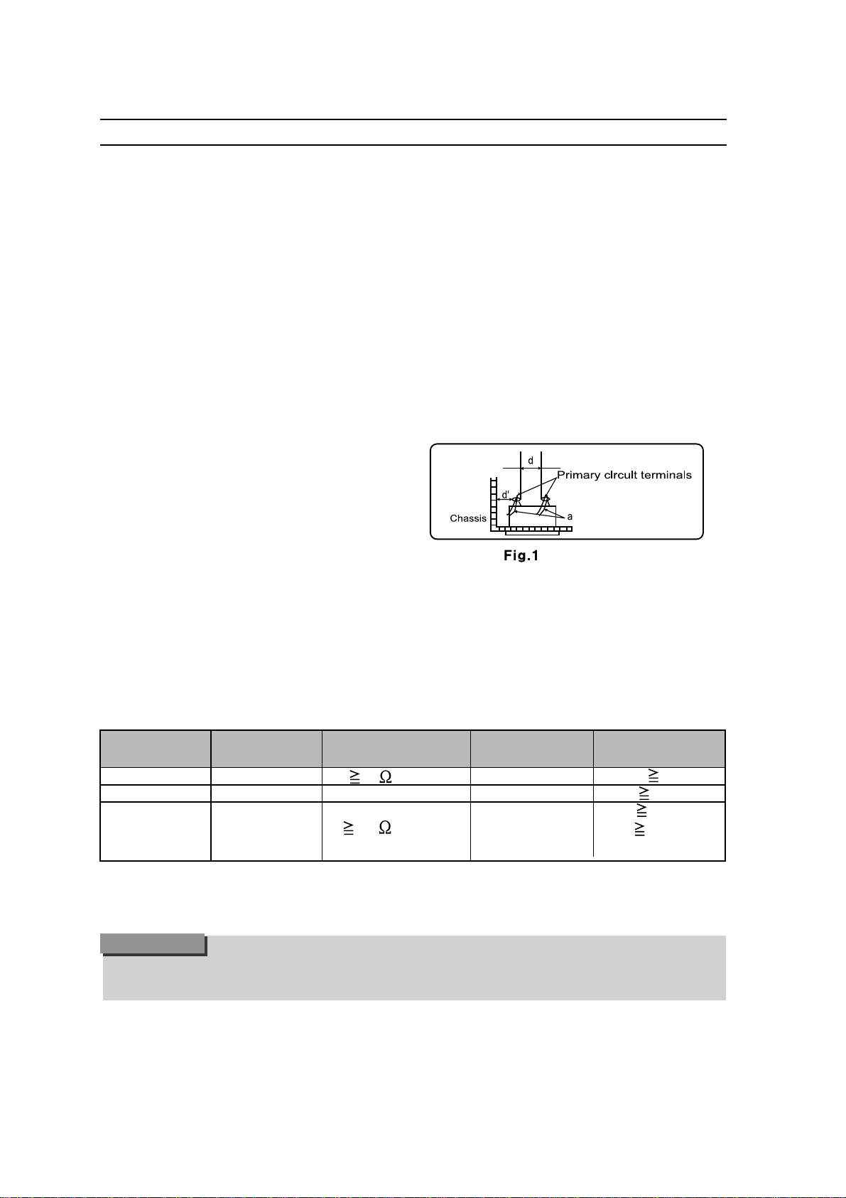
1-3. Clearance distance
When replacing primary circuit component, confirm specified clearance distance (d), (d’) betw een
soldered terminals (see Fig1), and between terminals and surrounding metallic parts. See table 1
below.
Rating for selected areas (table 1)
AC Line Voltage
100V Japan 3
110 to 130V USA &Canada - 900V A C 1min 3.2
110 to 130V
200 to 240V
Class model only
*
Region
Europe 6(d)
Australia 8(d)
Latin America (a : Power cord)
Insulation Dielectric Clearance
Resistance Strength Distance(d),(d’)
1M / 500V DC
10M / 500V DC
1kV AC 1min
4kV AC 1min.
.
NOTE
This table is unoff icial and for reference only. Be sure to confirm the precise values for your particular.
- 2 -
Page 4
Service manual SP-110
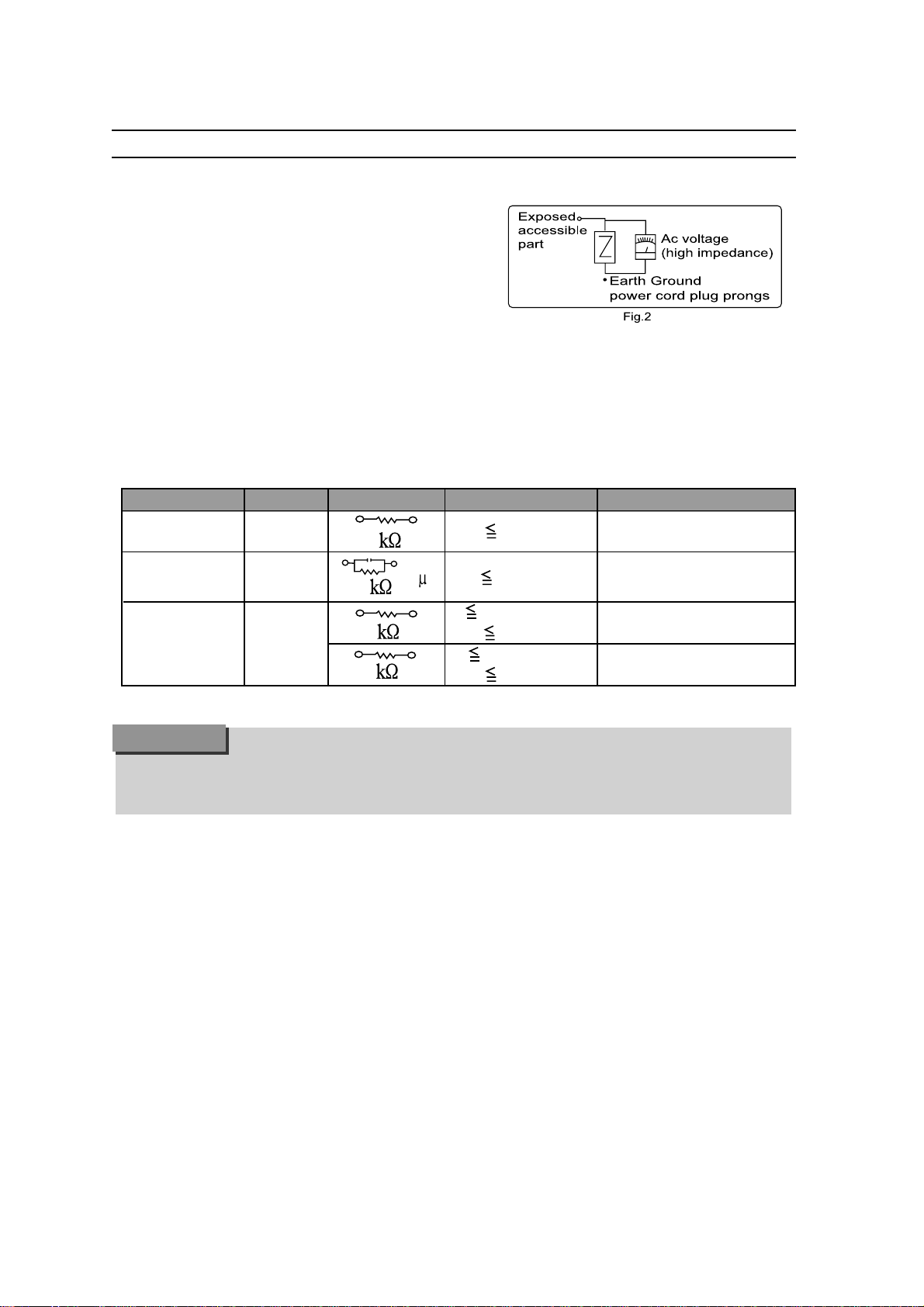
1-4. Leakage current test
Confirm specified or lo wer leakage current between
B(earth ground, power cord plug prongs) and externally
exposed accessible parts (video and audio input terminals, speaker out, etc.)
Measuring method:(Power ON) lnsert load Z between
B(earth ground, power cord plug prongs) and exposed
accessible parts. Use AC voltmeter to measure AC voltage across both terminals of load Z. See Fig.2 and
following table.
Leakage current ratings for selected are as
Ac Line Voltage Region Load Z Leakage Current( i )Clearance Distance(d),(d’)
100V
110 to 130V
110 to 130V
200 to 240V
Japan
USA & Can-
ada
Europe
Australia
1
1
2
50
15 F
i 0.5mArms.
i 0.7mA peak
i 2mAdc
i 0.7mA peak
i 1mAdc
i 1mArms.
Exposed accessible parts
Exposed accessible parts
Antenna earth terminals
NOTE
This table is unofficial and for reference only. Be sure to confirm the precise values
for your particular country and locality.
Other terminals
- 3 -
Page 5
Service manual SP-110
2. PRODUCT SPECIFICATION
[ DSP-4210GM ]
ITEM SPECIFICATION REMARK
1. GENERAL
1-1. MODEL NO DSP-4210GM
1-2. CHASSIS NO SP-110
1-3. SCREEN SIZE 42” (16:9)
1-4. COUNTRY WORLD WIDE
1-5. RESOLUTION 853(W) X 480(H)
1-6. REMOCON TRANSMITTER TYPE R-V2A(ENGLISH), R-V2AK(KOREAN)
1-7. SAFETY STANDARD UL, CSA, CE, KE
2. MECHANICAL
2-1. DIMENSION
1) WITHOUT STAND W X H X D = 1055 X 652 X 85
2) WITH STAND W X H X D = 1055 X 730 X 85
3) BOX W X H X D = 1190 X 870 X 480
2-2. WEIGHT
1) WITHOUT STAND 33kg
2) WITH STAND 39kg
3. ELECTRICAL & OPTICAL
3-1. COMPOSITE VIDEO INPUT SIGNAL NTSC,PAL,SECAM,PAL-M/N,NTSC4.43
1 INPUT ( 75 , 1Vp-p )
3-2. Y/C INPUT SIGNAL 50/60Hz, Super Jack 1 Input( 75 ,1Vp-p )
3-3. DTV/DVD INPUT SIGNAL Y,Pb/Cb,Pr/Cr 1 Input
( 75 ,1Vp-p )
DTV Resolution Mode ( Y, Pb, Pr ) :
*
1920X1080i, 1280X720p,
640X480p
DVD ( Y,Cb,Cr ) : 50/60Hz
*
3-4. PC SIGNAL R,G,B,H,V 15Pin D-sub jack 1 Input
( 75 ,1Vp-p )
* Resolution Mode : VGA - UXGA
3-5. SOUND INPUT SINAL Composite, Y/C : L/R Phone Jack 1Pair
DTV/DVD : L/R Phone Jack 1Pair
PC : L/R Phone Jack 1Pair
Input Impedance 47
*
- 4 -
Page 6
Service manual SP-110
ITEM SPECIFICATION REMARK
3-6. Optical Chracteristics
1) Display Resolution 16:9 Wide 853 X 480
2) Peak Luminance 160cd/ m
3) Contrast Ratio 500:1
4) Color Temperature 8000o K
3-7. Scaling <Scaling Mode>
PC, DTV : Fill to Aspect Ratio,
DVD, VIDEO : Normal, Wide, Panaroma,
Letter Box, Letter Box with Sub Title
<Scaling Adjust>
PC,DTV (User Control) : H-Size, V-Size
3-8. Zoom Zoom
3-9. PIP Video Window in DTV/PC Picture
PIP Size, Position Changeable
3-10.OSD 8Language
KOREAN,ENGLISH,NETHERLAND,
FRENCH,SPANISH,GERMAN,
PORTUGUESE,ITALIAN
3-11. AC Power AC 90V-264V, 50/60Hz
3-12. Power Consumption 350 WATTS
3-13. Sound Output L : 8Watts, R : 8Watts
3-14. LAN Interface Option
3-15. Settop Box Interface Option
3-16. Others Freeze Picture, Video Rotation
2
Fill to Screen
H-Position, V-Position
+
, 4Direction Paning Avaiable
4. USER CONTROL & ACCESSORIES
4-1.CONTROL
1) SET AC POWER, MENU, INPUT SELECT, UP,
DOWN, LEFT, RIGHT
2) REMOCON TRANSMITTER INPUT SELECT,POWER,RECALL, ZOOM-,
ZOOM+,MENU,UP,DOWN,LEFT,RIGHT,
PICTURE MODE,FREEZE,SCREEN MODE,
MUTE
4-2. ACCESSORIES 1) REMOCON : R-V2A, R-V2AK
2) BATTERY : “AAA” 2EA
3) INSTRUCTION MANUA L
4) STAND (OPTION)
5) WALL HANGER (OPTION)
6) SPEAKER UNIT 2ASS’Y (OPTION)
- 5 -
Page 7
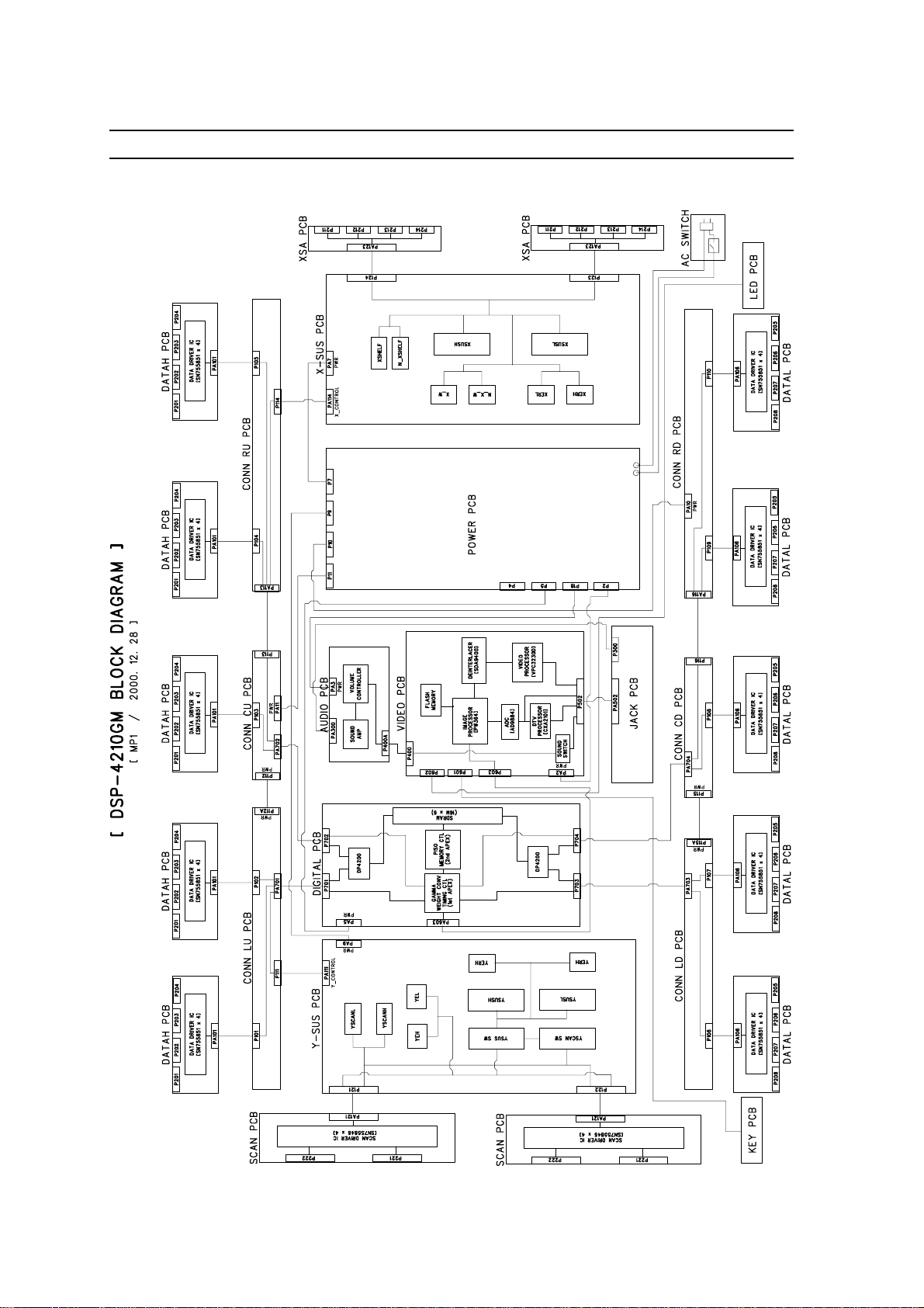
3. BLOCK DIAGRAM
Service manual SP-110
- 6 -
Page 8

4. Adjustment
4-1. How to conf irm the origianl data of VIDEO PCB
(1) Input selection : You select video mode
(2) You confirm the original data of user control
- Brightness : 36 ( :20 in case of DTV/PC input mode )
- Contrast : 60
- Sharpness : 2
- Colour : 32
- T int : 0 ( Center )
(3) You confirm the original data of SERVICE MODE (PW364)
( See 4-4 )
- Sub-Brightness : 60
- Sub-Contrast : 70
- R-Bias : 63
- G-Bias : 63
- B-Bias : 68
- R-Gain : 53
- G-Gain : 57
- B-Gain : 76
Service manual SP-110
4-2. How to adjust POWER PCB
(1) Devices for measurement : Digital volt meter, Pattern generator
(2) Conditions : You adjust as follows after assembling set and inputting WHITE PATTERN.
(Sustain voltage) : Voltage sustaining electronic discharge
1) V
SUS
TP : P12
Adjustment control : RV600
Standard voltage : 166V
2) V
(Scan voltage) : Scan voltage when recording D ATA
SCAN
TP : PA9 #6 PIN of Y PCB
Adjustment control : RV14
Standard voltage : -160V
3) V
(ADDRESS voltage) : Voltage recording DAT A
ADD
TP : P14
Adjustment control : VRS1
Standard voltage : 80V
4-3. X/Y PCB adjustment
(1) Devices for measurement : Digital volt meter, Pattern generator
(2) Previous adjustment voltage : You adjust as follows after assembling set and inputting BLUE
PATTERN.
- 7 -
Page 9

Service manual SP-110
1) V
(SHELF voltage) : X-electrode sustain voltage when recording D ATA
SHELF
TP : RCU25
Adjustment control : RU5
Standard voltage : +60V
(SCAN VH voltage) : VH voltage of SCAN IC when scanning
2) V
VH
TP : RY7 voltage each side
Adjustment control : RY6
Standard voltage : -70V
(3) The final operation adjustment
1) Input a monochrome pattern of R,G,B. And then you check if there are a bnormal OFF-state
pixels (which must be in ON-state but are in OFF-state).
If any, increase V
voltage slowly from 166V to remo v e abnormal OFF state pix els in that
SUS
pattern.
2) If there is no abnormal OFF-state pixel in monochrome pattern of R,G,B, make sure if there is
abnormal OFF-state in Magenta, Cyan, Yellow or not. If any, increase V
slowly in that
SUS
pattern.
3) Increase V
, which is set as above, by 1V.
SUS
4) Make sure if there are abnormal ON-state pixels(which must be on OFF-state but are in ONstate, for example, R or G) in Blue pattern after aging Blue pattern 5 minutes. If any, set V
slowly from - 160V to - 150V and decrease V
slowly to remo v e wrong electronic
SHELF
discharge.
SCAN
4-4. White balance adjustment
(1) Feed grey scale signal to video input terminal.
(2) Confirm the original data of user control (See 4-1).
(3) Press Remote controller in order starting with UP => MUTE => RECALL => MUTE BUTTON
to access Service adjustment mode and select PW364. And then confirm the original data of
the Service mode PW364 register. (See 4-1).
(4) Make sure you can’t recognize an y grey scale errors in the form of colour tint in this darker bands.
(5) You attach the sensor of a White balance meter to the white part on the upper end of this grey
scale pattern.
(6) Set White balance changing R,G,B-Gain.
• You make sure that R,G,B-Gain must be set within the limit of 63 20. If it is over the limit, it
is N.G.
• How to adjust temperature of colour
X = 0.290 0.01, Y = 0.310 0.01
o
Temperature of colour : 8,300
K
(7) You can set Luminance level changing Sub-contrast.
• If the set data of Sub-contrast is over the limit of 80, it is N.G.
(8) Press Menu button, to escape from Service mode.
- 8 -
Page 10

5. When fitting a new board
5-1. V ideo
(1) Check the related adjustments are correctly set as per previous page.
5-2. X-Sustain
Service manual SP-110
(1) Set the V
voltage according to the list of adjustments.
SHELF
(2) The data of adjustment v oltage is on the label, which is attached on the metal part under
Y-Sustain board.
5-3. Y -Sustain
(1) Set the Vvh v oltage according to the list of adjustments.
(2) The data of adjustment voltage is on label, which is attached on the metal part under Y-Sustain
board.
5-4. Power module
(1) You set each voltage according to the list of adjustments.
(2) The data of adjustment v oltage is on the label, which is attached on the metal part under
Y -Sustain board.
- 9 -
Page 11

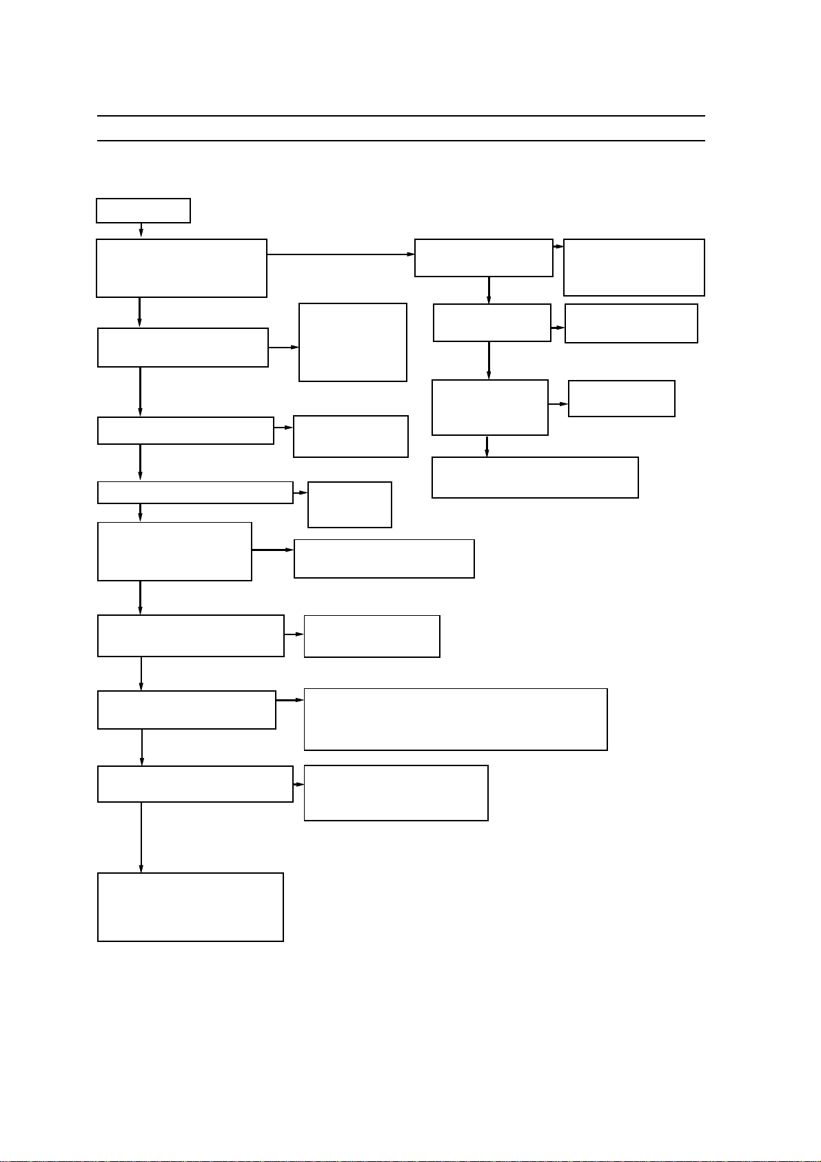
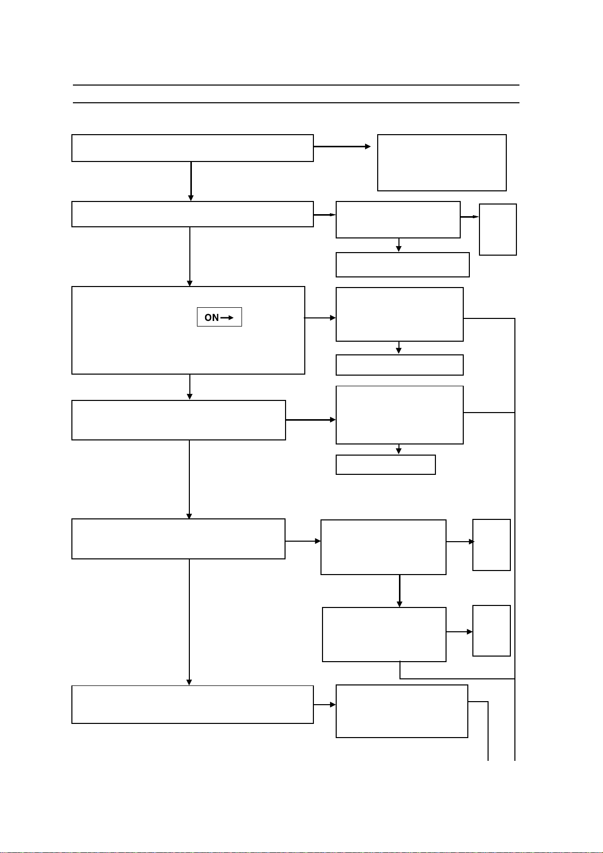
6. Trouble shooting
6-1. Audio/video
6-2. Digital
6-3. X-SUSTAIN
6-4. Y-SUSTAIN
6-5. SCAN Board
6-6. DATA H/L, Connection(LU,CU,RU,LD,CD,RD)
6-7. Power
Service manual SP-110
- 10 -
Page 12
6-1. Audio/V ideo
Service manual SP-110
- 11 -
Page 13
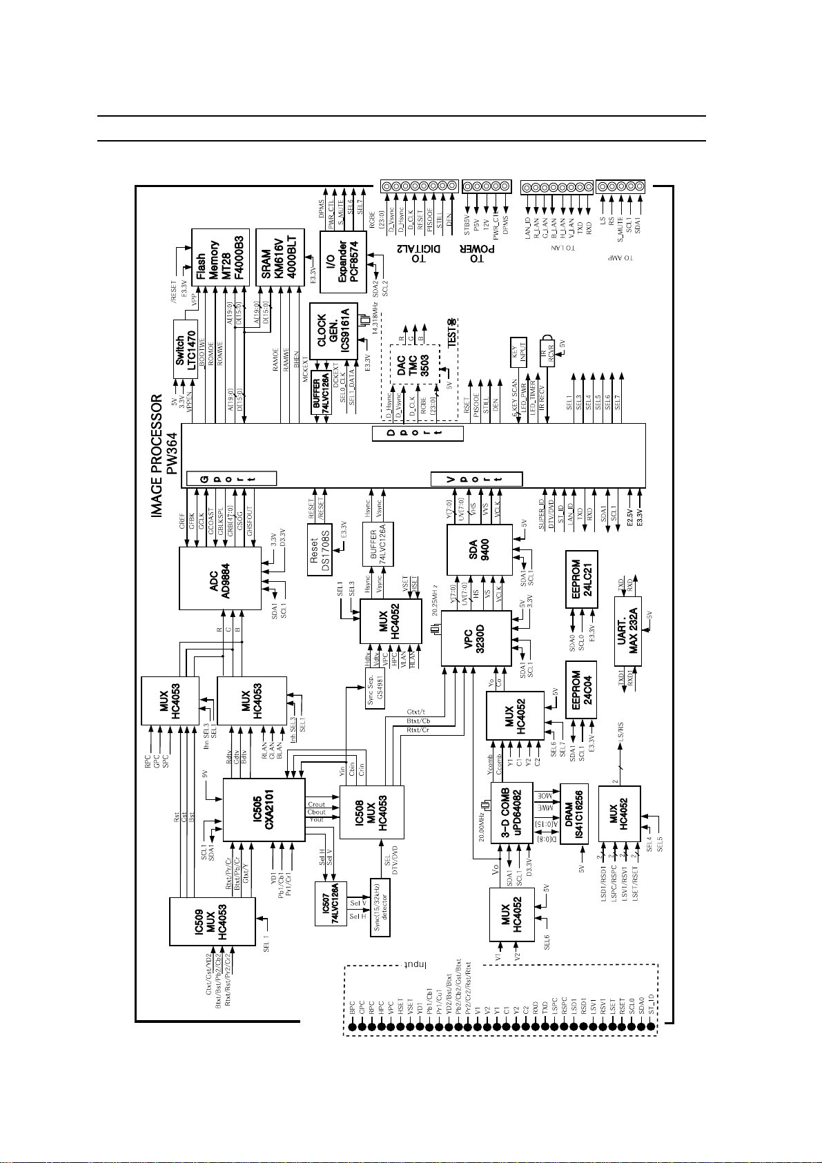
* IMAGE PROCESSOR PART BLOCK DIAGRAM
Service manual SP-110
- 12 -
Page 14
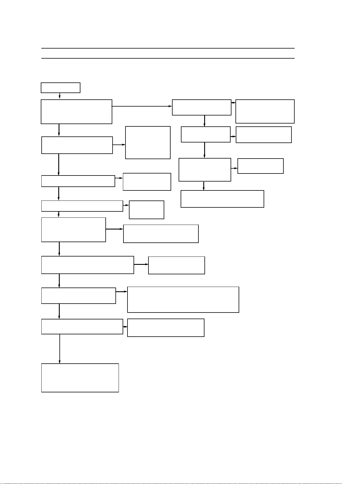
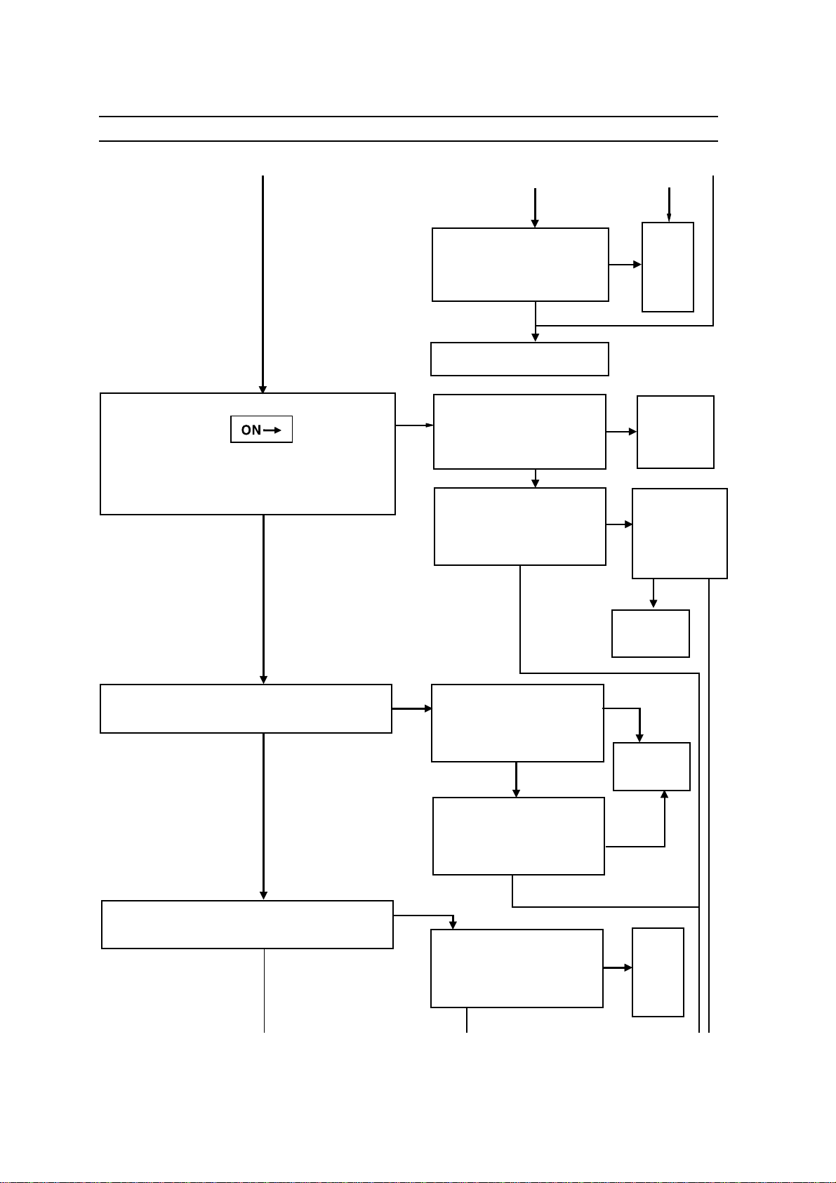
Service manual SP-110
NO Video screen ( Composite input
Check start
Does the ‘Please check input Is there a weak electronic 1.Confirm AC connection
signal or press “input” key.’ discharge on the screen? 2.Confirm Power S/W on
message appear? Y 3.Inspect Digital and X,Y
Y
Is the signal input jack
correctly connected?
Y
Does the input source operate?
Y
Is input selection in Video mode?
Y
Does the ‘DTV, PC’ screen
appear after inputting signal 1. Video signal processing is N.G
to DTV or PC jack? 2. Change video PCB
N
1.Make sure of is PA603 properly Confirm Video to digital
connection of connected? Connector PA603
N
Jack(PDP Monitor
& A/V de vice)
is DVS,DHS,DCLK Video PCB is N.G
of Video PCB P603 Change PCB
N
Operate A/V device, being outputted?
Which is used.
N
Confirm
input selection
)
NN
N
Y
N
Y
1.Confirm other PCBs Video PCB than
2.Change PA603
Y
Can you see input to P502 No.43 V1 1. Inspect jack PCB
of Video PCB? 2. Inspect input jack
Y
Can you see input to TP Y0, V0? 1. Video S/W and 3D COMB filter
(IC402) are N.G
2. Change video PCB
Can you output Sync of TP V2 : 60Hz/ 1. Confirm if IC400 and IC401
50Hz H2 : 31.5KHz/KHz? are N.G
2. Change video PCB
1. Video signal processing is N.G
2. Change Video PCB
Y
Y
N
N
N
CAUTION : 1.You must only remove PA603 after confirming
that you switch off the power.
2. You must thoroughly understand instruction manual
before removing Back cover.
- 13 -
Page 15
Service manual SP-110
NO DTV screen (1080I, 720P, 480P)
Check start
NN
Does the ‘Please check input Is there a weak electronic 1.Confirm A C connection
signal or press “input” key.’ discharge on the screen? 2.Confirm Power S/W on
message appear? Y 3.Inspect Digital and X,Y
Y
Is the signal input jack
correctly connected?
Y
Does the input source operate?
Y
Is input selection in DTV/DVD mode?
Y
Does the ‘V ideo’ screen
appear after inputting signal 1. DTV signal processing is N.G
to Video jack? 2. Change video PCB
N
1.Make sure of is PA603 properly Confirm Video to digital
connection of connected? Connector PA603
N
Jack(PDP Monitor
& A/V de vice)
is DVS,DHS,DCLK Video PCB is N.G
of Video PCB P603 Change PCB
N
Operate A/V device, being output?
Which is used.
N
Confirm
input selection
1.Confirm other PCBs than Video PCBs
2.Change PA603
Y
Y
N
N
Y
Can you see input to P502 No.10 1. Inspect jack PCB
YD1 of Video jack? 2. Inspect input jack
Y
Can you output DTV signal in 1. DTV S/W and DTV processor(IC505) circuit are N.G
TP R,G,B? 2. DTV H/V Sync processing part is N.G
3. Change video PCB
Can you output Sync of TP V1:Hz/ 1. DTV S/W and DTV processor
H1 : KHz/ Hz? (IC505) circiuit are N.G
2. Change video PCB
1. Video signal processing is N.G
2. AD Converter(IC500) is N.G
3. Change Video PCB
Y
Y
N
N
N
- 14 -
Page 16
Service manual SP-110
NO PC screen
Check start
NN
Does the ‘Please check input Is there a weak electronic 1.Confirm AC connection
signal or press “input” key.’ discharge on the screen? 2.Confirm Power S/W on
message appear? Y 3.Inspect Digital and X,Y
Y
Is the signal input jack
correctly connected?
Y
Does the input source operate?
Y
Is input selection in PC mode?
Y
Does the ‘V ideo’ screen
appear after inputting signal 1. PC signal processing is N.G
to Video jack? 2. Change video PCB
Y
Can you see input to P502 No.9,8,31,32,33 1. Inspect jack PCB
R,G,B,Hsync,Vsync of Video PCB? 2. Inspect input jack
Y
Can you output PC signal in 1. PC S/W and DTV processor(IC505) are N.G
TP R,G,B? 2. PC H/V Sync processing part is N.G
3. Change video PCB
Can you output Sync of TP V1 : Hz/ 1. PC S/W is N.G
H1 : KHz/ Hz? 2.Change video PCB
Y
N
1.Make sure of is PA603 properly Confirm Video to digital
connection of connected? Connector PA603
N
Jack(PDP Monitor
& PC)
Does DVS,DHS,DCLK Video PCB is N.G
of Video PCB P603 Change PCB
N
Operate A/V device, being output?
Which is used.
N
Confirm
input selection
N
N
N
1.Confirm other PCBs than Video PCB
2.Change PA603
Y
Y
N
N
Y
1. PC signal processing is N.G
2. A/D Converter is N.G
3. Change Video PCB
- 15 -
Page 17
NO Sound
Check start
Service manual SP-110
Does the screen appear?
Y
is the sound signal input jack
correctly connected?
Y
is the speaker properly connected?
Y
Is sound signal output from P502?
Y
is sound signal on P400 No.2,3
of audio PCB?
Y
is sound signal on PA400 No.2,4 1. PA400 connector is N.G
of audio PCB? 2. Change audio PCB
N
N
1. Confirm AC connection
2. Confirm po wer S/W on
3. Inspect video PCB and other blocks
N
1.Make sure of connection of jack(PDP monitor & A/V device)
N
Connect speaker
N
1. Jack PCB is N.G
2. Video connection to
jack PCB is N.G
1. Sound S/W is N.G
2. Confirm IC404
3. Change video PCB
N
See: Siganl composition of P502 sound
1. RSPC, LSPC => PC sound
2. RSD1, LSD1 => DTV/DVD sound
3. RSV1, LSV1 => VIDEO, S-VHS sound
Y
is sound AMP on PA300 No.1,4 of Is power fed to PA3 of 1. Confirm if PA3 connector is N.G
audio PCB processing an output? audio PCB? 2. Change power board
Y
Does sound AMP on PA300 No.1,4 and
JP659 of audio PCB produce an output?
Y
1. Speaker or sound cable is N.G
2. Change speaker or sound cable
N N
Y
N
1. PA300 is N.G (Change audio PCB)
or JP659 is N.G (Change jack PCB)
- 16 -
Page 18
NO Remote Controller operation
Check start
N
Is red LED next to PO WER S/W
on?
Y
Service manual SP-110
1. Confirm AC connection
2. Confirm po wer S/W on
3. Inspect video PCB, LED PCB and other
blocks
Does Remote Controller operate?
Y
Is screen on with key input?
Y
Is there waveform when pressing remocon
in IR NO.2 of P602
1. IR receipt block of video PCB is N.G
2. Inspect video PCB and other PCBs
N
1. Confirm Remote Controller operation and battery
N
1. Connection with video PCB is N.G or video PCB N.G
2. Inspect video PCB and other blocks
N
1. LED PCB is N.G
2. Change LED PCB
- 17 -
Page 19
NO Key operation
Check start
Is red LED on next to POWER S/W
on?
Y
N
1. Confirm AC connection
2. Confirm po wer S/W on
3. Inspect video PCB, LED PCB and other
blocks
Service manual SP-110
Does power come on with
remocon?
Y
Is connection between PA601 of key PCB
and video PCB good?
Y
1. Inspect video PCB and other PCBs
N
1. Connection with video PCB is N.G or
V ideo PCB is N.G
2. Inspect video PCB and other blocks
N
1. PA601 connector is N.G
2. Change key PCB
- 18 -
Page 20

Service manual SP-110
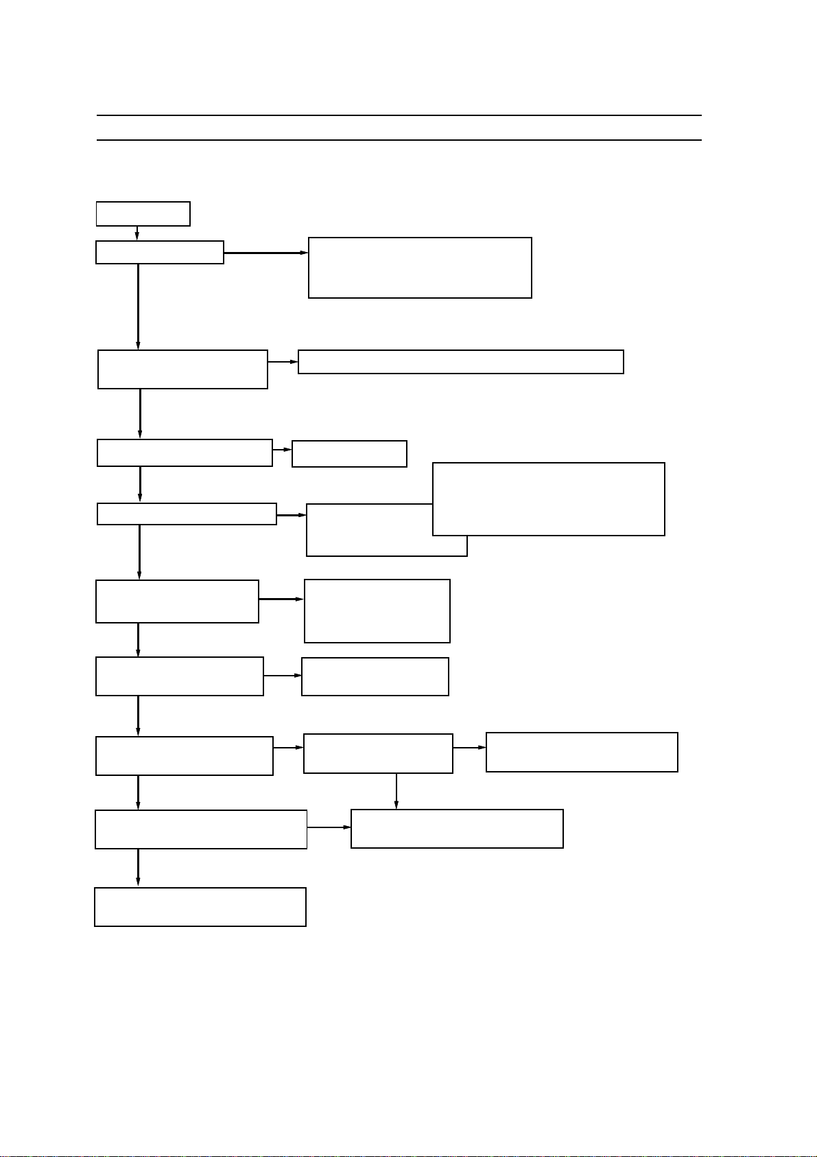
6-2. DIGITAL
Checking Order for normal operation of Digital Board and Check Points
( * Measure RMS voltage with a multi-meter , refer to the attached picture for position of
check points )
1. After make sure that the set turns off, turn off the High Voltage ON/OFF Switch of the Power
Board and then turn on the set
2. Confirm whether there is an input of 5V, 3.3V into Power Connector ( PA5 ).
- 5V input (pin No.1,2) : If 4.5V ~ 5.2V, O.K.
- 3.3V input (pin No.7,8) : If 3.0V ~ 3.5V, O.K.
3. Confirm whether Power 2.5V, 3.3V_1, 3.3V_2, 3V_3, 5V_1, 5V_2
- 2.5V : If 2.2V ~ 2.7V, O.K.
- 3.3V : If 3.0V ~ 3.5V, O.K.
- 5V : If 4.5V ~ 5.2V, O,K.
4. Confirm Reset and V_MUTE
- Reset : If 3.0V ~ 3.5V, O.K.
- V_MUTE :If 3.0V ~ 3.5V, O .K.
5. Confirm CONF_DONE ( ID102, ID103 )
- CONF_DONE : If 3.0V ~ 3.5V, O.K.
- 19 -
Page 21
Service manual SP-110
- 20 -
Page 22
Service manual SP-110
6-3. X-SUSTAIN BOARD
1. Separate PA7 and PA114 connector
2. Check the remaining electrical voltage of PA7
(1) Check the Voltage of Terminal 170V : If maintained beyond 10 volt, discharge (belo w 5 v olt)
with resistance of beyond 1K ohm 5 Watt
3. Confirm the v alue of series and parallel resistance of RU10//RU13-R U11//RU14-RU12//R U15
(1) Each value of resistance : 6.8 ohm 5 Watt
(2) The total value of resistance : 10.2 +/- 0.5 ohm
(3) In case of wrong value of resistance, replace (open) board and conf irm each connector
: the state of insertion ( installation )
4. In case of normal value of resistance, measure the v alue as follo wing table1.
(1) Use a Diode Tester
(2) If abnormal part is found, replace the board
(3) In case of normal state, Inspect connectors and other boards
Table 1. P A7 The value of Diode Tester of each terminal
+ : red, - : black
*
NAME DIODE MEASURE DIODE MEASURE
TESTER TESTER
1 170V + About 5 sec. - 0.49
GND - Later, +
Open
2 15V + About 3 sec. - 0.47
GND - Later, +
Open beyond 2V
3 CU1(5V) + Beyond 1.43 - 0.48
GND - +
Table 2. PA114 The v alue of Diode Tester of each terminal
+ : red, - : black
*
The configuration of terminal ( top view, components side )
- 21 -
Page 23
Service manual SP-110
DIODE TESTER MEASURE DIODE TESTER MEASURE
- + + -
GND A 0.6 GND A 0.5
B 0.6 B 0.5
C 0.6 C 0.5
D 0.6 D 0.5
E 0.6 E 0.5
F 0.6 F 0.5
G 0.6 G 0.5
H 0.6 H 0.5
Table 3. The value of Diode Tester of each Semiconductor
+ : red, - : black
*
NAME DIODE MEASURE DIODE MEASURE
TESTER TESTER
1 QU5/QU6 D + ABOUT 5 - 0.48
S - SEC. LATER, +
OPEN
2 QU7/QU8 D + Open - 0.48
S- +
3 QU17/QU18 D + Open - 0.45
S- +
4 QU15/QU16 D + Open - 0.45
S - +
5 QU23~QU26 D + Open - 0.4
S- +
6 QU19~QU22 D + Open - 0.4
S- +
7 QU12 D + Open - 0.49
S- +
8 QU11 D + Beyond 2.3 - 0.49
S- +
9 QU9 D + ABOUT 5 - 0.5
S - SEC.LATER, +
OPEN
10 QU4 D + Open - 0.5
S- +
11 QU13/QU14 D + Open - 0.48
S- +
- 22 -
Page 24
Service manual SP-110
6-3. Y -SUST AIN BOARD
1. Separate PA9, PA111 connector
2. Confirm the remaining electrical Voltage of PA9
(1) Confirm the Voltage of T erminal 170V : If maintained be yond 10 v olt, dischar ge(below 5 volt)
with resistance of beyond 1K ohm 5 Watt
(2) Confirm the Voltage of T erminal -155V : If maintained be yond -10 v olt, dischar ge(belo w -5
volt) with resistance of beyond 1K ohm 5Watt
3. Confirm the resistance of RY2 ( 470 ohm 5W att )
(1) In case of wrong value, replace board and conf irm each connector
4. In case of normal value of resistance, measure the value as following Table 1.
(1) Use a Diode Tester
(2) If abnormal part is found, replace the board
(3) In case of normal state, Inspect connectors and other boards
Table 1. PA9 The value of Diode Tester of each terminal
+ : red, - : black
*
NAME DIODE MEASURE DIODE MEASURE
TESTER TESTER
1 170V + About 3 Sec. Later, - Beyond 0.8
GND - Open +
2 -155V + Beyond 0.7 - Open
GND - +
3 ON/OFF + Open - Beyond 2.4
GND - +
4 15V + Beyon 0.7 - About 5 Sec. Later, beyond 0.4
GND - +
Table 2. PA111 The v alue of Diode Tester of each terminal
+ : red, -: black
*
The configuration of terminal (top view, components side)
- 23 -
Page 25
Service manual SP-110
DIODE TESTER MEASURE DIODE TESTER MEASURE
- + + -
GND A 1.2 GND A 0.5
B 0.6 B 0.5
C 0.6 C 0.5
D 0.6 D 0.5
E 1.2 E 0.5
F 1.2 F 0.5
G 0.6 G 0.5
H 0.6 H 0.5
I 0.6 I 0.5
J 0.6 J 0.5
K 1.2 K 0.5
L 0.6 L 0.5
M 0.6 M 0.5
P 1.2 P 0.5
Table 3. The value of Diode Tester of each Semiconductor
+ : red, - : black
*
NAME DIODE MEASURE DIODE MEASURE
TEST TEST
1 QY5~QY8 D + ABOUT 3 - 0.4
S - SEC. LATER, +
OPEN
2 QY9~QY12 D + Open - 0.4
S- +
3 QY1~QY2 D + Open - 0.4
S- +
4 QY3~QY4 D + Open - 0.4
S- +
5 QY25~QY28 D + Open - 0.4
S- +
6 QY20~QY23 D + Open - 0.4
S- +
7 QY15~QY16 D + Open - 0.4
S- +
8 QY19 D + Open - 0.4
S- +
9 QY14 D + Open - 0.4
S- +
10 QY13 D + Beyond 1 - Open
S- +
11 QY2 D + Open - 0.4
S- +
- 24 -
Page 26
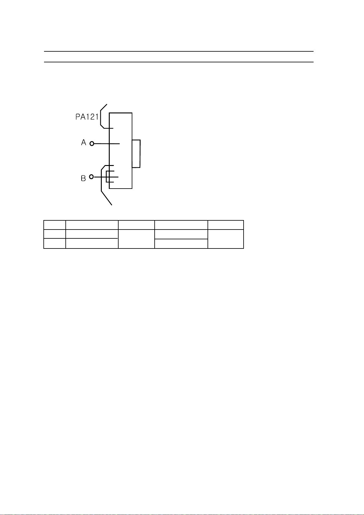
6-5. SCAN BOARD
1. Confirm the DIOED TESTER, PCB separately
2. The configuration
(1) The Voltage Terminal of Scan (top view, components side)
DIODE TESTER MEASURE DIODE TESTER MEASURE
A + Beyond 0.6 - Open
B- +
Service manual SP-110
- 25 -
Page 27
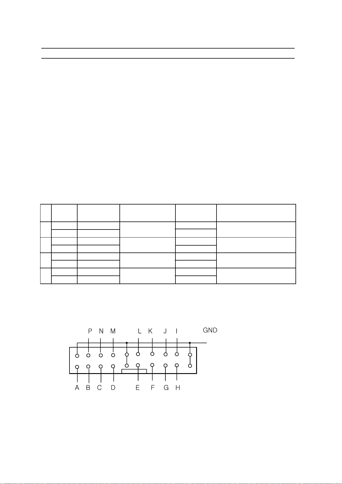
6-6. D ATA H/L, CONNECTION(RU,CU,LU,RD,CD,LD)
1. Confirm the upper part and the lo wer part
(1) Separate PA10 and PA11
(2) Confirm DIODE TESTER
2. Separate P112
(1) Confirm LU and two DATA H boards
3. Separate PA113
(1) Confirm CU and DATA H board
(2) Confirm RU and two DATA H boards
4. Separate P115
(1) Confirm LD and two DATA L boards
5. Separate P116
(1) Confirm CD and DATA L board
(2) Confirm RD and two DATA L boards
Table 1. The value of Diode Tester of each terminal
+ : red, - : black
*
NAME DIODE TESTER MEASURE DIODE TESTER MEASURE
1 Vadd + Open - 0.6
GND - +
2 5V + Beyond - 0.5
GND - 1.3 +
Service manual SP-110
- 26 -
Page 28
Service manual SP-110
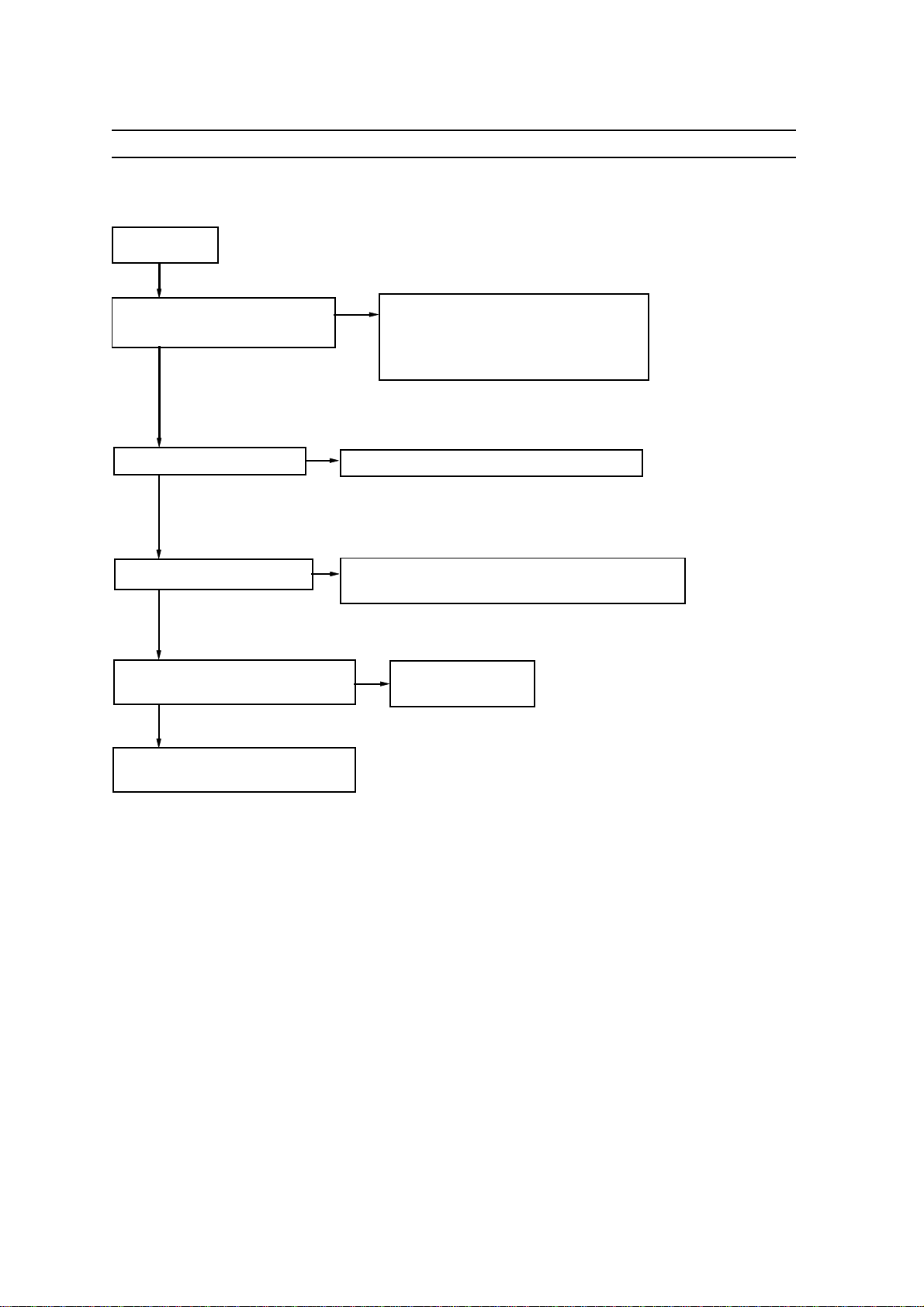
6-7. POWER CHECK
NO
When the set is switched on, the power LED turns red? 1. Check Fuse F1 open
2. Check RC 1(Bridge Diode)
YES
open/short
NO
NO
When remote controller is switched on, LED turns green? Is 7PIN of CONNECTOR P2 Check
0 V? VIDEO
PCB?
YES
Check R20, R21, R22 open
Push the SW1 (Slide switch) of POWER MODULE After P3 CONNECTOR is
NO
NO
in the opposite direction of separated, is each voltage
Then, check LOW B+. (30V, 12V, 5V) correct?
Is each voltage (30V, 12V, 5V) of CONNECTOR P3
YES
correct? Check Audio AMP PCB
YES
After P5 CONNECTOR is
Is each voltage(5V, 3.3V) of CONNECTOR P5 separated, is each voltage
NO
NO
correct? (5V, 3.3V) correct?
YES
Check Digital PCB
YES
Is 1 pin voltage of CONNECTOR P7 and P9
correct at 15V?
YES
Is 1 pin voltage of CONNECTOR P10 and P11 correct
at 15V?
NO
- 27 -
After P7 CONNCETOR is
Separated, 15V
present?
NO
After P9 CONNCETOR is
Separated, 15V
present?
NO
NO
After P10 CONNCETOR is
Separated, 15V
present?
YES
YES
Check
X-sus
PCB
Check
Y-sus
PCB
YES
Page 29
Service manual SP-110
YES
Push the SW1(Slide Switch) POWER Module
in the direction of
Then, check High Voltage
And turn on the Power,
Can Vsus(170V) be produced?
YES
After P11 CONNECTOR is
Separated, is 15V
produced?
Replace Power Module
Without Connector P7
NO
Can Vsus(170V) be
producde?
Without Connector P9
Can Vsus(170V) be
produced?
NO
NO
NO
Check
YES
CONNECTION
PCB
Check
YES
X-sus PCB
Is the
YES
Vol ta ge
Of Conncetor
P7,5PIN 0V?
Check
Y-sus PCB
YES
YES
NO
Turn on the POWER. Can Vadd(70V) be
produced?
YES
Turn on the POWER. Can Vscan(-155V) be
produced?
YES
NO
NO
- 28 -
Without Connector P10
Can Vadd(70V) be
produced?
NO
Without Connector P11
Can Vadd(70V) be
produced?
NO
Without Connector P9
Can Vscan(-155V) be
produced?
YES
Check
Y-sus PCB
YES
Check
YES
Y-sus
PCB
Page 30
E N D
Service manual SP-110
NO
Replace
POWER
Module
- 29 -
Page 31

7. Assembly List
NO
PCB ASS’Y NAME
WORKING PR OCESS ASSEMBLY
ASS’Y NAME CODE
1 A CCESSOR Y AS PEACPWD011
2 PACKING AS PEPKCPD011
3 CABINET AS PECACAD011
4 MASK FRONT AS PEFMSJD011
5 VIDEO PCB AS
6 PCB VIDEO MANUAL A PEVDMSD011
7 PCB VIDEO CHIP B AS PEVDJ2D011
8 PCB VIDEO CHIP A AS PEVDJ1D011
9 DIGITAL PCB AS
10 PCB DIGITAL MANUAL PEDGMSD011
11 PCB DIITAL CHIP B PEDGJ2D011
12 PCB DIGIT AL CHIP A A PEDGJ1D011
13 DATA_H PCB AS PCB DATA H AS PED1MSD011
14 PCB DATA H CHIP A A PED1J1D011
15 DATA_L PCB AS
16 PCB DATA L MANUAL PED2MSD011
17 PCB DATA L CHIP A A PED2J1D011
18 SCAN PCB AS
19 PCB SCAN MANUAL A PES1MSD011
20 PCB SCAN CHIP A AS PES1J1D011
21 X-SUS PCB AS
22 PCB X-SUS MANUAL A PEXSMSD011
23 PCB X-SUS RHU AS PEXSJ0D011
24 PCB X-SUS M-10 AS PEXSJBD011
25 PCB X-SUS RADIAL AS PEXSJRD011
26 PCB X-SUS CHIP A AS PEXSJ1D011
27 Y-SUS PCB AS
28 PCB Y -SUS MANUAL A PEYSMSD011
29 PCB Y -SUS RHU AS PEYSJ0D011
30 PCB Y -SUS M-10 AS PEYSJBD011
31 PCB Y -SUS RADIAL AS PEYSJRD011
32 PCB Y-SUS CHIP A AS PEYSJ1D011
33 AUDIO PCB AS
34 PCB AUDIO MANU AL A PEAUMSD011
35 PCB AUDIO RADIAL AS PEA UJRD011
36 PCB AUDIO AXIAL AS PEA UJ AD011
37 JACK PCB AS
38 PCB JACK MANUAL AS PEJAMSD011
39 XSA PCB AS
40 PCB XSA MANUAL AS PEXAMSD011
41 CONN UNION
42 PCB AS PCB UNION CHIP A AS PEUNJ1D011
43 PCB UNION AS PEUNSWD011
44 PCB RIGHT-DO MANU PERWMSD011
45 PCB RIGHT-DO A AS PERWJ1D011
- 30 -
Service manual SP-110
Page 32

8. Block Diagram
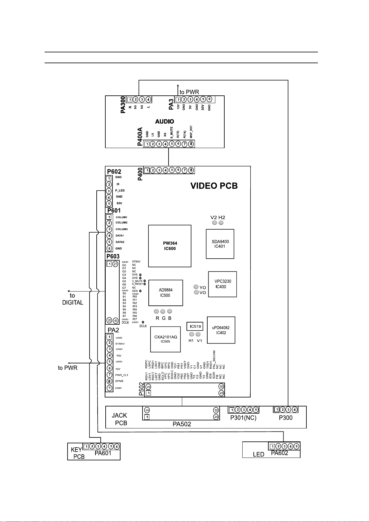
8-1. VIDEO / A UDIO
Service manual SP-110
- 31 -
Page 33

8-2. Digital
Service manual SP-110
- 32 -
Page 34

8-3. Y -Sustain
Y-Sustain Block Diagram
Service manual SP-110
- 33 -
Page 35

8-4. X-Sustain
·
·
·
·
·
·
X-Sustain Block Diagram
Service manual SP-110
- 34 -
Page 36

Page 37

686, AHYEON-DONG MAPO-GU
SEOUL, KOREA
C.P.O. BOX 8003 SEOUL, KOREA
TELEX : DWELEC K28177-8
CABLE : “DAEWOOELEC”
E-mail :djkoo@web.dwe.co.kr
TEL : 82-2-360-7806
FAX : 82-2-360-7877
Page 38

Page 39

Page 40

Page 41

Page 42

Page 43

Page 44

DSP-4210GM
Data-board change procedure
Daewoo Electronics
Page 45

Step 1.
Un-screw the following locations.
This is backside of PDP. The circled locations are where the screws in
order to take off the back panel.
Page 46

Step 2
Inside look of PDP
This is inside look of PDP. The upper data board is different from bottom.
Upper: “Data High”, Lower: “Data Low”. You can read these on the board.
Page 47

Step 3
Page 48

Step 4
Testing. Find out the exact location of the line by pictures.
Connect any video source and display. This is normal picture.
Page 49

Step 5
Testing. Unhook the data connector.
Find out exact location of the line and unhook the connector right above
that position.
Page 50

Step 6
Picture of opened hook.
Page 51

Step 7
Take out the connect strip.
Page 52

Step 8
Exam the picture.
You will see some thin dead lines vertically.
Page 53

Step 9
Close look of the picture
If you still see the problem line in between these dead lines, then you have
to change the “Data Low (Lower)” board.
If you cannot see the problem line between these dead lines, you have to
change the “Data High (Upper)” board.
Page 54

Step 10
Changing Data High. Unhook all the connectors.
Page 55

Step 11
Unscrew
Page 56

Step 12
Pull the data board and replace with new one.
Page 57

Step 13
Slide in the new board
Page 58

Page 59

Step 14
1. Push in the connector
2. Push down the clip.
**** Caution ****
At the tip of the connector, there is a little hook. So lift a little and push in
all the way, and then clip down.
Page 60

Step 15
Screw in.
Step 16
Same technic is applied if you have to change the “Data Low
(Lower)”
Page 61

Page 62

Step 17
Put back the back cover.
Page 63

Please send back the Defected parts to the following address.
Daewoo Electronics DTV Service.
120 Chubb Ave.
Lyndhurst, NJ 07071
If you have any question?
Call 1-800-Daewoo-8 (1-800- 323-9668) or,
Email: service@daewoodigital.com
Page 64

DSP-4210GM
Horizontal Data-board change procedure
Daewoo Electronics
Page 65

Step 1.
Un-screw the following locations.
This is backside of PDP. The circled locations are where the screws in
order to take off the back panel.
Page 66

Step 2
Inside look of PDP
Page 67

Step 3
Horizontal Data board (Showing bottom one for example)
Page 68

Step 4
Pull out the 2 connectors.
Page 69

Step 5
Unscrew 2 positions
Page 70

Step 6
Slide and disconnect the board from main unit.
Page 71

Step 7
Slide in the new board.
Page 72

Step 8
Screw in the 2 screws in the position
Page 73

Step 9
Put in the data connector.
Page 74

Step 10
Cover the back panel and screw in those positions.
Page 75

Step 11
Please send back to us the unused and defected part.
Please mark which one is unused and defected.
Address:
Daewoo Electronics Research Center
120 Chubb Ave.
Lyndhurst, NJ 07071
Phone Number
201-964-9349
Page 76

DSP-4210GM
Data board change procedure
(When multiple thin lines occur in-group)
Daewoo Electronics
Page 77

Step 1.
Un-screw the following locations.
This is backside of PDP. The circled locations are where the screws in
order to take off the back panel.
Page 78

Step 2
Look for the position of the lines occur.
Close Look
Page 79

If the lines occur in the middle of screen, disassemble the connecter part.
Step 3.
Unscrew those positions.
Page 80

Step 4
Take out the wires and the connector.
Page 81

Step 5.
Slide out the input connector consol.
** Note **
Input connecting consol is still connected with power cable. Therefore, Do
not pull the consol to get completely separate from the main unit.
Page 82

Step 6.
Picture after input connecting consol is detached.
Page 83

Step 7.
Check if any connection is loosed.
Close Look
Page 84

If there is no connector that is loosed, change data-board.
Step 7.
Change Data-board.
See Data-board Change procedure.
Step 8.
Changing Data-board controller. (Step 8 ~ Step ??)
Location of Data-board Controller
Page 85

Page 86

How To Access Service Mode for Screen Control
1. Turn on the PDP.
2. Set up the PDP and a picture source. E.g. PDP and DVD are connected with component or
composite connection.
3. Play any DVD and select a picture scene and pause it. When you select a picture scene, try to
find a scene has bright (light source) spot and dark (shadow) spot in the same picture. (e.g. A
little dark room with bright light comes through a window.)
4. Go into the “service menu” mode using your remote control.
(Press following order on your remote: Up -> Mute -> Recall -> Mute)
5. You will see the Following option on the center of the screen.
CXA2101AQ
VPC3230D
PW364
MSP3405P
PICTURE
Test Pattern
Factory
6. Highlight the option “PW364” by pressing “down” arrow.
7. Select the option by pressing “right” arrow.
8. You will see the following option.
S Brt
S Cont
R Bias
G Bias
B Bias
R Gain
G Gain
B Gain
9. “S Brt” is the Brightness and “S Cont ” is the Contras.
10. Write down all the values on that screen and use this as a reference.
11. Highlight S Brt.
12. Change its value to “0” by press left arrow.
13. Highlight S Cont.
14. Change its value to “0” by press left arrow. (You will see almost nothing)
Page 87

15. Increase “S Cont ” value using “Right” arrow until you see the bright spot of the picture.
You still don’t see the dark (shadow) spot of the screen but it is ok.
16. Highlight “S Brt” by pressing “up” arrow once.
17. Increase its value using “right” arrow until you see the dark (shadow) spot of the screen.
18. Exit the service menu by pressing “Exit” button twice.
19. Turn off the PDP and Turn on again.
20. Enjoy your PDP.
Page 88

INSTRUCTION MANUAL
DSP-4210GM
Page 89

Important safety instructions
FCC regulations state that any
unauthorized changes or
modifications to this equipment many
void the user's authority to operate it.
To prevent electric shock, use a 3-wire
grounding-type plug, and fully insert
the plug.
To prevent damage which may result in fire or
electric shock hazard, do not expose this
appliance to rain or moisture.
Important safety information
Always be careful when using your monitor. To
reduce the risk of fire, electrical shock, and
other injuries, keep these safety precautions in
mind when installing, using, and maintaining
your machine.
Read all safety and operating instructions
before operating the PDP monitor.
Retain the safety and operating instructions
for future reference.
Heed all warnings on the monitor and in the
operating instructions.
Follow all operating and use instructions.
Unplug this monitor from the wall outlet
before cleaning. Use a damp cloth; do not
use liquid or aerosol cleaners.
Never add any attachments and/or equipment
without approval of the manufacturer. Such
additions may result in the risk of fire,
electric shock, or other personal injury.
Do not use the monitor where contact with or
immersion in water is a possibility, such
as near bath tubs, sinks, washing machines,
swimming pool, etc.
Provided ventilation for the monitor. The
unit is designed with slots in the cabinet for
ventilation to protect it from overheating. Do
not block these openings with any object. On
not place it near a radiator or heat register.
Operate your monitor only from the type of
power source indicated the marking label. If
you are sure of the type of power supplied to
your home, consult your monitor dealer or
local power company.
This plug will fit into a grounding-type
power outlet only one way. If you are unable
to insert the plug into the outlet, contact your
electrician to replace your outlet. Do not
defeat the purpose of the grounding-type
plug.
This monitor is equipped with a 3-wire
grounding-type plug. That is, a plug having a
third (grounding) pin.
Protect the power cord. Power supply cords
should be routed so that they are unlikely to
be walked on or pinched by items placed on
or against them. Pay particular attention to
cords at plugs, convenience receptacles, and
the point where they exit from the unit.
CAUTION
TO REDUCE THE RISK OF
ELECTRIC SHOCK, DO NOT
REMOVE COVER ( OR BACK )
NO USER SERVICEABLE PART INSIDE REFER
SERVICING TO QUALIFIED SERVICE PERSONNEL
Page 90

Unplug the monitor from the wall outlet and
disconnect the interfacing cable system
during a lightning storm or when left
unattended and unused for long periods of
time. This will prevent damage to the unit
due to lightning and power-line surges.
Avoid overhead power lines. An external
connection cables should not be placed in the
vicinity of overhead power lines or other
electric light or power circuits. When
installing an external connection cables be
careful to keep from touching the power
lines or circuits. Contact with such lines can
be fatal.
Do not overhead the wall outlet or extension
cords. Overloading can result in fire or
electric shock.
Do not insert foreign objects through
openings in the units, as they may tough
dangerous voltage points or damage parts.
Never spill liquid of any kind on the monitor.
Do not attempt to service this monitor
yourself. Refer all servicing to qualified
service personnel. Unplug the unit from the
wall outlet and refer servicing to qualified
service personnel under the following
conditions :
when the power-supply cord or plug is
damaged
if liquid has been spilled on or objects
have fallen into the unit
if the monitor has been exposed to rain or
water
if the monitor does not operate normally
by following the operating instructions
if the monitor has been dropped or the
cabinet has been damaged
when the monitor exhibits a distinct
change in performance
If you make adjustments yourself, adjust
only those controls that are covered by the
operating instructions. Adjusting other
controls may result in damage and will often
require extensive work by a qualified
technician to restore the monitor to normal.
When replacement parts are required, be sure
the service technician uses replacement parts
specified by the manufacturer or those that
have the same characteristics as the original
part. Unauthorized substitutions may result
in additional damage to the unit.
Upon completion of any service or repairs to
this monitor, ask the service technician to
perform safety checks to determine that the
monitor is in a safe operating condition.
Page 91

R
E
C
A
L
L
M
E
N
U
P
I
C
T
U
R
E
M
O
D
E
S
C
R
E
E
N
M
O
D
E
F
R
E
E
Z
E
M
U
T
E
R
-
V
2
A
Z
O
O
M
–
Z
O
O
M
+
P
O
W
E
R
I
N
P
U
T
S
E
L
E
C
T
V
O
L
V
O
L
The Daewoo Plasma Monitor is a high definition and high resolution big
screen, true flat monitor.
The Daewoo Plasma Monitor displays clear and precise high quality
pictures using a high resolution PDP panel of 400,000 pixels that produces
picture quality far superior to current analog TV’s.
The Daewoo Plasma Monitor with its slim depth (83 mm) and light weight
(only 33 kg) allows a greater possibility of placement and movement.
The Daewoo Plasma Monitor supports a wide range of PC inputs
(VGA/SVGA/XGA/SXGA/UXGA), that are adaptable to various
multimedia components.
The Daewoo Plasma Monitor with its wide screen supports both the 16:9
and 4:3 format, while also providing Zoom and PIP functions as well.
HIGHLIGHTS OF THE DAEWOO PLASMA MONITOR
ACCESSORIES
Please read all instructions completely before operating your new
Daewoo Plasma Monitor and equipment. Please follow all warnings and
instructions written in this manual. Please keep this manual for future
reference.
CAUTION :
To reduce the risk of electric shock, DO NOT remove its cover.
No user-serviceable parts inside. Refer servicing to qualified
service personnel.
Remote control Batteries for the remote
control (AAA type)
Connection cable for
video/audio
Power cable
▼
▼▼▼▼
Page 92

Table of Contents
Preparation
Important safety instructions…………………… .......................................................................2
Safety precautions…………………….......................................................................................3
Panel Description
Front Side………… ....................................................................................................................4
Rear Side …………....................................................................................................................4
Remote Control Key Function………........................................................................................5
Basics (Settings)
VCR Connection…………..........................................................................................................6
DVD Connection……….. ...........................................................................................................7
DTV Connection…………..........................................................................................................8
PC Connection…………............................................................................................................9
Menu Operation (PC or DTV)
How to adjust picture quality…….............................................................................................10
How to adjust sound quality………..........................................................................................11
How to adjust screen mode, zoom, or screen size and position……....................................13
How to select input signal………….........................................................................................16
How to use utility functions for OSD language, reset to factory defaults or
operate graphic resolution or video systems………………….. .............................................17
How to operate the PIP function…… ......................................................................................19
Menu Operation (Video, S-VHS, or DVD)
How to adjust video picture…….. ............................................................................................21
How to adjust screen mode and rotation………….................................................................22
How to operate hot keys from remote control or front panel
How to power the unit on/off………….....................................................................................24
How to adjust the volume……………......................................................................................24
How to adjust screen size………….........................................................................................25
How to select inputs using the hot key………….....................................................................26
How to select a picture mode……….......................................................................................26
How to zoom…….. ...................................................................................................................27
How to directly check the video system or graphic resolution……………............................27
How to freeze/pause the picture frame……………................................................................27
Other OSDs related to auto progress
When auto progressing……………......................................................................................... 28
When there is no signal after auto detection….......................................................................28
When there is an unacceptable signal after auto detection……............................................28
Troubleshooting
Before requesting technical support…… ................................................................................29
Plasma display panel …………………. ..................................................................................29
Specifications................................................................................................30
Page 93

2
• When a problem occurs,
immediately stop all operations.
•
Do not place any liquid container on top
of the Plasma Monitor. If water spills
into the Plasma Monitor, a short-circuit
may occur which could result in fire or
electric shock.
• Do not place any objects on top of the
Plasma Monitor. If any foreign objects
get inside, it can cause damage to or
premature failure of the unit.
•
When installing this unit on a wall or
ceiling, please consult an Authorized
Service Center. Improper mounting
can result in personal injury or
damage to the unit.
•
During a lightning storm, do not
touch the unit. Doing so may result
to an electric shock.
•
Do not place the Plasma Monitor on
sloped or unstable surfaces. The
unit may fall off or tip over causing
injury and damage.
•
Do not do anything that might
damage the power cable.
Damaging the power cable may
result in fire or electric shock.
•
Do not handle the power cord with
wet hands. Doing so may cause
electric shocks.
•
Do not overload wall outlets and
extension cords. Doing so may
result in power failure.
•
Do not make any modifications.
(Never attempt to disassemble this
unit yourself) The internal
components of this unit is high
voltage which may cause electric
shocks.
•
Do not place the Plasma Monitor in
sunlight or near heating units. Doing
so may cause damage to or cause
premature failure of the unit.
•
Do not cover the ventilation holes.
Doing so may cause the Plasma
Monitor to overheat, which can cause
fire or damage to the internal
components.
Preparation
IMPORTANT SAFETY INSTRUCTIONS
Page 94

3
PREPARATION
•
Do not pull or hang the connecting
cable. Any damage to the cable can
result in electric shocks or fire.
•
Do not rest the Plasma Monitor on top
of other objects.
•
Do not place the Plasma Monitor in a
humid or dusty place or any place near
oil, smoke or steam. Built-up dust can
increase humidity which might damage
the insulation and cause fire.
•
Do not pull the power cord to
remove the power plug from the wall
outlet. Doing so can cause fire or
electric shock.
•
If the Plasma Monitor is not in use
for a long period of time, unplug the
power cord from the wall outlet. It
will conserve electricity.
•
Do not place any heavy objects on
the unit. If any foreign objects get
inside, please consult an Authorized
Service Center.
•
When inserting batteries, to ensure
proper installation, check the
polarity.
•
Do not lean or step on the Plasma
Monitor.
•
Be sure to disconnect all cables
before moving the Plasma Monitor.
Moving the unit with its cables
attached might damage the cables
which, in turn, can cause fire or
electric shock.
•
Do not combine a used battery with
a new one. Batteries should always
be replaced as a pair. Always use
new batteries when replacing the old
set.
SAFETY PRECAUTIONS
PREPARATION
Page 95

4
Panel Description
REAR SIDE
FRONT SIDE
Press the MENU button to display the menu
and use MOVE/CH buttons to select and
adjust items
PC Input Connection
VIDEO Input Connection
DTV Settop Box (Y, Pb, Pr * 1080i, 720p, 480p,
60Hz) or DVD (Y, Cr, Cb * 50/60Hz) Connection
Power Cord
Connection
External Speaker Connection
Remote controller receiver
Power ON/OFF Button
LED Display - Red: Standby
Green: Operating state
Press VOLUME Up/Down button to
adjust sound level
Press INPUT SELECT
button to switch between
Video/S-Video/DTV or
DVD inputs
DTV/DVD INPUT
R
Y Pb/Cb Pr/Cr
S-VIDEO VIDEO
L
AUDIO
PC INPUT
R
L
AUDIO
VIDEO INPUT
EXTERNAL INPUT LAN ~ACIN
SPEAKER(8Ω)
RL
R
L
AUDIO
AC IN
POWER STAND-BY/
OPERATE
MOVE/CH VOLUME MENU INPUT
–
+
SELECT
Page 96

RECALL
MENU
PICTURE
MODE
SCREEN
MODE
FREEZE
MUTE
R-V2A
ZOOM– ZOOM+
POWERINPUT
SELECT
VOL VOL
5
PANEL
DESCRIPTION
REMOTE CONTROL KEY FUNCTION
INPUT SELECT KEY:
Direct input select
function
ZOOM –
ARROW UP / DOWN
POWER KEY:
To switch to standby or
on again
PICTURE MODE KEY
MUTE KEY
Temporarily mute the
sound or restore it
RECALL KEY
ZOOM +
MENU KEY
To switch the menu on/off
VOLUME– / +KEY
Press -/+ to adjust the
volume
SCREEN MODE KEY
to switch between a 4:3 or a
16:9 picture format
FREEZE KEY
Still picture
Note
• Use 1.5V “AAA” batteries.
Inserting batteries
• Insert batteries properly by
matching polarity, then close lid.
Page 97

6
INPUT SELECTION
• Press the INPUT SELECT button on the front
panel or on your remote control to select Video or
S-Video.
Input mode rotates in the following sequence
each time you press the INPUT SELECT button.
• You can watch TV by selecting TV mode on your VCR and tuning to your TV
channel.
• You can watch NTSC or PAL / SECAM signals.
Basics(settings)
VCR CONNECTION
VIDEO
NOTE
An afterimage may appear on the plasma panel when a still image has been
displayed for a long duration (i.e. when playing video games.)
S-VIDEO DTV/DVD PC
POWER
INPUT
SELECT
S-VIDEO VIDEO
VIDEO INPUT
R
L
AUDIO
VIDEO
VCR
S-Video
Jack
Video/Audio
SELECT
RECALL
ZOOM– ZOOM+
MENU
VOL VOL
PICTURE
MODE
FREEZE
MUTE
R-V2A
POWERINPUT
SCREEN
MODE
Page 98

S-VIDEO VIDEO
VIDEO INPUT
R
L
AUDIO
DTV/DVD INPUT
R
Y Pb/Cb Pr/Cr
L
AUDIO
DVD DVD
INPUT SELECTION (REMOTE CONTROL)
• Press INPUT SELECT button on the front panel or on your Remote Control to
select Video, S-Video, or DTV/DVD according to your connection type.
Input mode rotates in the following sequence each time you press the
INPUT SELECT button.
7
DVD CONNECTION
VIDEO S-VIDEO DTV/DVD PC
POWER
INPUT
SELECT
BASICS
(SETTINGS)
(Using Y, Cb, Cr Connection)
Y, Cb, Cr Connection
S-Video Connection (using 4 pin mini DIN Connection)
RCA Video
(Without Y, Cb, Cr Connection)
Video
Audio
Video/AudioS-Video
Page 99

8
INPUT SELECTION (REMOTE CONTROL)
• Press INPUT SELECT button on the front panel or
on your Remote Control to select DTV/DVD
Input mode rotates in the following sequence
each time you press the INPUT SELECT button
DTV FORMA TS SUPPORTED
• 1080i(60Hz), 710p(60Hz), 480p(60Hz)
DTV CONNECTION
VIDEO
NOTE
If your DTV Settop Box is equipped with a 15pin D-Sub connector, you can
also watch DTV via PC input.
S-VIDEO DTV/DVD PC
POWER
INPUT
SELECT
DTV SETTOP BOX
DTV/DVD INPUT
R
Y Pb/Cb Pr/Cr
L
AUDIO
Video
DTV SET -TOP BOX
Audio
SELECT
RECALL
ZOOM– ZOOM+
MENU
VOL VOL
PICTURE
MODE
FREEZE
MUTE
R-V2A
POWERINPUT
SCREEN
MODE
Page 100

9
INPUT SELECTION (REMOTE CONTROL)
• Press INPUT SELECT button on the front panel or on your Remote Control
to select PC.
Input mode rotates in the following sequence each time you press the
INPUT SELECT button.
RESOLUTIONS SUPPORTED
• VGA - SVGA - XGA - SXGA - UXGA
PC CONNECTION
VIDEO S-VIDEO DTV/DVD PC
PC INPUT
R
L
AUDIO
POWER
INPUT
SELECT
BASICS
(SETTINGS)
Audio
15 PIN D-Sub
Use appropriate connector
to match your PC output
connector.
 Loading...