

Daewoo SL-210P Service Manual

Caution
: In this Manual, some parts can be changed for improving. their
performance without notice in the parts list. So, if you need the
latest parts information, please refer to PPL(Parts Price List)in
Service Information Center.
Service Manual
LCD TV
CHASSIS :
Model :
S/M NO. : DSL210PEF0
SL-210P
DLP-2612
DLP-3212
NOV. 2005

Contents
1. Safety Precaution 3
2. Product Specification
4
2-1. SPECIFICATION
4
2-2. Available Input Signal
5
3. BLOCK DIAGRAM
6
4. Description of Each BLOCK
8
4-1. Block Diagram of Main IC and TP
8
4-2. OVERVIEW
8
4-2-1. Y/C(S-Video) and SCART(CVBS,RGB)
8
4-2-2. RF CVBS
11
4-2-3. DTV/DVD Signal
12
4-2-4. PC Signal
15
4-2-5. DVI Signal
17
4-2-6. Video Enhancer and LVDS transmitter
19
4-2-7. R/G/B PROCESSING (SCART1. TELETEXT R/G/B)
19
4-2-8. Audio signal processing, KEY and LED
20
4-3. POWER PCB
23
5. SERVICE MODE
26
5-1. Check initial Menu Data
26
5-2. Entering SERVICE MODE
27
6. White Balance Adjusting Method
29
7. Main PCBs Trouble Diagnosis
30
7-1. MAIN & SUB PCB Trouble Diagnosis
30
7-1-1. When No Signal or No raster
30
7-1-2. When No Sound
37
7-1-3. When Control KEY does not operate
39
7-1-4. When Remote Controller does not operate
40
7-2. POWER PCB
41
8. Trouble Diagnosis
42
8-1. Facts you must know when Diagnosis and Repairing
42
8-2. Typical Symptoms of PCB problem or bad connection
43
9. Structure of LCD Set
44
10. Service part list
49
10-1. DLP-2612APSB Part List
49
10-2. DLP-3212APSB Difference Part List
60
11. SCHEMATIC DIAGRAM
62
12. EXPLODED VIEW
77
-2-

-3-
1. Safety Precautions
(1) When moving or laying down a LCD Set, please deal with care. Avoid any impact towards
the LCD Set.
(2) Do not leave the broken LCD Set on for a long time. To prevent any further damages, after
check the broken Set’s condition, make sure to turn the power (AC) off.
(3) When opening the BACK COVER, turn off the power (AC) to prevent electric shock.
(4) When loosening screws, check the connecting position and type of the screw. Sort out the
screws and store them separately. Because screws holding PCB are working as electric
circuit GROUNDING, make sure to check if any screw is missing when assembling.
(5) A LCD Set contain different kind of connector cables. When connecting or disconnecting
connector cables, check the direction and position of the cable beforehand.
(6) When disconnecting connectors, unplug the connectors slowly with care.
(7) Connectors are designed so that if the number of pins or the direction does not match,
connectors will not fit. When having problem in plugging the connectors, make sure to check
their kind, position, and direction.
-4-
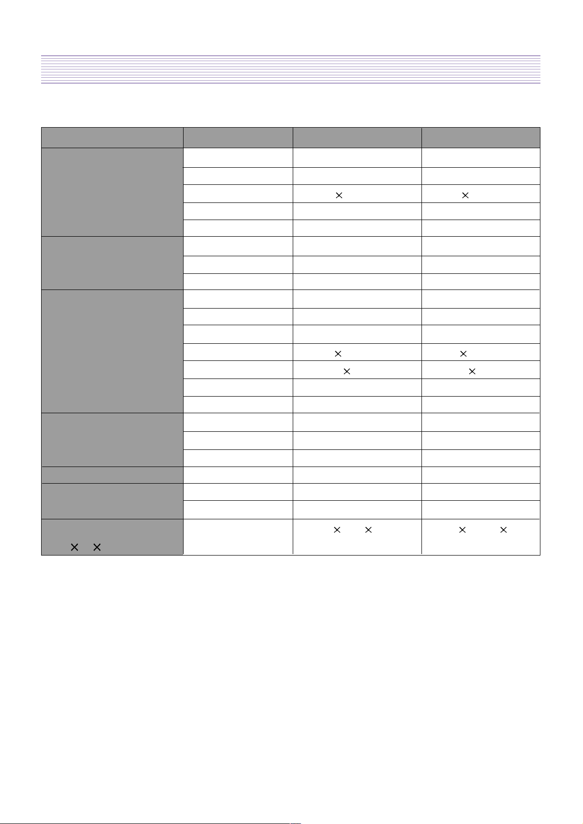
2. Product Specification
2-1. SPECIFICATION
DLP-2612 DLP-3212
LCD Panel
Screen Size 26” 32”
Aspect Ratio 16:9 16:9
Resolution 1366 768 (WXGA) 1366 768 (WXGA)
Pixel Pitch 0.4215mm 0.51075mm
Contrast Ratio 800:1 800:1
TV System Receiving System PAL, SECAM PAL, SECAM
Stereo System 2-Carrier/NICAM 2-Carrier/NICAM
Channel Memory 99ch, Auto Preset 99ch, Auto Preset
INPUT Connector RF 75 Ohm Coaxial 75 Ohm Coaxial
S-Video 1 1
Scart 2 2
Component RCA 2 RCA 2
PC RGB D-Sub 1 D-Sub 1
PC Audio 3.5mm Mini-Jack 3.5mm Mini-Jack
DVI 1 1
OUTPUT Connector Monitor-out 1 1
Headphone 3.5mm Mini-Jack 3.5mm Mini-Jack
RF-out 1 1
SOUND OUTPUT 8W 8W
Power Consumption Max. 140W 170W
Power Source 220-240V~50Hz 220-240V~50Hz
Dimension Set Dimension (850 518 231)mm (990 588.5 231)
(W H D) (Contain Stand)
-5-
2-2. Available Input Signal
RESOLUTION V-freq DVI D-SUB COMPONENT REMARK
640 480 60 IBM, VGA
66 APPLE, MAC66
72 VESA
75 VESA
720 400 70 IBM, VGA
85 IBM, XGA2
800 600 60 VESA
75 VESA
85 VESA
832 624 74 MAC74
1024 768 60 VESA
70 VESA
720P(1280 720) 50
60
1080i(1920 1080) 50
60
576P(704 576) 50
480P(720 480) 60
576i(704 576) 50
480i(720 480) 60
(2) VIDEO
- PAL, PAL-M, PAL-N
- NTSC, NTSC4.43
- SECAM
(1) PC/DVI/COMPONENT
-6-
Not Used
LCD 26", 32" (Europe ))
Block Diagram
DVI
D-SUB
COMPONENT1
SOUND1
SCART 2
AV1
SCART 1
S-VHS
PC(L,R)
Si1 169Si1 169
DVI RXDVI RX
TMDS
INPUT
BA7657BA7657
SWSW
MSP3410MSP3410
SOUND PROCESSORSOUND PROCESSOR
MST9883MST9883
AD CONVERTERAD CONVERTER
VPC3230VPC3230
COLOR DECODERCOLOR DECODER
PI5V330PI5V330
SWSW
PCF8574PCF8574
I/O
PCF8591PCF8591
AD/DAAD/DA
EL-LV385EL-LV385
LVDS TXLVDS TX
PANELPANEL
(SS/AUO)(SS/AUO)
TDA7480TDA7480
R
TDA7480TDA7480
L
R, G, B, H, V
8M8M
SDRAMSDRAM
8M8M
SDRAMSDRAM
PANEL TV VSPPANEL TV VSP
PANEL TV SVPPANEL TV SVP
3D COMB/3D COMB/
COLOR DECODER/COLOR DECODER/
DE-INTERLADER/DE-INTERLADER/
SCALER/SCALER/
GUI/PIP/POPGUI/PIP/POP
DIGITALDIGITAL
IMAGEIMAGE
CXA1855CXA1855
AUDIO/VIDEO SWAUDIO/VIDEO SW
SW1
PC L,R
24 BIT R, G, B
24 BIT R, G, B
8 BIT
H, V, CLK
H, V, CLK
H, V, CLK
SDA5, SCL5
SDA5, SCL5
MSP RESET
SDA 5550MSDA 5550M
MICOMMICOM
512K BYTE512K BYTE
FLASHROMFLASHROM
CVBS, Y, C OUT1
CVBS3, Y3, C3,
R3, L3
MONITOR CVBS OUT3
L
R
MAIN L,R
MONITOR
L, R
MONITOR L, R
CVBS2, R2, L2
RF CVBS OUT
SIF
CVBS1, Y1, C1, R1, L1
MAIN L, R
COMP1 L, R
RF L, R
RF L, R
24BIT R, G, B,
H, V, CLK
SVP RESET
PC L,R
Y, C, CVBS OUT2
VPC RESET
R, G, B, FB
TTX R, G, B, FB
R, G, B, FB
SW2
SDA5, SCL5
8BIT
PARALLEL
SDA5, SCL5
SDA33,
SDA5, SCL5
POWER FAIL
MSP_VDD5 (HP_ID)
S/SW1
S/SW2
8
Y, Cb, Cr
CVBS, H, V
AFT
SUB L, R
POWER
DOWN
MUTE
SW1
SW2
MSP_RESET
VPC RESET
BLK ON
DIMM PWM
MUTE
LCD ON
PS
SDA5,
SCL5
2005.09.09
HP L,R
HP(L,R)
HP ID
RF CVBS
KEY
IR
SVP RESET
POWER DOWN
Y, Cb, Cr
or
R, G, B, H,
J-L003J-L003
JEPICOJEPICO
VIDEOVIDEO
ENHANCEMENTENHANCEMENT
SDA 6000SDA 6000
TELETEXTTELETEXT
16M BIT16M BIT
FLASHROMFLASHROM
2M BYTE2M BYTE
SDRAMSDRAM
COMPONENT2
SOUND2
Y, Cb, Cr
MAIN
TUNER
SUB
TUNER
AFT
PI5V330PI5V330
SWSW
Y1,Cb1,Cr1
COMP2 L, R
COMP1
L, R
SUB CVBS
SW3
COMP2
L, R
Y2,Cb2,Cr2
MONO
PCF8574PCF8574
I/O
SDA5, SCL5
SW3
SPI
(CSB, JCLK, SI, SO)
4
S/SW2
S/SW1
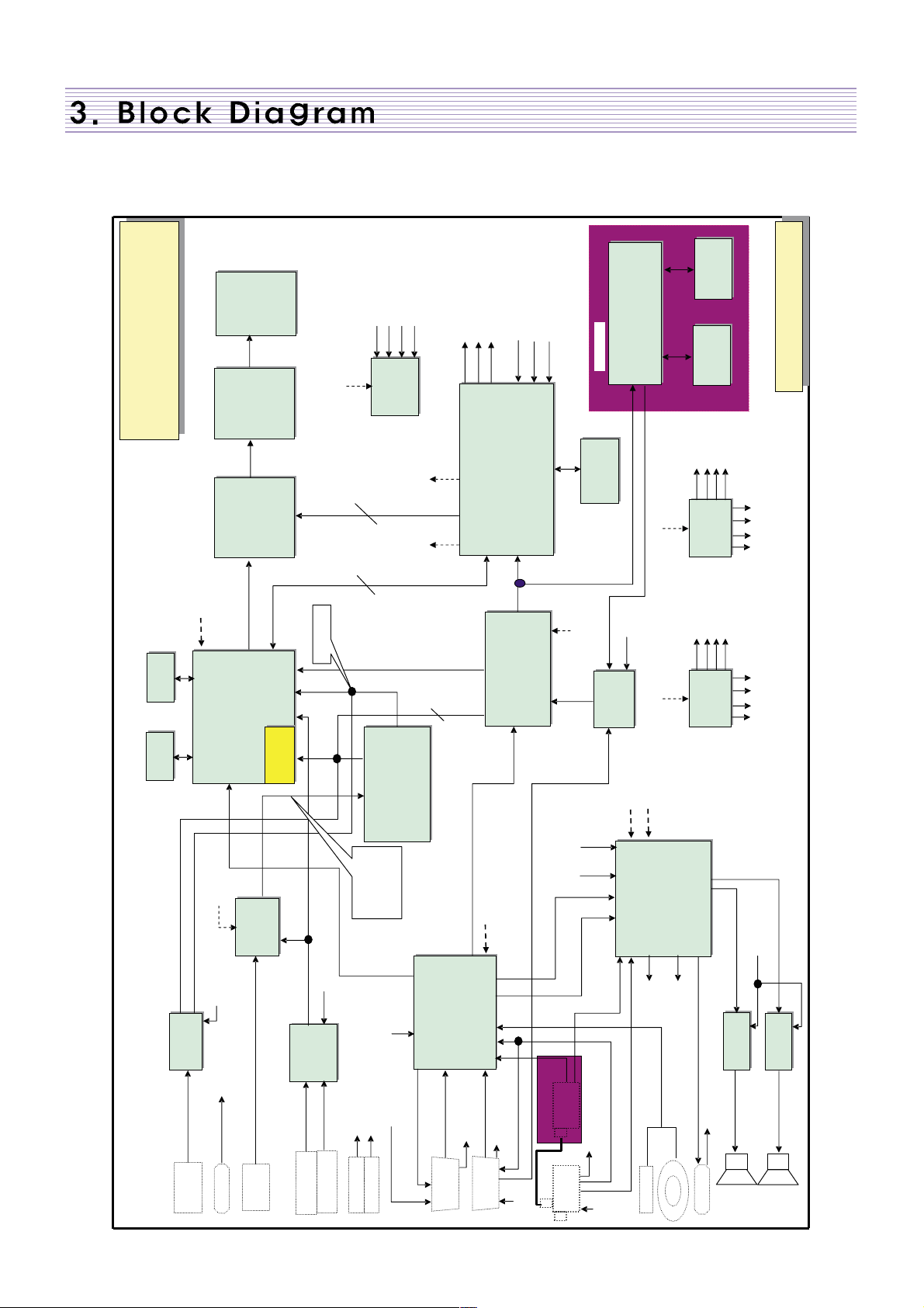
3-1. MAIN BLOCK DIAGRAM
-7-
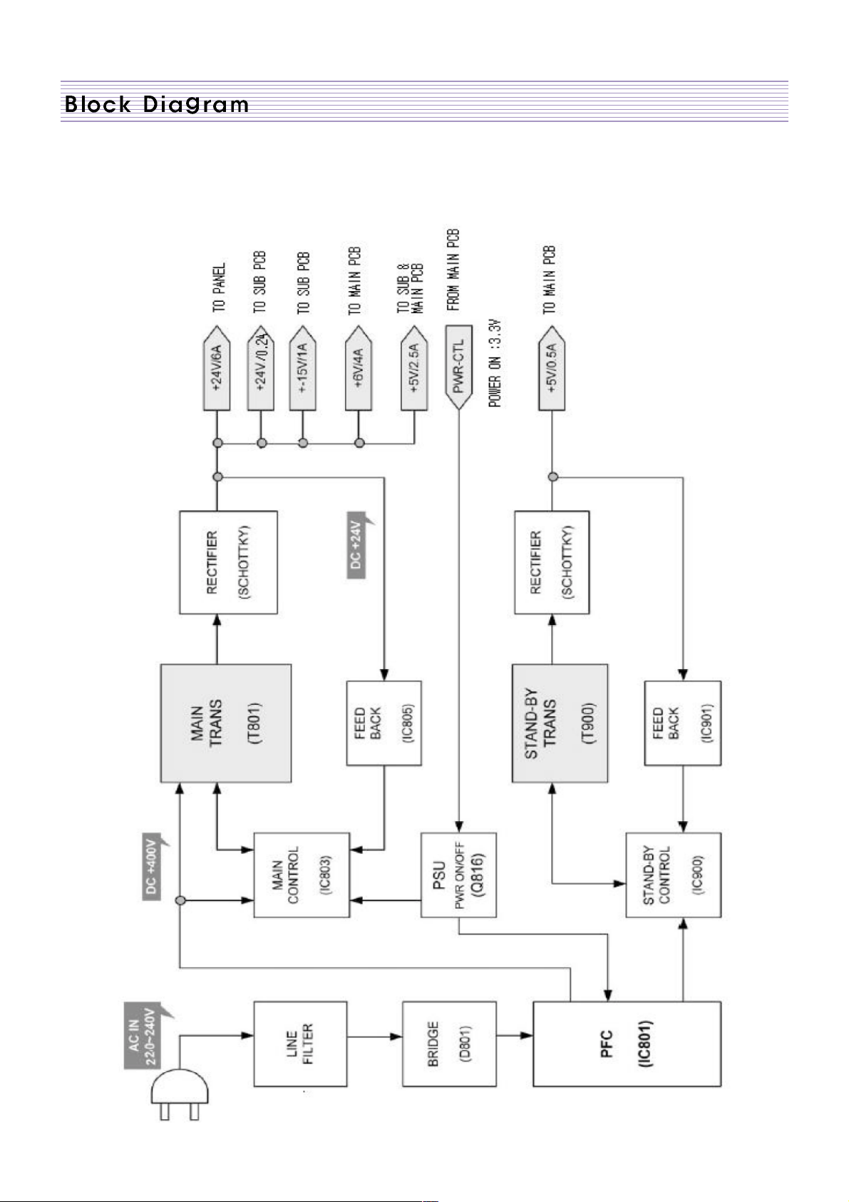
3-2. POWER BLOCK DIAGRAM
-8-
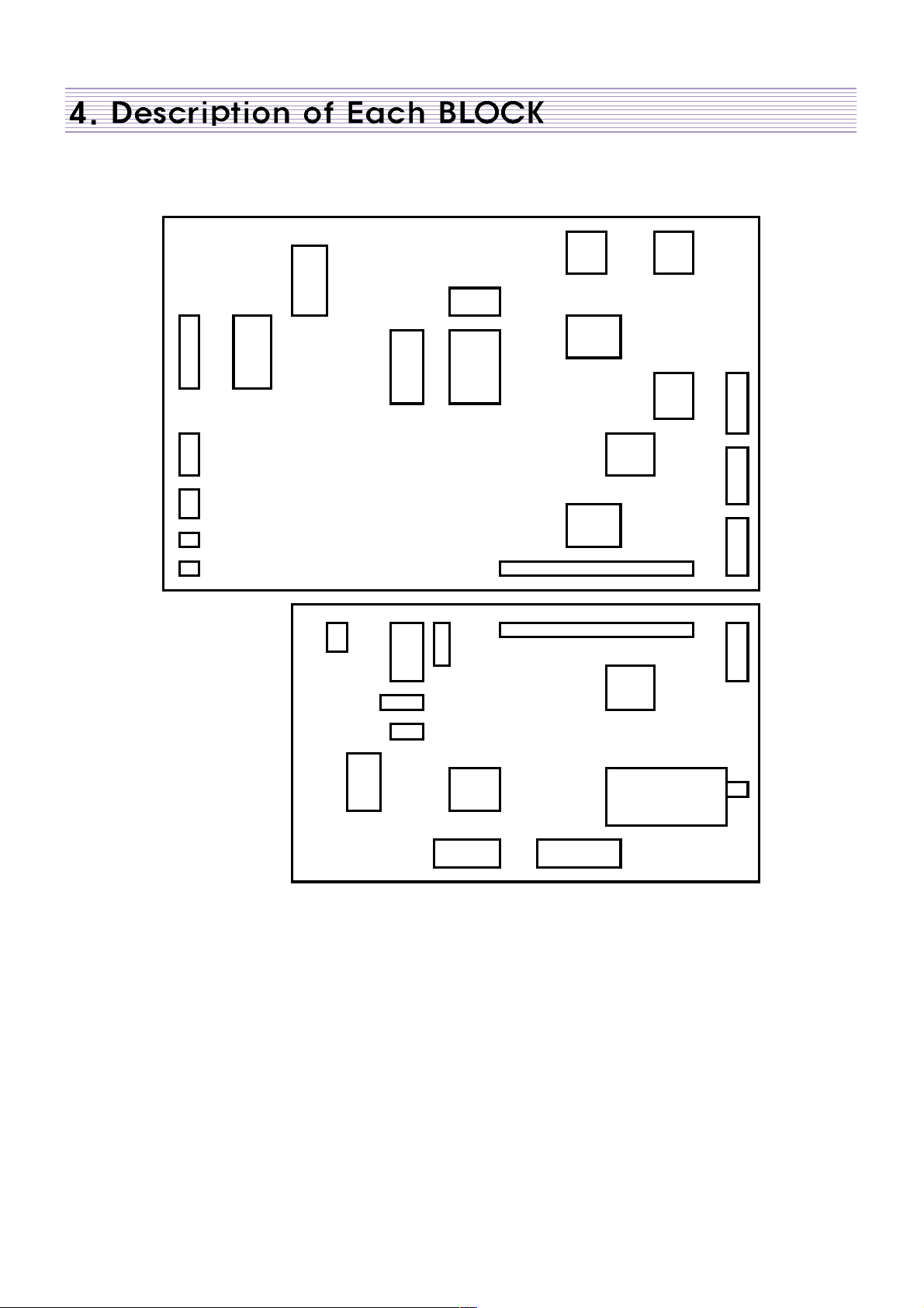
TP564
TP565
TP566
ICS2
TP603
TP604
TP605
PW30
TP159
TP160 JP11
TP161 TP246
PW11 TP162 TP247
TP248
JP12
PW12 TP494 TP508
TP495 TP509
PW7 TP496 TP529
PW15 JP3
PW6
PW21 PW20
P204
TP56 TP63
TP149 TP100 TP57 TP64
P601 TP101 TP58 TP67
TP144 TP102
PW602 TP103
TP143 TP120 TP104
TP121 TP105
TP106
TP107
TP108
TP141 TP109
JP201 JP202 TP27
TP29
TP19
IC201
IC604
IC603
TU1
ICA10
ICV10
JP206
IC601
ICU3
ICD10
ICL10
ICJ10
ICS3 ICS1
ICU10
ICU2
4-1. Block Diagram of main IC and TP
4-2. Overview
A/V block (Main and Sub PCB) is Multi Media circuit board that can process various input
signals such as video, component, PC, DVI, and analog TV signal. It is mainly composed
of switching, sync processing, decoding, analog TV, digital image processing, and system
control part.
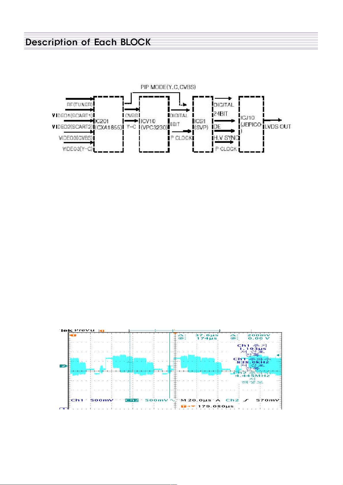
4-2-1. Composite video, Y/C(S-Video) and SCART(CVBS, RGB) composite video
Y/C(S-Video) and SCART(CVBS) have similar signal paths. For the Main signal, IC201
receives these inputted signals and switches out a selected signal. Then the signal goes
into ICV10 for video processing, SCART(RGB) signal goes directly into ICV10. The output
of ICV10 goes through ICS1 for de-interlacing and digital image processing respectively.
However, at PIP mode, sub signal has a little bit different path from the Main signal. First of
all, IC201 receives input signals such as composite video, Y/C or etc, and switches out the
selected signal like as the Main signal. But the selected signal goes into ICS1 for video
processing and image processing instead of going into ICV10.
-9-
- Main Signal
A. IC201 : Switching IC (Input: analog inputs, Output:: an analog output)
B. ICV10 : Color Decoder (Input: Y/C, CVBS, R/G./B, Output: 8bit digital, H/V)
C. ICS1 : Color Decoder/Image Processor(Input: 8bit Digital or 24bit Digital R/G/B,
H/V,Output: 24bit Digital R/G/B, H/V)
-Main TP (Input: Color Bar Pattern)
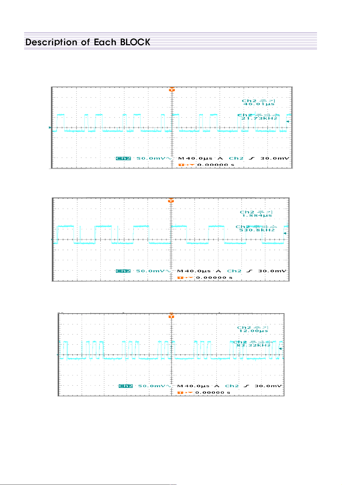
★CCV15(Y Signal), CCV14(C Signal), CCV16(CVBS Signal)
★RCS12(Horizontal sync), RCS13(Vertical sync), RCS14(Clock) RCS15(Data enable)
-Sub Signal(In PIP mode)
A. IC201: Switching IC (Input: analog inputs, Output: an analog output)
B. ICS1: Color Decoder/Image Processor (Input: 8bit Digital or 24bit Digital R/G/B,
H/V,Output: 24bit Digital R/G/B, H/V)
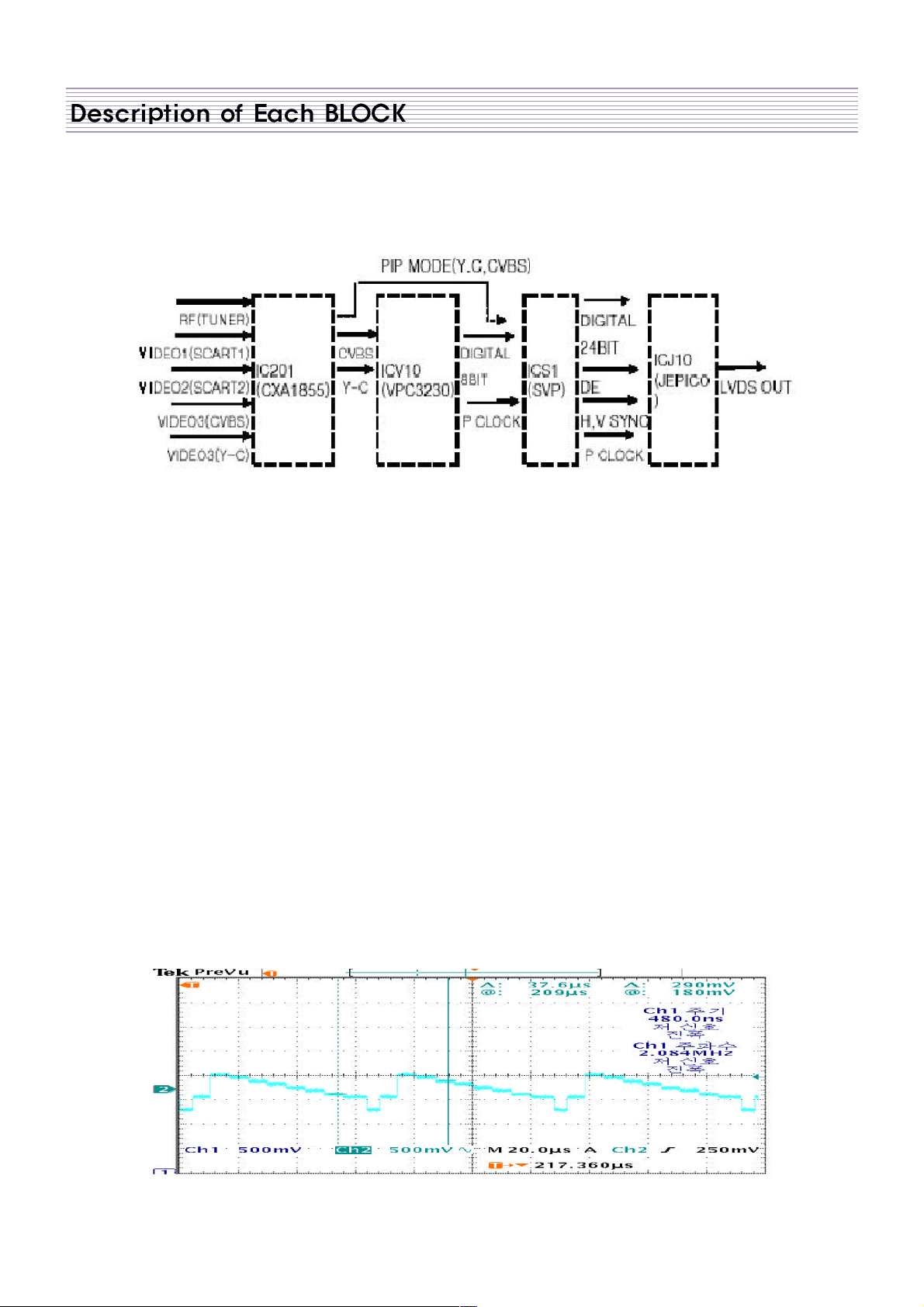
Y signal (input to ICV10)
Location: LCV13
-Flow Chart of RF, Video, S-Video Signal
-10-
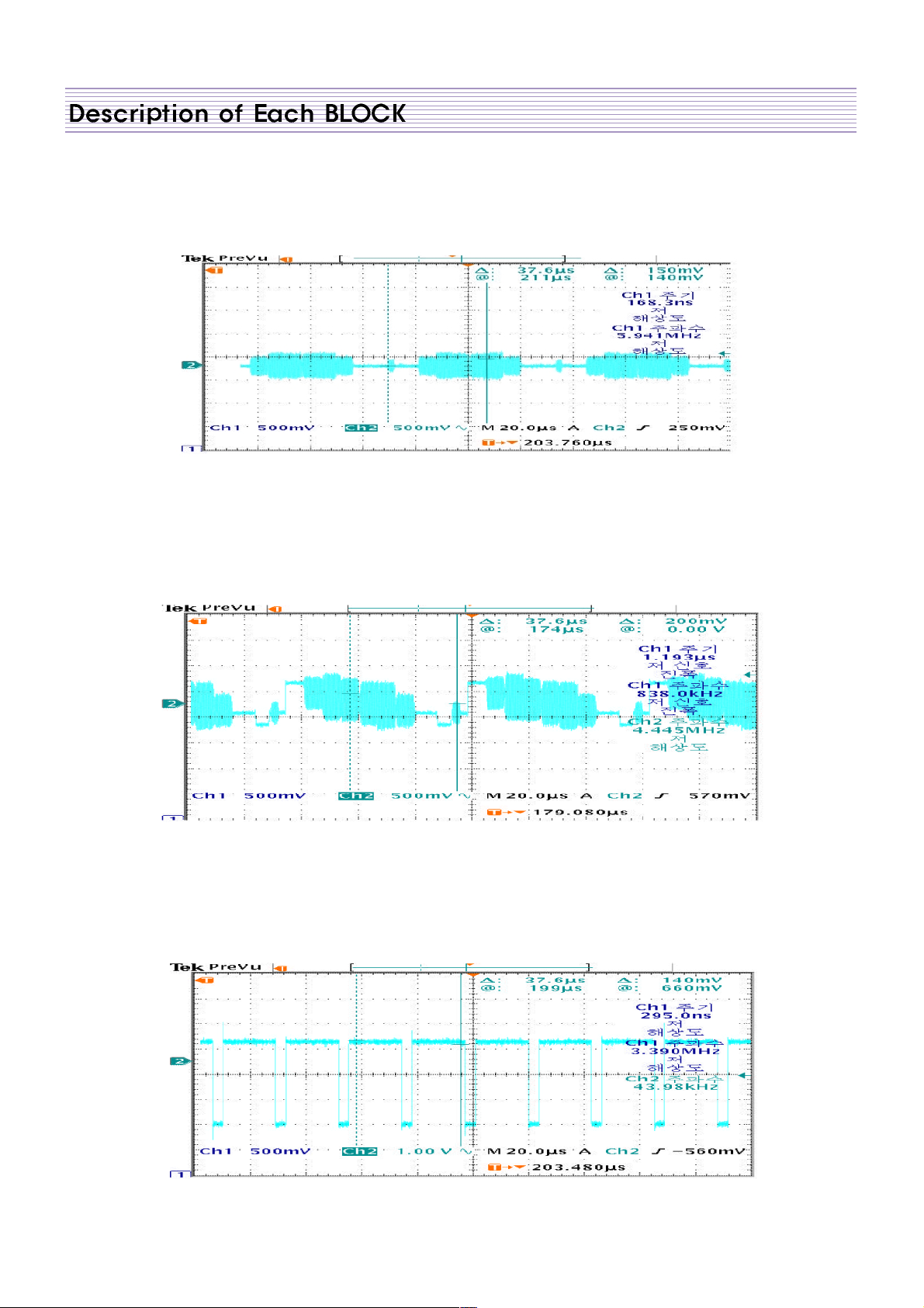
Color signal (input to ICV10)
Location: LCV4
CVBS signal (Input to ICV10)
Location: LCV1
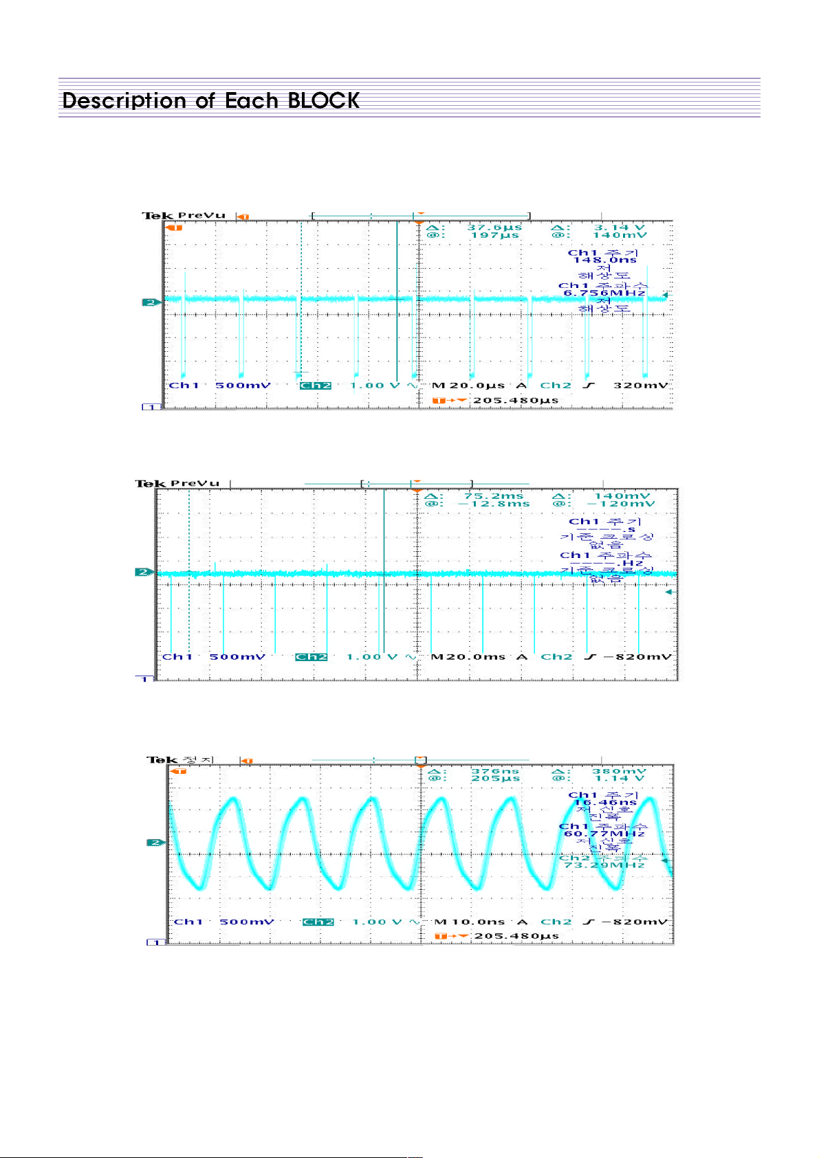
Data Enable(Output of ICS1)
Loacation(RCS15, ICD10.73PIN)
-11-
Horizontal sync (Out of ICS1)
Location: RCS12, ICD10.72PIN
Vertical sync (Out of ICS1)
Location: RCS13, ICD10.71PIN
Clock for display (Out of ICS1)
Location: RCS14, ICD10.76PIN
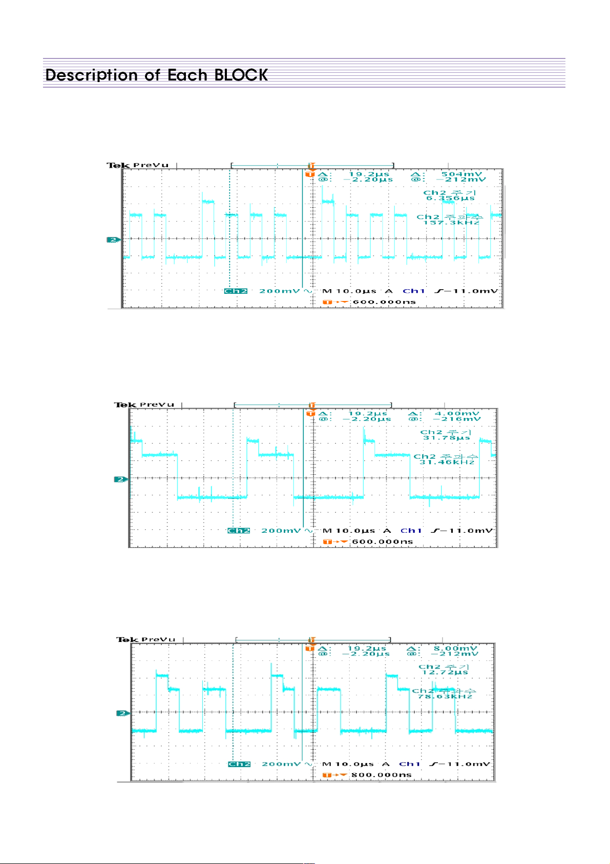
4-2-2. TV signal
Tuner(TU1) receives antenna signal and outputs CVBS and sound signal. For the main
signal, IC201 switches out the CVBS and the rest of the signal flow is same as composite
video signal flow mentioned earlier.
Also, Sub TV signal at PIP mode flows similar path to the Sub composite video signal pass
except that IC201 switches out the CVBS signal
-12-
- Flow Chart of RF CVBS
- Main Signal
A. TU1 : Tuner (Input: antenna signal, Output: CVBS)
B. IC201 : Switching IC (Input: CVBS, Output: CVBS)
C. ICV10 : Vided processor (Input: CVBS, Output: 8bit Digital, H/V)
D. ICS1 : Color Decoder/Image Processor(Input: 24bit Digital R/G/B, H/V, Output: 24bit
Digital R/G/B, H/V)
- Sub Signal(In PIP mode)
A. IC201 : Switching IC (Input Input: antenna signal, Output: CVBS)
B. ICS1 : Color Decoder/Image Processor(Input: 24bit Digital R/G/B, H/V, Output: 24bit
Digital R/G/B, H/V)
- Main TP (Input: Color Bar Pattern)
★ CE220, CCV16
★ RCS12(Horizontal sync), RCS13(Vertical sync), RCS14(Clock) RCS15(Data enable)
CVBS signal (Input to IC201)
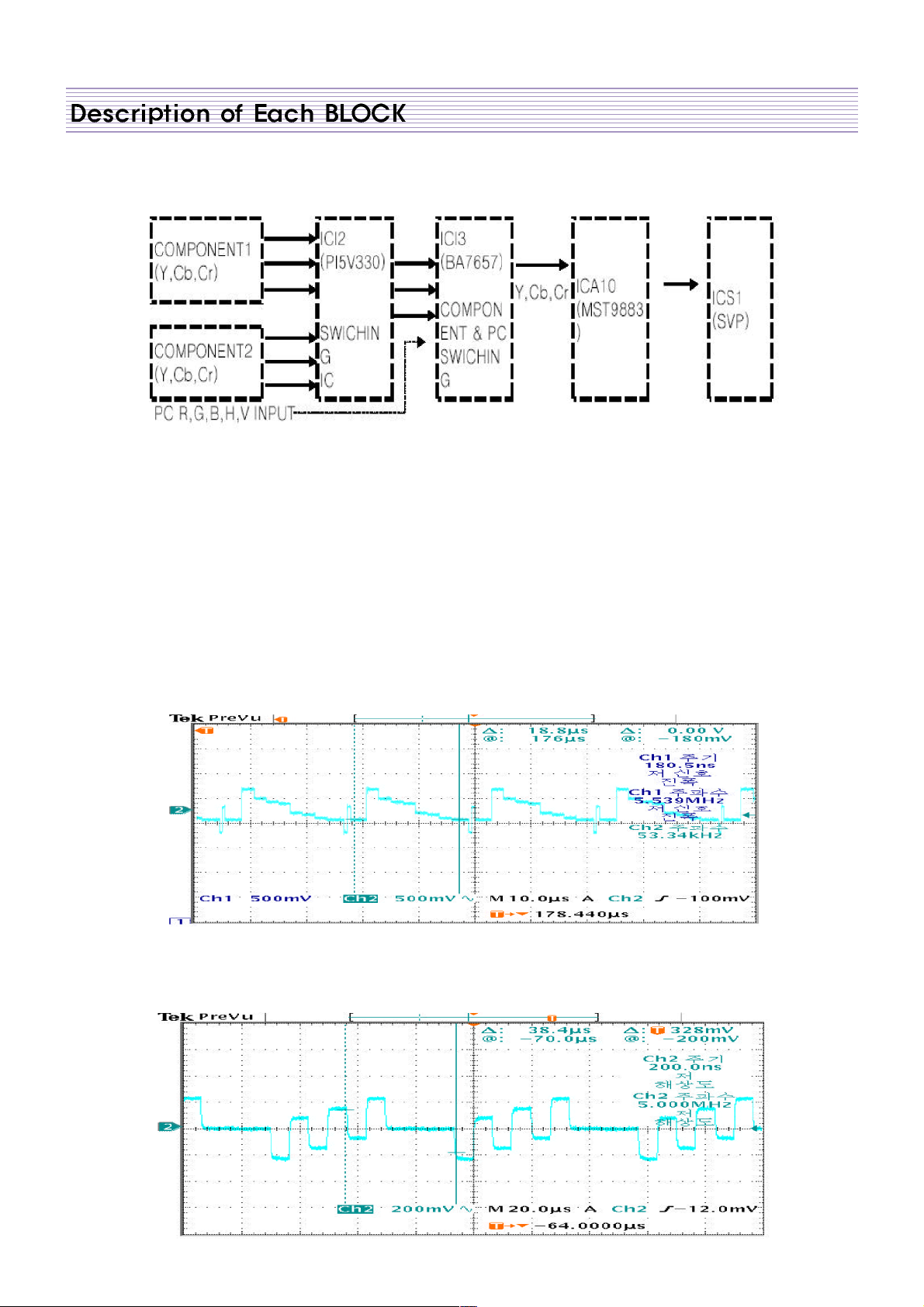
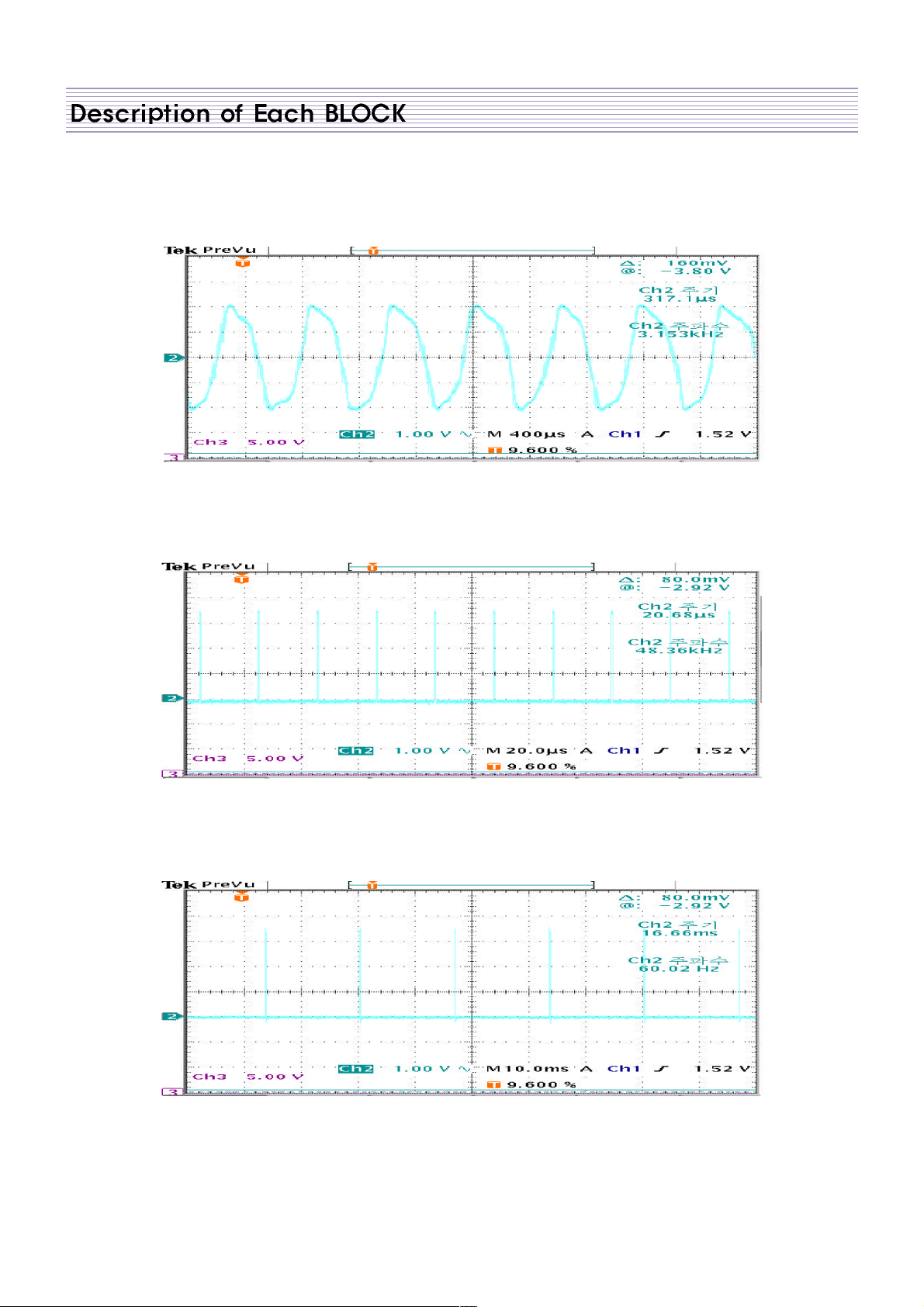
4-2-3. DTV/DVD signal
Both DTV(Y, Pb, Pr) and DVD(Y, Cb, Cr) share same jack and signal path. Main and Sub in
PIP mode have same path. ICI3 switches out signal and also detects type of signal so that
ICA10 can convert the analog signal to digital. Then the signal goes through ICS1 for the
image processing.
-13-
- Flow Chart of COMPONENT
Y signal (Input to ICA10)
Location: LCA4, RCA12
Pb Signal (Input to ICA10)
Location: LCA5, RCA14
- Main Signal
A. ICI3 : Switching IC (Input: Component, Output: Component, H/V)
B. ICA10 : A/D converter (Input: Component, H/V, Output: 24bit Digital RGB, H/V)
C. ICS1 : Color Decoder/Image Processor(Input: 24bit Digital R/G/B, H/V,Output: 24bit
Digital R/G/B, H/V)
- Main TP (Input: 576I, Color Bar Pattern)
-14-
Pr Signal (Input to ICA10)
Location: LCA3, RCA11
Clock (Output of ICA10)
Location: LCA1, RCA10
Horizontal sync (Output of ICA10)
Location: RCA9
-15-
Vertical sync (Output of ICA10)
Location: RCA8
4-2-4. PC (Personal Computer) signal
PC signal is switched out by ICI3 and input to ICA10 for A/D conversion. Then the signal
goes through ICS1 for digital image processing.
- Flow Chart of PC Signal
- Main IC
A. ICI3 : Switching IC (Input: Analog RGB, H/V, Output: Analog RGB, H/V)
B. ICA10 : A/D converter (Input: Analog RGB, H/V, Output: 24bit Digital RGB, H/V)
C. ICS1 : Color Decoder/Image Processor(Input: 24bit Digital R/G/B, H/V, Output: 24bit
Digital R/G/B, H/V)
- Main TP (Input: Color Bar Pattern, 1024X768 60Hz)
-16-
R Signal (Input to ICA10)
Location: LCA3, RCA11
G Signal (Input to ICA10)
Location: LCA4, RCA12
B Signal (Input to ICA10)
Location: LCA5, RCA14
-17-
Clock (Output of ICA10)
Location: LCA1, RCA10
Horizontal sync (Output of ICA10)
Location: RCA9
Vertical sync (Output of ICA10)
Location: RCA8
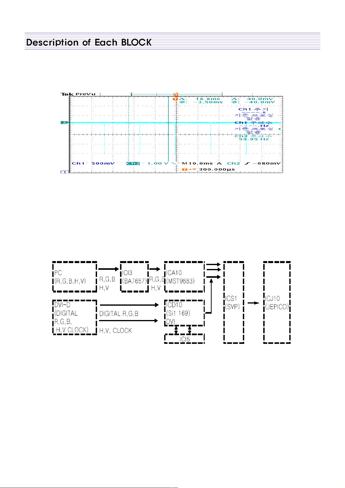
4-2-5 DVI (Digital Visual Interface) signal
To process DVI signal, graphic card of AV device reads EDID data from ICI5(ROM). Then
DVI signal is directly inputted to ICD10, which output digital 24bit RGB and H/V. The output
goes through ICS1 for digital image processing
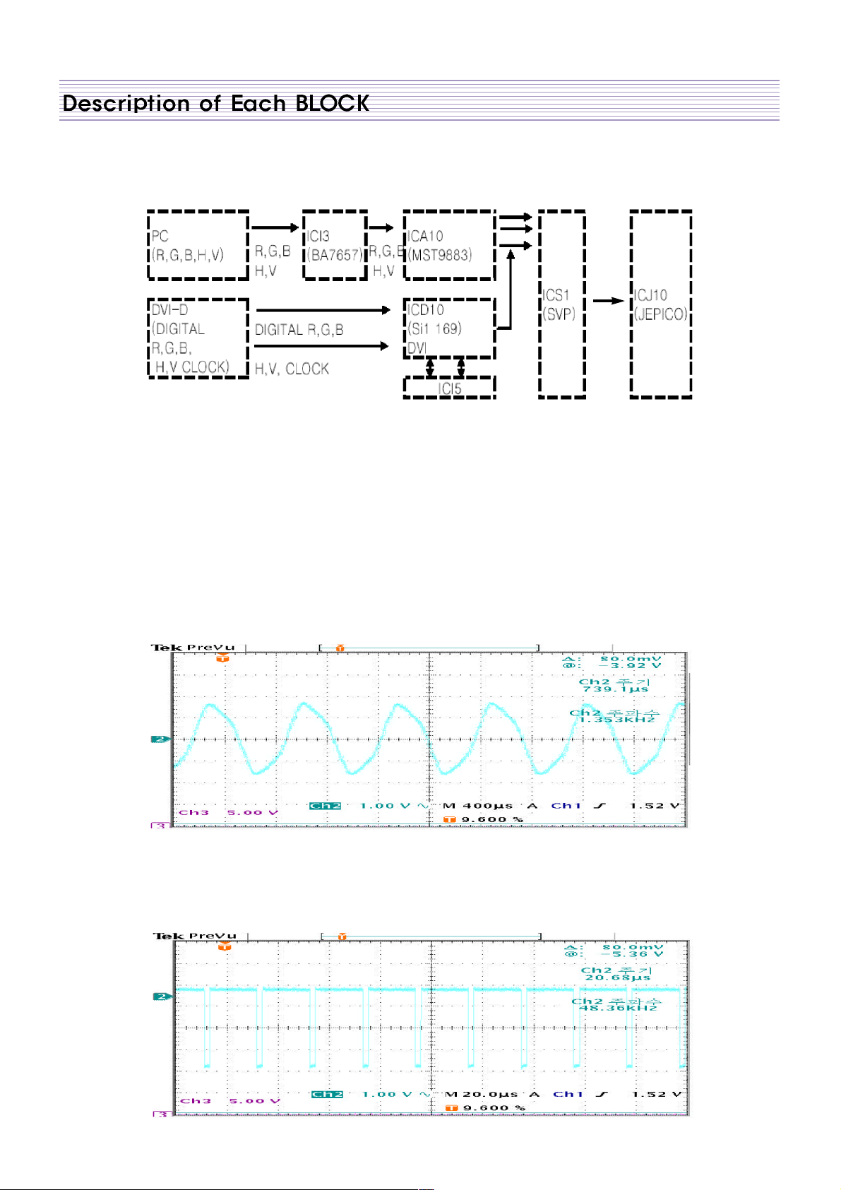
-18-
- Flow Chart of DVI Signal
- Main IC
A. ICI5 : ROM containing EDID data (EDID: display capabilities such as resolution, aspect
ratio etc.)
B. ICD10: DVI signal processor (Input: TMDS, Output: 24bit digital RGB, H/V)
- Main TP (Input: Color Bar Pattern)
Clock (Output of ICD10)
Location: LCD5, RCD5
Horizontal sync (Output of ICD10)
Location: RCD6
- Main IC
A. ICI5 : ROM containing EDID data (EDID: display capabilities such as resolution, aspect
ratio etc.)
B. ICD10: DVI signal processor (Input: TMDS, Output: 24bit digital RGB, H/V)
- Main TP (Input: Color Bar Pattern)
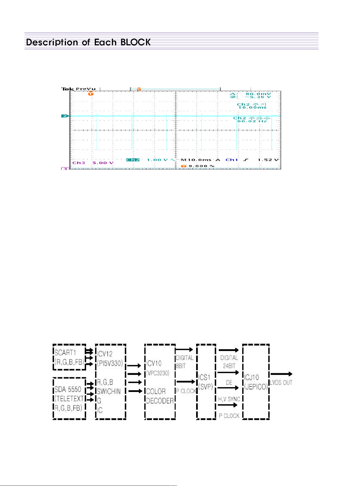
-19-
Vertical sync (Output of ICD10)
Location: RCD7
4-2-6. Video Enhancer and LVDS transmitter (for all inputs)
Outputs of ICS1 are inputted to ICJ10(Video signal enhancer, MGDI) which improves
picture quality greatly.
Outputs of ICJ10 are inputted to ICL10 which is a LVDS transmitter. The converted LVDS
signal is transmitted to the LCD panel.
- Main IC
A. ICJ10: Video enhancer (Input: 24bit digital RGB, H/V Output: 24bit digital RGB, H/V)
B. ICL10: LVDS transmitter (Input: 24bit digital RGB, H/V Output: LVDS signal)
- Main TP
★ RCJ2: Horizontal sync (Output of ICJ10), refer to RCS12
★ RCJ3: Vertical sync (Output of ICJ10), refer to RCS13
★ RCJ1 : Data Enable sync (Output of ICJ10), refer to RCS15
4-2-7. R/G/B PROCESSING (SCART1, TELETEXT R/G/B)
- Flow Chart of SCART1, TELETEXT R/G/B
- Main TP
-20-
R Signal (Input to ICV10)
Location: LCV10, RCV30
G Signal (Input to ICV10)
Location: LCV9, RCV28
B Signal (Input to ICV10)
Location: LCV8, RCV26
4-2-8. Audio signal processing, KEY, and LED
IC201 switches Audio signals and passes a switched signal to IC601 for audio signal
processing. IC601 controls sound parameters such as Volume, Balance, and Equalize.
-21-
- Flow Chart of Audio Signal
- Main IC
A. IC201: Switching IC
B. IC601: Audio processing IC
C. IC603,604: Amplifying IC
MSP3410 INPUT
Location
- Main R sound: CE620, RC621 - Main L sound: CE619, RC620
- Sub R Sound: CE618, RC619 - Sub L Sound: CE617, RC618
- Component1 R sound: CE616, RC617 - Component1 L sound: CE615, RC616
- Component2 R sound: CE614, RC615 - Component2 L sound: CE613, RC614
PC_L Sound (Input to IC201)
Location (CE208, RC253)
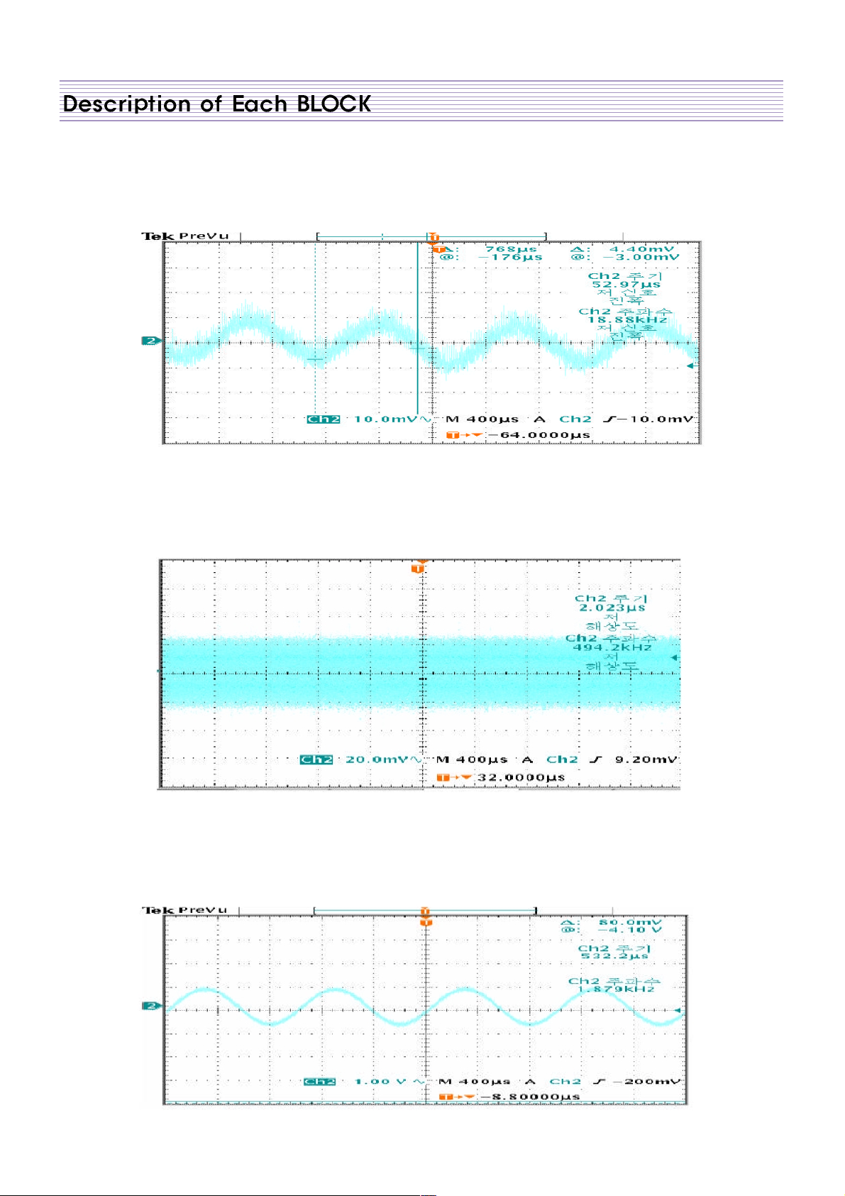
The outputs of IC601 are passed to IC604(right), and IC603(left) respectively to amplify
the signals. KEY and LED PCBs send signals received from key buttons and LED to
ICU10 for command processing.
-22-
IC604, 605 INPUT
Location: L out(CE605), R out(CE604)
Tuner SIF Input
Location: CC613, TU1.9PIN
HEADPHONE Out
Location: CE636, CE639
-23-
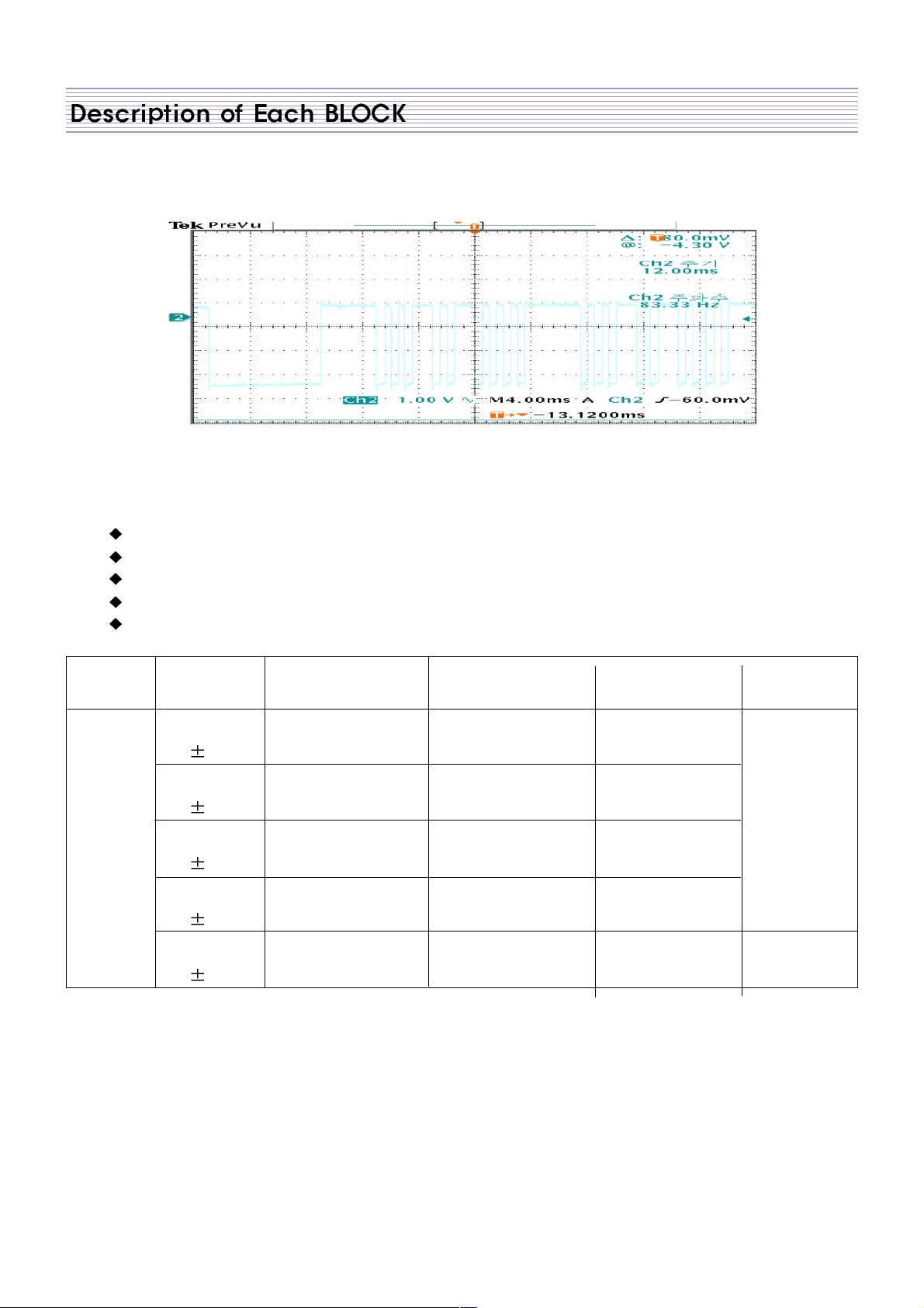
Remote control signal
Location: RCW17, CCW3
4-3. POWER PCB
4-3-1. POWER SPEC
Rating: 220V~240V
Regulating Method:
Input Frequency: 50Hz
Inrush Current: Below 80A at AC230V
Output Voltage and Current are shown below
Board
Output Minimum output Maximum output Output Current
Condition
Voltage voltage voltage Continuous
+24Vdc
+22.8Vdc +25.2Vdc
0-6.0A
(
5%) (144Watt)
+15Vdc
+14.25Vdc +15.75Vdc
0-1.0A
( 5%) (30Watt) PWR-CTL
DEP +6Vdc
+5.7Vdc +6.3Vdc
0-4.0A ON
( 5%) (24Watt)
+5Vdc
+4.75Vdc +5.25Vdc
0-2.5A
( 5%) (12.5Watt)
ST+5Vdc
+4.75Vdc +5.25Vdc
0-1.0A PWR-CTL
( 5%) (5Watt) OFF
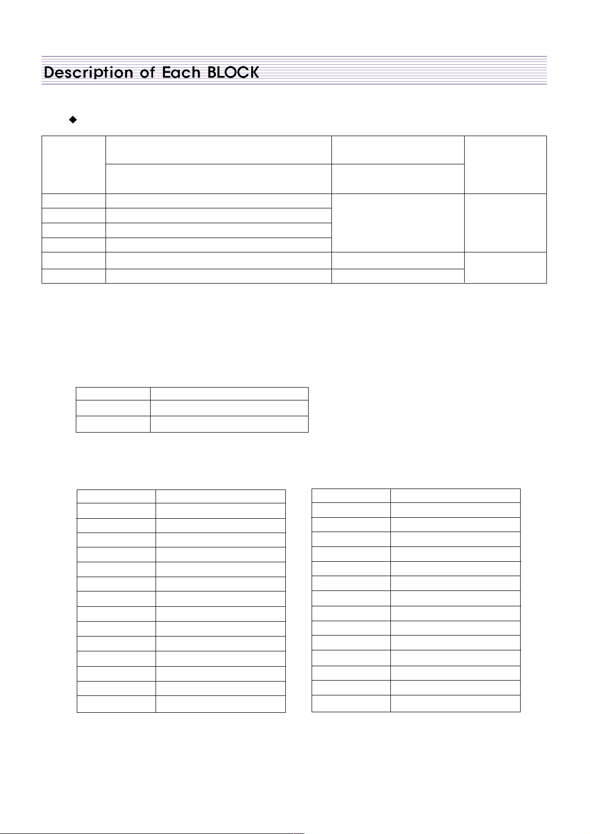
-24-
Ripple and Noise
Output
Output voltage
AC ripple, Switching
Condition
ripple and noise
Name Minimum output Maximum output
Continuous
voltage voltage
+24V 22.8Vdc 25.2Vdc PWR-CTL
+15V 14.25Vdc 15.75Vdc 500mVp-p ON
+6V 5.7Vdc 6.3Vdc Max Load
+5V 4.75Vdc 5.25Vdc
ST+5V 4.75Vdc 5.25Vdc 500mVp-p PWR-CTL
Other Lines Don’t Care OFF
4-3-2. Connectors
A. AC Connectors
P801 (I-SHENG PLASTIC 7003 7.0MM 3P)
Power Switch Connector
P802 (YEON-HO YDW236-02P)
PIN NO. CONFIGRATION
1 LIVE Switch PIN1
2 LIVE Switch PIN2
B. PL11, PL12 pin Spec (HAN JUN A2002WV2-14P 14p)
PIN NO. OUT PUT
1 +24V
2 +24V
3 +24V
4 +24V
5 +24V
6 GND
7 GND
8 GND
9 GND
10 GND
11 Not Connected
12 INV ON/OFF
13 GND
14 PWM-DIMMING
PL11(SAMSUNG PANNEL)
PIN NO. OUT PUT
1 +24V
2 +24V
3 +24V
4 +24V
5 +24V
6 GND
7 GND
8 GND
9 GND
10 GND
11 GND
12 INV ON/OFF
13 PWM-DIMMING
14 GND
PL12(AUO)
 Loading...