

Page 1

Service Manual
TFT LCD MONITOR
Model : L500B
DAEWOO ELECTRONICS CO., LTD
OVERSEAS SERVICE DEPT.
Page 2

TABLE OF CONTENTS
SAFETY PRECAUTIONS ................................................................................................. 2
GENERAL SAFETY INFORMATION.................................................................................. 3
SERVICING PRECAUTIONS........................................................................................... 4
GENERAL INFORMATION............................................................................................. 8
PIN CONNECTOR ....................................................................................................... 9
OPERATION & ADJUSTMENT ........................................................................................ 10
ALIGNMENT PROCEDURE............................................................................................ 14
TROUBLE SHOOTING HINTS.......................................................................................... 15
BLOCK DIAGRAM ....................................................................................................... 22
PCB LAYOUT ............................................................................................................... 23
SCHEMATIC DIAGRAM................................................................................................ 25
EXPLODED VIEW & MECHANICAL PARTS LIST................................................................ 33
INFORMATION OF PART DESCRIPTION ......................................................................... 34
ELECTRICAL PARTS LIST................................................................................................ 35
1
Page 3

SAFETY PRECAUTIONS
CAUTION
No modifications of any circuit should be attempted. Service work should only be performed after you
are thoroughly familiar with all of the following safety check and servicing guidelines.
u
Fire & Shock Hazard
w In servicing, pay attention to original lead dress especially in the high voltage circuit. if a short circuit
is found, replace all parts which have been overheated as a result of the short circuit.
w All the protective devices must be reinstalled per original design.
w Soldering must be inspected for possible cold solder points, frayed leads, damaged insulation, solder
splashes or sharp solder points. Be certain to remove all foreign materials.
u
Implosion Protection
TFT LCD in this monitor employs integral implosion protection system, but care should be taken to avoid
damage and scratching during installation.
Use only same type replacement TFT panel.
IMPORTANT SAFETY NOTICE
There are special components used in analog TFT LCD color display, which are important for safety.
These parts are shaded on the schematic diagram and on the replacement parts list. It is essential
that these critical parts should be replaced with manufacturer’s specified parts to prevent X-radiation,
shock, fire or other hazards. Do not modify the original design without getting a written permission
from DAEWOO ELECTRONICS CO. or this will void the original parts and labor warranty.
2
Page 4
GENERAL SAFETY INFORMATION
u
Terms in the manual
CAUTION Statements identify conditions or practices that could result in damage to the equipment or
other property.
WARNING Statements identify conditions or practices that could result in personal injury or loss of life.
u
Terms as marked on equipment
CAUTION Statements indicate a personal injury hazard not immediately accessible as one reads the
marking, or a hazard to properly including the equipment itself.
WARNING Statements indicate a personal injury hazard immediately accessible as one reads the marking
u
Symbols in the manual
This symbol indicates where applicable cautionary or other information is to be found.
u
Symbols as marked on equipment
Protective GROUND terminal
u
High Voltage Warning And Critical Component Warning Label
Following warning label is on the backlight outside.
WARNING
This product includes critical mechanical and electrical parts. For continued safety, replace critical
components indicated in the service manual only with exact replacement parts given in the parts list.
Refer to service manual for measurement procedures and proper service adjustments.
3
Page 5
SERVICING PRECAUTIONS
CAUTION
Before servicing instruments covered by this service manual, its supplements and addendum, read
and follow the SAFETY PRECAUTIONS of this manual.
NOTE
If unforeseen circumstances create conflict between the following servicing precautions and any of
the safety precautions on page 1 of this manual, always follow the safety precautions.
Remember: Safety First.
u
General Servicing Precautions
1. Always unplug the AC power cord from the AC power source before:
a. Removing or reinstalling any component, circuit board, module, or any other instrument assembly.
b. Disconnecting or reconnecting any electrical plug or other electrical connection.
c. Connecting a test substitute in parallel with an electrolytic capacitor in the instrument.
CAUTION
A wrong part substitution or incorrect polarity installation of electrolytic capacitors may result in a
explosion hazard.
2. Do not any spray chemicals on or near this instrument or any or its assemblies.
3. Unless specified otherwise in this service manual, clean electrical contacts by applying the following
mixture to the contacts with a pipe cleaner, cotton-tipped stick or comparable nonabrasive applicator:
10% (by volume) Aceton and 90% (by volume) isopropyl alchohol (90%-99% strength).
CAUTION
This is a flammable mixture. Unless specified otherwise in this service manual, lubrication of contacts
is not required.
4. Do not apply AC power to this instrument and/or any of its electrical assemblies unless all solid-state
device heat sinks are correctly installed.
5. Always connect the test instrument ground lead to the appropriate instrument chassis ground before
connecting the test instrument positive lead. Always remove the test instrument ground lead last.
6. Use only the test fixtures specified in this service manual with this instrument.
CAUTION
Do not connect the test fixture ground strap to any heatsink in this instrument.
4
Page 6

SERVICING PRECAUTIONS
u
Electrostatically Sensitive (ES) Devices
Some semiconductor (solid state) devices can be damaged easily by static electricity.
Such components commonly are called Electrostatically Sensitive (ES) Devices.
The examples of typical ES devices are integrated circuits, some field-effect transistors and
semiconductor “chip” components. The following techniques should be used to help reduce the
incidence of component damage caused by static electricity.
1. Immediately before handling any semiconductor component or semiconductor-equipped assembly,
drain off any electrostatic charge on your body by touching a known earth ground. Alternatively,
obtain and wear a commercially available discharging wrist strap device which should be removed for
potential shock reasons prior to applying power to the unit under test.
2. After removing an electrical assembly equipped with ES devices, place the assembly on a conductive
surface such as aluminum foil to prevent electrostatic charge buildup or exposure of the assembly.
3. Use only a grounded-tip soldering iron to solder or unsolder ES devices.
4. Use only an anti-static type solder removal device. Some solder removal devices not classified as
“anti-static” can generate enough electrical charges to damage ES devices.
5. Do not use freon-propelled chemicals. These can generate enough electrical charges to damage ES devices.
6. Do not remove a replacement ES device from its protective package until immediately before you are
ready to install it. (Most replacement ES devices are packaged with leads electrically shorted together
by conductive foam, aluminum foil or comparable conductive material).
7. Immediately before removing the protective material from the leads of a replacement ES device,
touch the protective material to the chassis or circuit assembly into which the device will be installed.
CAUTION
Be sure that no power is applied to the chassis or circuit, and observe all other safety precautions.
8. Minimize bodily motions when handling unpackaged replacement ES devices. (Otherwise harmful
motion such as the brushing together of your clothes fabric or the lifting of your foot from a carpeted
floor can generate enough static electricity to damage an ES devices).
u
General Soldering Guidelines
1. Use a grounded-tip, low-wattage soldering iron with appropriate tip size and shape that will maintain
tip temperature within a 550°F-660°F (288°C-316°C) range.
2. Use an appropriate gauge of RMA resin-core solder composed of 60 parts tin/40 parts lead.
3. Keep the soldering iron tip clean.
4. Throughly clean the surface to be soldered. Use a small wire-bristle (0.5 inch or 1.25cm) brush with a
metal handle. Do not use freon-propelled spray-on cleaners.
5. Use the following soldering technique:
a. Allow the soldering iron tip to reach normal temperature (550°F to 660°F or 288°C to 316°C)
b. Hold the soldering iron tip and solder strand against the component lead until the solder melts.
c. quickly move the soldering iron tip to the junction of the component lead and the printed circuit foil,
and hold it there only until the solder flows onto and around both the component lead and the foil.
d. Closely inspect the solder area and remove any excess or splashed solder with a small wire-bristle brush.
CAUTION
Work quickly to avoid overheating the circuit board printed foil.
5
Page 7
SERVICING PRECAUTIONS
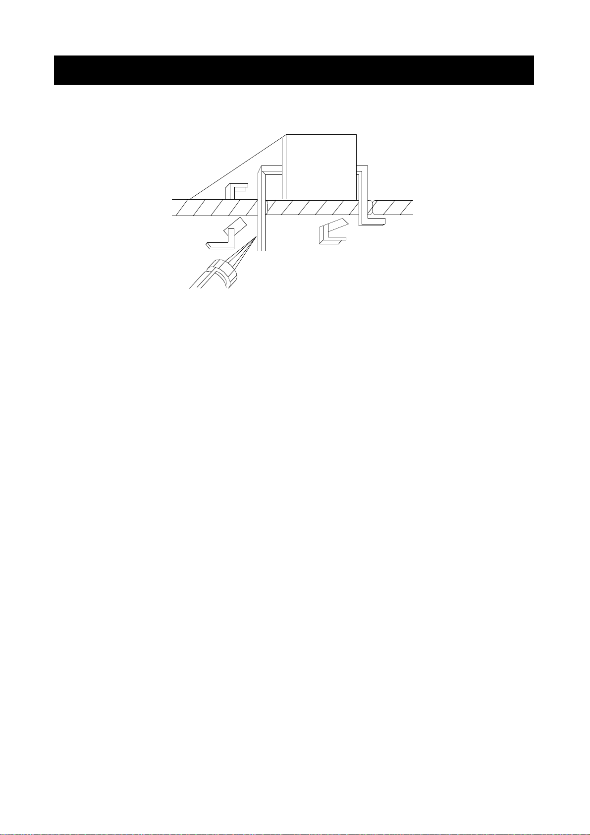
FIGURE1. USE SOLDERING IRON TO PRY LEADS
u
IC Removal / Replacement
Some utilized chassis circuit boards have slotted (oblong) holes through which the IC leads are inserted
and then bent flat against the circuit foil. When holes are slotted, the following technique should be used
to remove and replace the IC. When working with boards using the familiar round hole, use the standard
technique as outlined in paragraphs 5 on the page under the title of general soldering guidelines.
u
Removal
1. Desolder and straighten each IC lead in one operation by gently prying up on the lead with the soldering iron tip as the solder melts.
2. Draw away the melted solder with an anti-static suction-type solder removal device (or with desoldering braid before removing the IC.
u
Replacement
1. Carefully insert the replacement IC in the circuit board.
2. Carefully bend each IC lead against the circuit foil pad and solder it.
3. Clean the soldered areas with a small wire-bristle brush. (lt is not necessary to reapply acrylic coating
to the area).
u
“Small-Signal” Discrete Transistor Removal/Replacement
1. Remove the defective transistor by clipping its leads as close as possible to the component body.
2. Bend the end of each of three leads remaining on the circuit board into a “U” shape.
3. Bend the replacement transistor leads into a “U” shape.
4. Connect the replacement transistor leads to the corresponding leads extending from the circuit board
and crimp the “U” with long nose pliers to insoure metal-to-metal contact, then solder each
connection.
6
Page 8
SERVICING PRECAUTIONS
u
Power IC, Transistor or Devices Removal / Replacement
1. Heat and remove all solders from the device leads.
2. Remove the heatsink mounting screw (if applicable).
3. Carefully remove the device from the circuit board.
4. Insert new device in circuit board.
5. Solder each device lead, and clip off excess lead.
6. Replace heatsink.
u
Diode Removal / Replacement
1. Remove defective diode by clipping its leads as close as possible to diode body.
2. Bend the two remaining leads perpendicularly to the circuit board.
3. Observing diode polarity, wrap each lead out of the new diode around the corresponding lead on the
circuit board.
4. Securely crimp each connection and solder it.
5. Inspect the solder joints of the two “original” leads on the circuit board copper side. If they are not
shiny, reheat them and apply additional solder if necessary.
uTECHNICAL INFORMATION
Electrical
Pixel pitch 0.3mm X 0.3mm
Horizontal frequency 30KHz to 62KHz (Automatically)
Vertical frequency 50Hz to 85Hz (Automatically)
Operating temperature 10-40°C / 50-104°F
Operating humidity 8-80%
Mechanical
Cabinet Molded Plastic Cabinet with attachable tilt & swivel base
Dimension (set with packing) 502(H) X 502(W) X 242(D) mm
Weight(net) 4.5 Kg
Controls
Power Switch
OSD control
7
Page 9

GENERAL INFORMATION
This TFT LCD monitor automatically scans all horizontal frequencies from 30KHz to 62KHz, and all vertical frequencies from 50Hz to 85Hz. This TFT LCD monitor supports IBM PC, PC/XT, PC/AT, personal
System/2 (PS/2), Apple Macintosh, and compatible users crisp text and vivid color graphics display
when using the following graphics adapters : (VGA, Super VGA, VESA and XGA and Apple Macintosh
Video Card). And so, this TFT LCD monitor has a maximum horizontal resolution of 1024 dots and a
maximum vertical resolution of 768 lines for superior clarity of display.
By accepting analog signal inputs which level is zero to 0.7 Volts. This TFT LCD monitor can display and
262, 144 colors depending on the graphics adapter and software being used.(available used to 8 bit
panel is 16.7M colors)
u
Abbreviations
ADJ
AFC
H.sync
OSC
P.S.U
PWA
R.G.B
V.sync
Adjustment
Automatic Frequency Control
Horizontal Synchronization
Oscillator
Power Supply Unit
Printed Circuit Board Wiring Assembly
Red, Green, Blue
Vertical Synchronization
8
Page 10
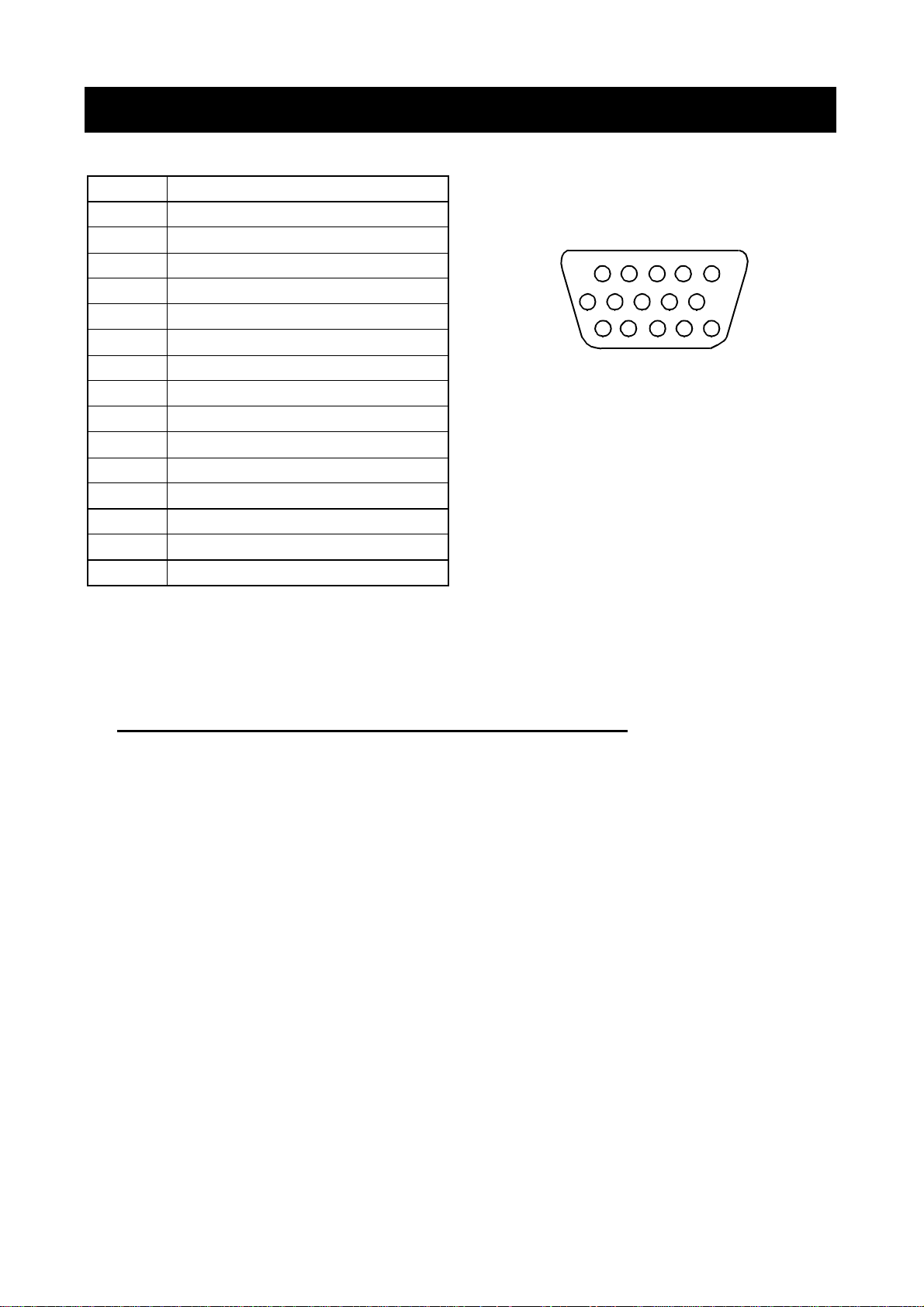
PIN CONNECTOR
Pin Signal
1 Red
2 Green
3 Blue
4 GND
5 GND
6 GND - Red
7 GND - Green
8 GND - Blue
9 +5Vdc
10 GND - H.Sync
11 GND - V.Sync
12 Bi-directional Data (SDA)
13 Horizontal Sync
14 Vertical Sync (VCLK)
15 Data clock (SCL)
1
6
Arrangement of 15-pin D-sub connector
10
15
u
CAUTION FOR ADJUSTMENT AND REPAIR
w The white balance adjustment has been done by a color analyzer in factroy. The adjustment proce-
dure, described in the service manual is made by a visual check.
w Allow 20 minutes warm-up time for the display before checking or adjusting only electrical specifica-
tion or function.
w Reform the leadwire after any repair work.
9
Page 11
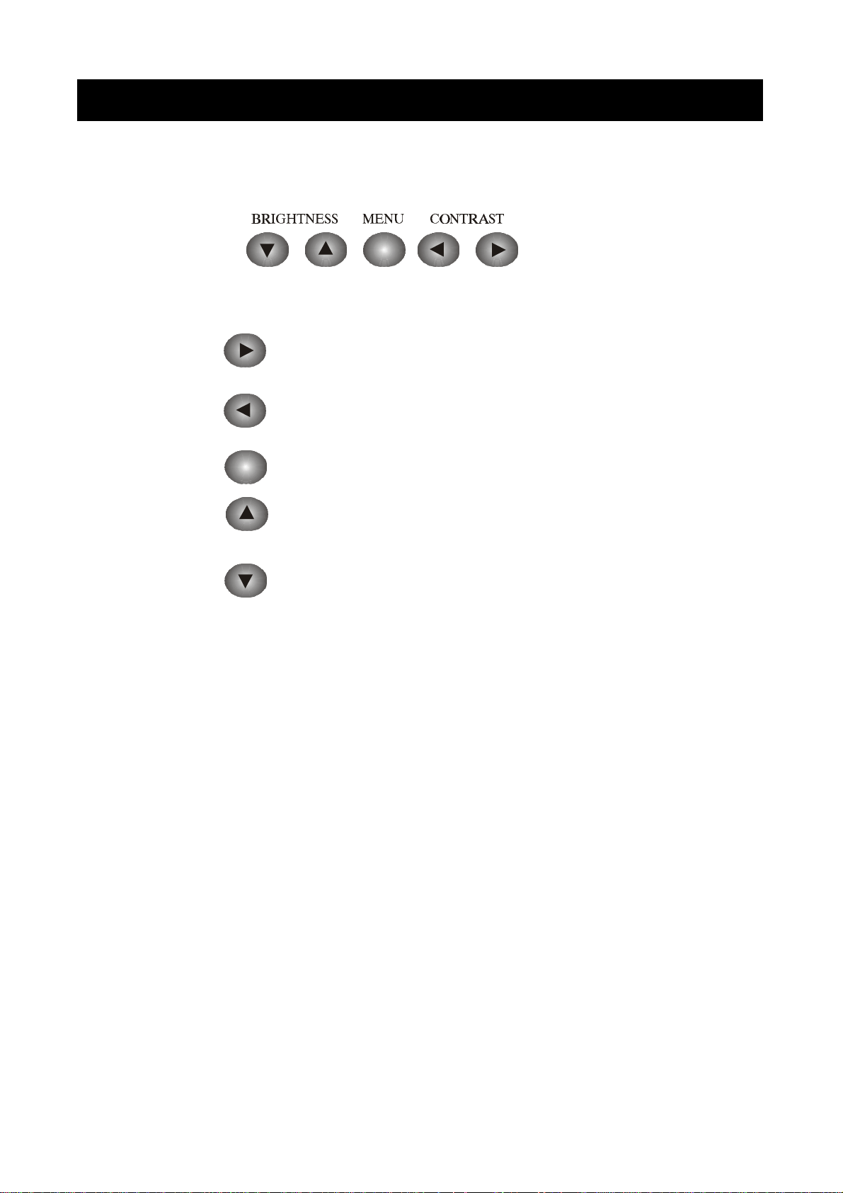
OPERATION & ADJUSTMENT
u
Control Panel
w Move cursor to the right window on the OSD window.
w Increase the value of any selected function.
w Move cursor to the left window on the OSD window.
w Decrease the value of any selected function.
w Launch OSD(On-Screen Display) MENU window.
w Move cursor to the high window on the OSD window.
w Increase the value of V.center.
w Move cursor to the low window on the OSD window.
w Decrease the value of V.center.
10
Page 12
u
R
G
B
Key Process
OPERATION & ADJUSTMENT
Start
w When you choose the icon on the OSD window, you can exit the OSD screen.
u
Hot Key
11
Page 13
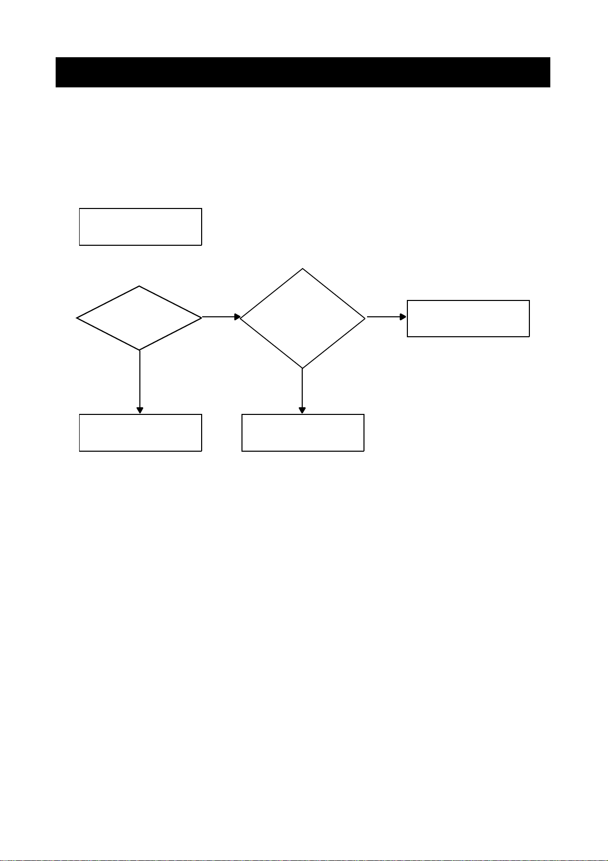
OPERATION & ADJUSTMENT
u
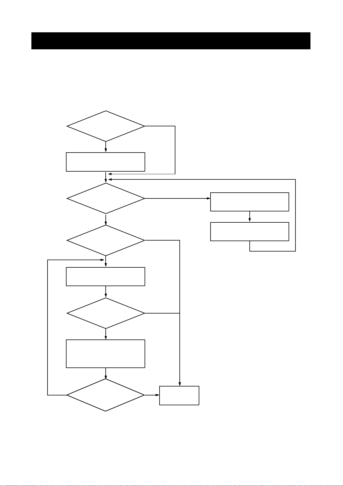
Adjustment procedure
Is the mode
1024x768?
Adjust the FIT SCREEN.
Is the H.Size
proper?
Is the
noise displayed on
the screen?
Perform the
AUTO TRACKING.
Yes
No
No
Adjust the control.
CLOCK
Perform the
AUTO POSITION.
Is the
noise displayed on
the screen?
Adjust the
CLOCK FINE
until the screen is cleared.
Is the
noise displayed on
the screen yet?
No
NoYes
End
12
Page 14
u
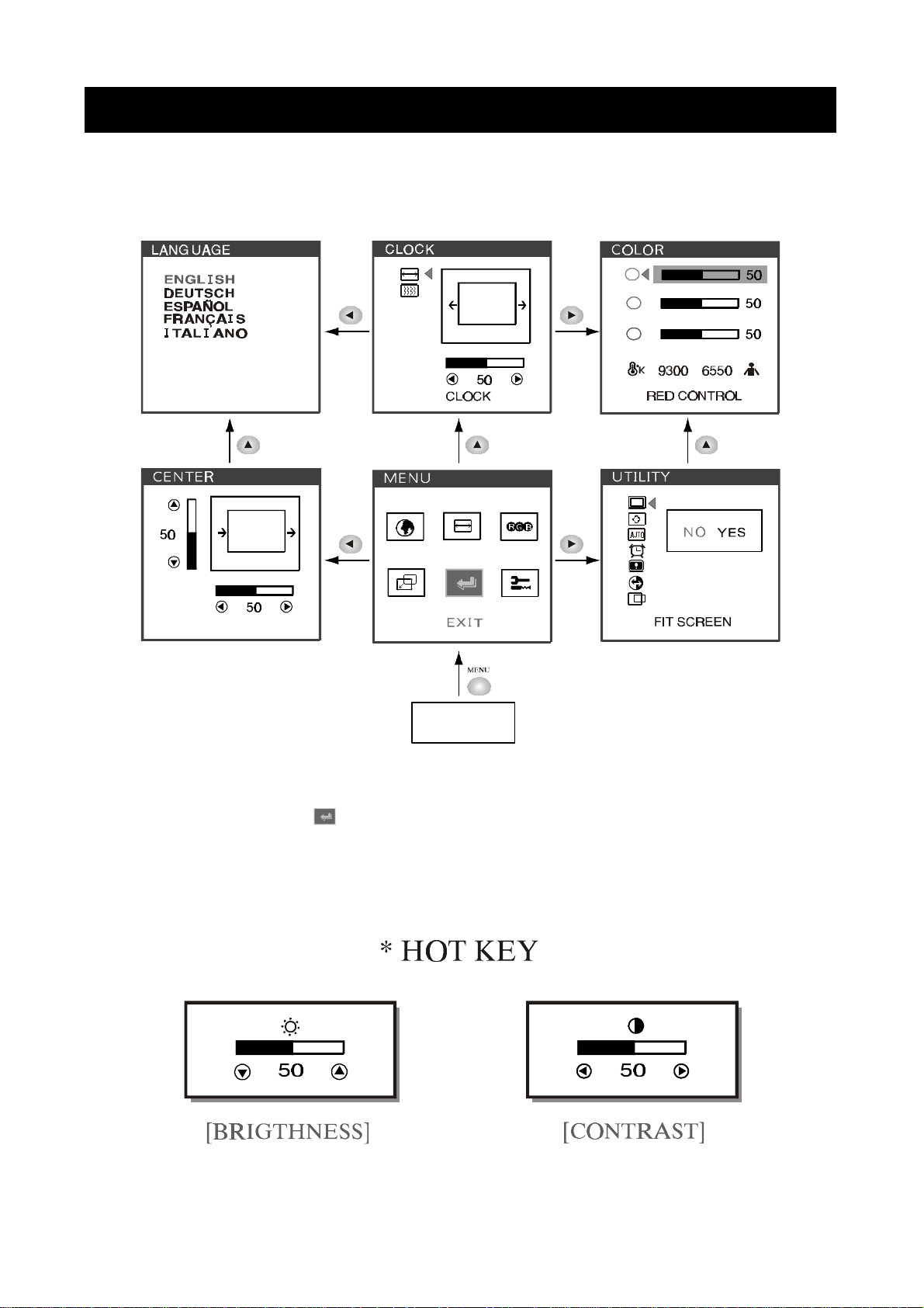
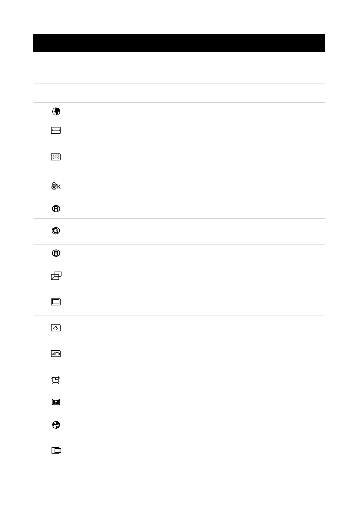
OSD Functions
ICON CONTROL FUNCTIONS
OPERATION & ADJUSTMENT
LANGUAGE
CLOCK
CLOCK FINE
COLOR TEMP
RED CONTROL
GREEN
CONTROL
BLUE CONTROL
H.CENTER &
V.CENTER
Select language for OSD (5 languages).
Adjust the width (horizontal size) of the screen image.
Sharpen the focus by aligning the illuminated pixels and adjust until the
screen image looks focused, crisp and sharp. Adjusting the CLOCK FINE
after the CLOCK adjustment will produce a clear screen.
Choose different preset color temperatures or set your own customized
color parameters.
Adjust the red color.
Adjust the green color.
Adjust the blue color.
Adjust the position of the display horizontally (left or right) and vertically
(up or down).
FIT SCREEN
SMART
SCALING
AUTO
TRACKING
OSD
TIME OUT
STATUS
RECALL
AUTO
POSITION
Make characters of displayed text easier to read (only for resolutions
lower than 1024x768).
Adjust the display image quality (if the screen proceed to scaling up).
Adjust the horizontal & vertical picture image quality and size.
Adjust the display OSD Menu.
Display horizontal & vertical frequency and polarity.
Reset the screen to the Factory Preset
Display Settings.
Choose automatically the proper horizontal position and vertical position
& size of the screen image.
13
Page 15

ALIGNMENT PROCEDURE
u
Standard Check point
1. Power source : 100-240Vac 50/60Hz
2. Aging: Take at least 20 minutes warm up time.
3. Signal
Video input :Analog 0.7Vpp 75Ω terminal positive polarity
Synchronizing : acceptable negative or positive at TTL level
Resolution
Horizontal : 1024 max.
Vertical : 768 max.
Frequency
Horizontal :30KHz - 62KHz
Vertical : 50Hz - 85Hz (available only non interlace mode)
u
Adjustment
1. Smart scaling set to 50%.
2. Contrast set to 100%.
3. Brightness set to 50%.
4. Switching to factory alignment mode
Press power key with down menu key( t ) at the power off status.
5. Video level adjustment
Receive stair pattern of 16 step (doesn’t care any mode).
Readjust coarse R, G, B in TDA8752 menu before saturation point.
6. Set up the tracking
See the user’s manual at page 8 th.
7. Switching to user’s mode
If turn-off and turn-on then switched to user’s mode.
* All of adjusted data stores by fade out of OSD.
14
Page 16

TROUBLE SHOOTING HINTS
1. Abnormal mode detect
Abnormal
mode detect
YES
Check input H. Sync
of TDA8752.
YES
Check
waveforms of #84 pin
of TDA8752
correct?
YES
Trouble in the
MX88281.
NO
NO
Trouble video input
circuit.
Trouble in the TDA8752.
15
Page 17

TROUBLESHOOTING HINTS
2. Trouble in Power on
Trouble in power on.
Power LED.
OFF
Check output
voltage of adapter.
YES
Is the 5VS line
normal?
YES
ON
NO
NO
Refer to No video
or No raster.
Trouble in adapter.
Trouble in SQ8 and its
ambient circuit.
Is the pulse of pin9
of the IC1?
YES
Trouble in IC2 or its
ambient circuit.
NO
Trouble in Q7 or its
ambient circuit.
16
Page 18

3. No raster
No raster.
Check the output
of the Q10 or #3 pin
of CN1.
< 2.5V
TROUBLESHOOTING HINTS
Trouble in the Q10 or
MX88281 (If it's trouble
in the MX88282, change
the main B'D)
> 2.5V
CN1 #1 pin
12V check.
YES
Check the DC/AC
output.
YES
Replace LCD panel.
NO
NO
Check the 12V of the
main power.
Trouble in DC/AC
inverter.
17
Page 19

TROUBLESHOOTING HINTS
4. One color is missing
One color is missing.
YES
Is OSD color
normal?
YES
Is input signal
normal?
YES
Are the R, G,
B digital (8 bit) output
of the U17
(TDA8752)?
NO
NO
NO
Check the output signal
of the MX88281
and 74act573.
Check video signal cable
or video card.
Replace the main B'D.
YES
Trouble in the
soldering.
18
Page 20

5. Pre check
Pre check
TROUBLESHOOTING HINTS
Check output
voltage
(5V/3.3V/12V).
YES
Trouble each trouble item.
NO
Check on/off
signal of micom.
YES
Check output
of Q9.
YES
Trouble in the SU1.
NO
NO
Check reset signal
(#9 pin of micom) and
its ambient circuit.
Trouble in the Q9 and
its ambient circuit.
19
Page 21
TROUBLESHOOTING HINTS
6. Abnormal video
Abnormal video
Is the OSD normal?
YES
Check the control and
data signal of SDRAM.
NO
Is LCLK output the
L1 waveform
normal?
YES
Check connection
of 41 pin cable.
NO
Check the output of
MX88281.
20
Page 22
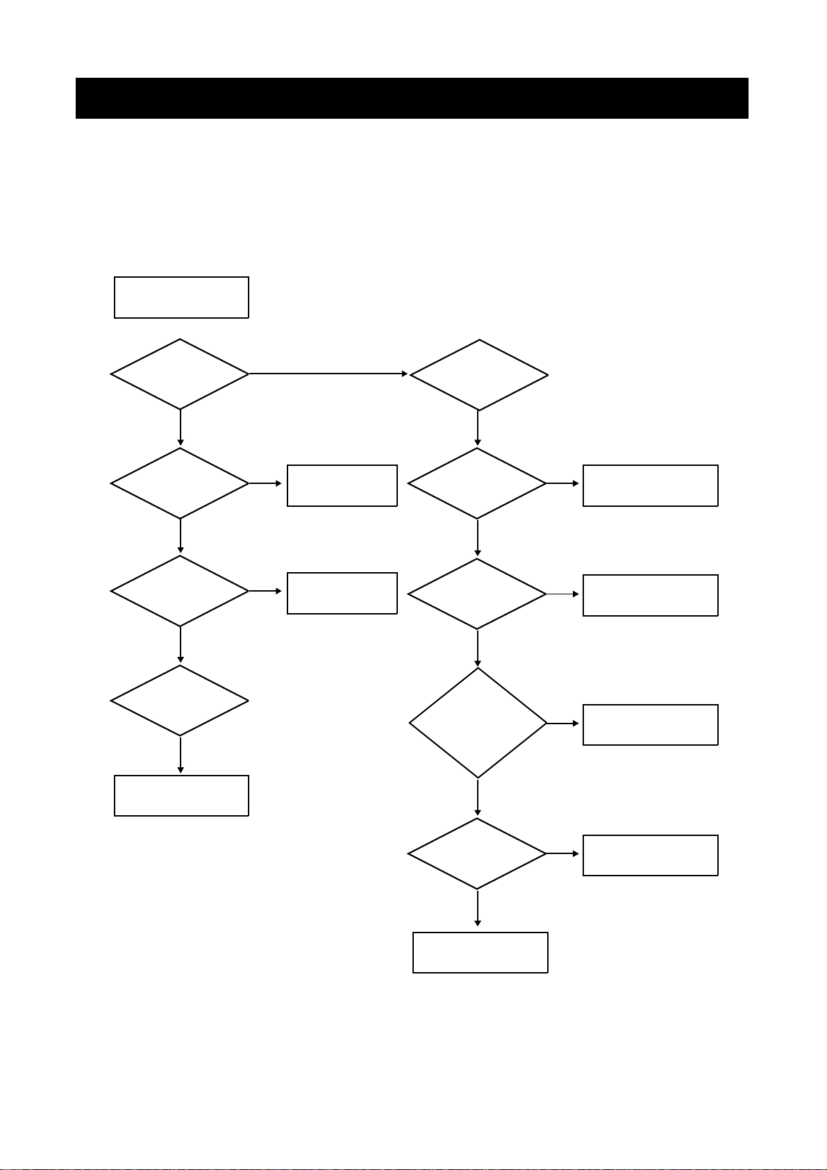
7. No video
No video
TROUBLESHOOTING HINTS
White
YES
OUT1 41 pin cable
connection check.
YES
U8 #2 pin
output 12V check?
YES
LVCC 3.3V check
YES
NO
NO
NO
Trouble connection.
Trouble connection.
Black
YES
Is OSD normal?
YES
Are the contrast
controls maximum?
YES
Are the video
signal and output signal
of the TDA8752?
NO
NO
NO
No raster
Change the contrast
control value to maximum
Change the main B'D
(Trouble in the TDA8752)
OK
YES
Are the output
signal of the MX88281?
YES
Check the LCD panel or
41 pin cable
21
NO
Change the main B'D
(Trouble in the TDA8752)
Page 23
BLOCK DIAGRAM
H,V sync &
dot clock
MX88281
10
16
Control line
Panel
Panel
driver
74ACT573
X 4
Buffer
Red
Green
Blue Blue
6
6
6
OSD
mixer
OSD signal
FRC
control &
dithering
Controller
Back
light
DC-AC
inverter
630VAC
62KHz
H,V sync &
pixel clock
OSD
circuit
Dimming control
DWOSD05
8
+12V
Address &
Data line
16M SDRAM X 3
KM416S1020CT X 3
10
Scaling
Dot clock
Address line
Red
Green 8
8
8
data line
+5V, +3.3V
& +12V out
Micom
I2C bus
( 78 E58 )
DC-DC converter &
On-off control
on-off control
Sampling
clock
TDA8752
RGB signal
From PC
15PIN DSUB
CONNECTOR
3
Offset & amplifier
PRE-AMP
Controller
3
ADC
Current &
resistance
PLL
V. sync
Clock timing
& phase
12V adapter
H. sync
H/V sync
2
74ACT14
Buffer
AC in
22
Page 24

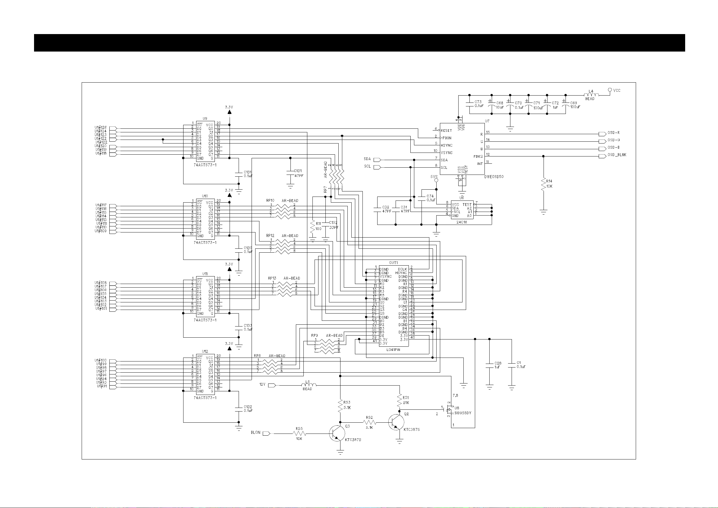
SCHEMATIC DIAGRAM
u
MAIN88281A
25
Page 25

SCHEMATIC DIAGRAM
u
TOP CIRCUIT
26
Page 26
u
BUFFER
SCHEMATIC DIAGRAM
27
Page 27
SCHEMATIC DIAGRAM
u
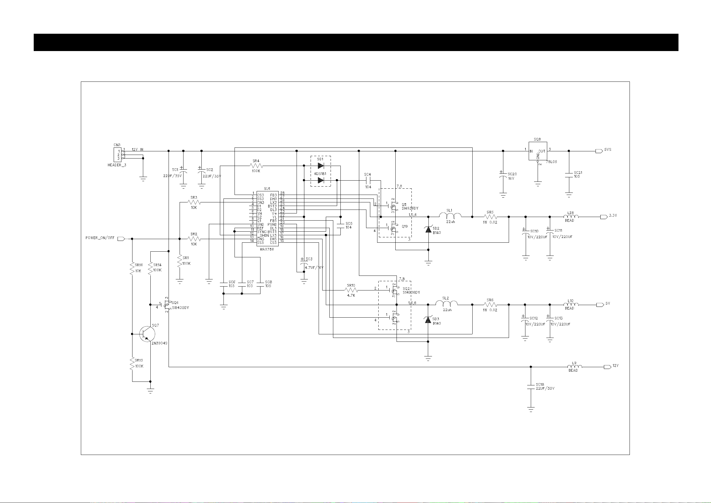
POWER DC/DC
28
Page 28

u
MEMORY
SCHEMATIC DIAGRAM
29
Page 29
SCHEMATIC DIAGRAM
u
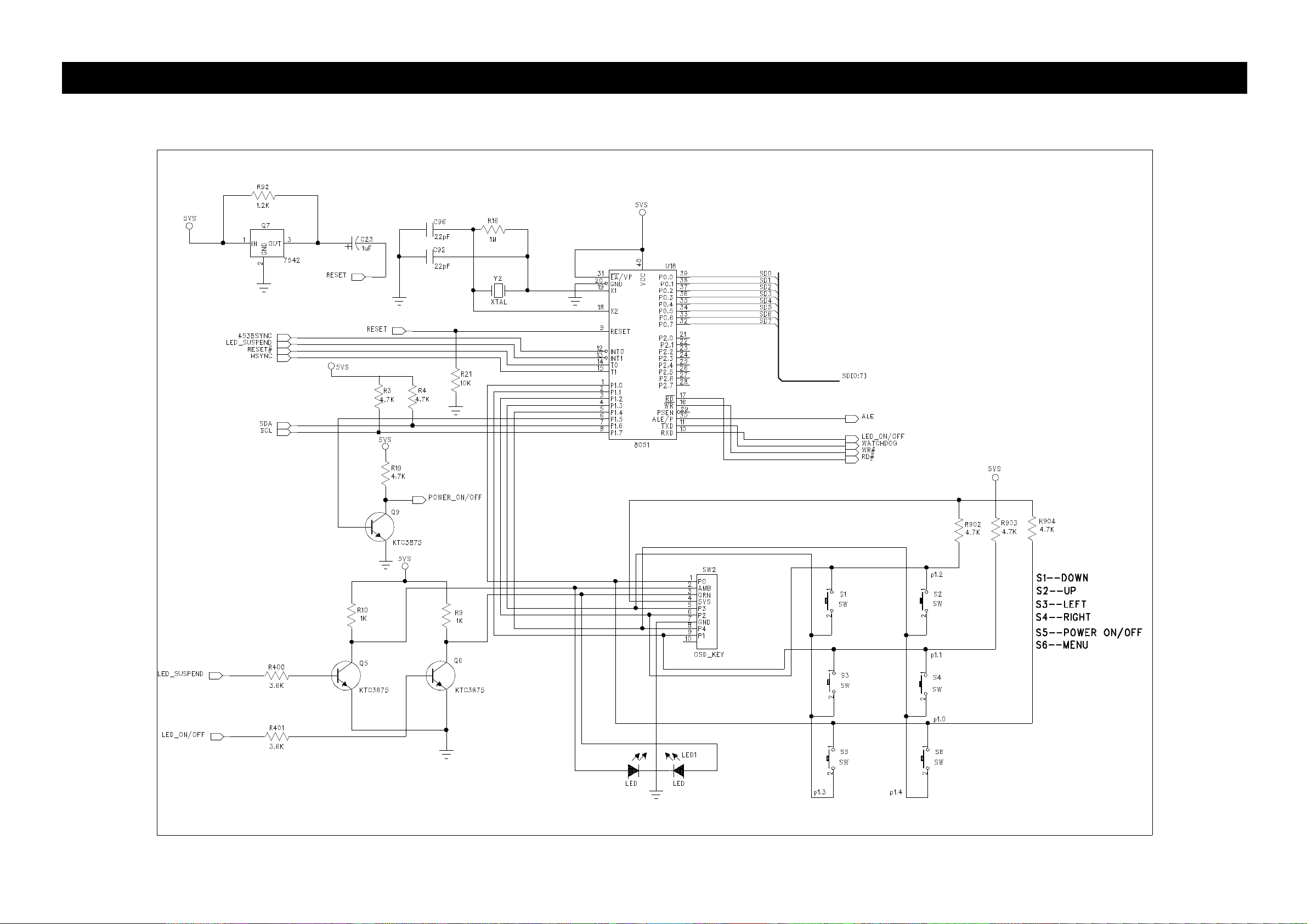
MICOM
30
Page 30

u
RGB/SYNC
SCHEMATIC DIAGRAM
31
Page 31

SCHEMATIC DIAGRAM
u
TDA8752A
32
Page 32
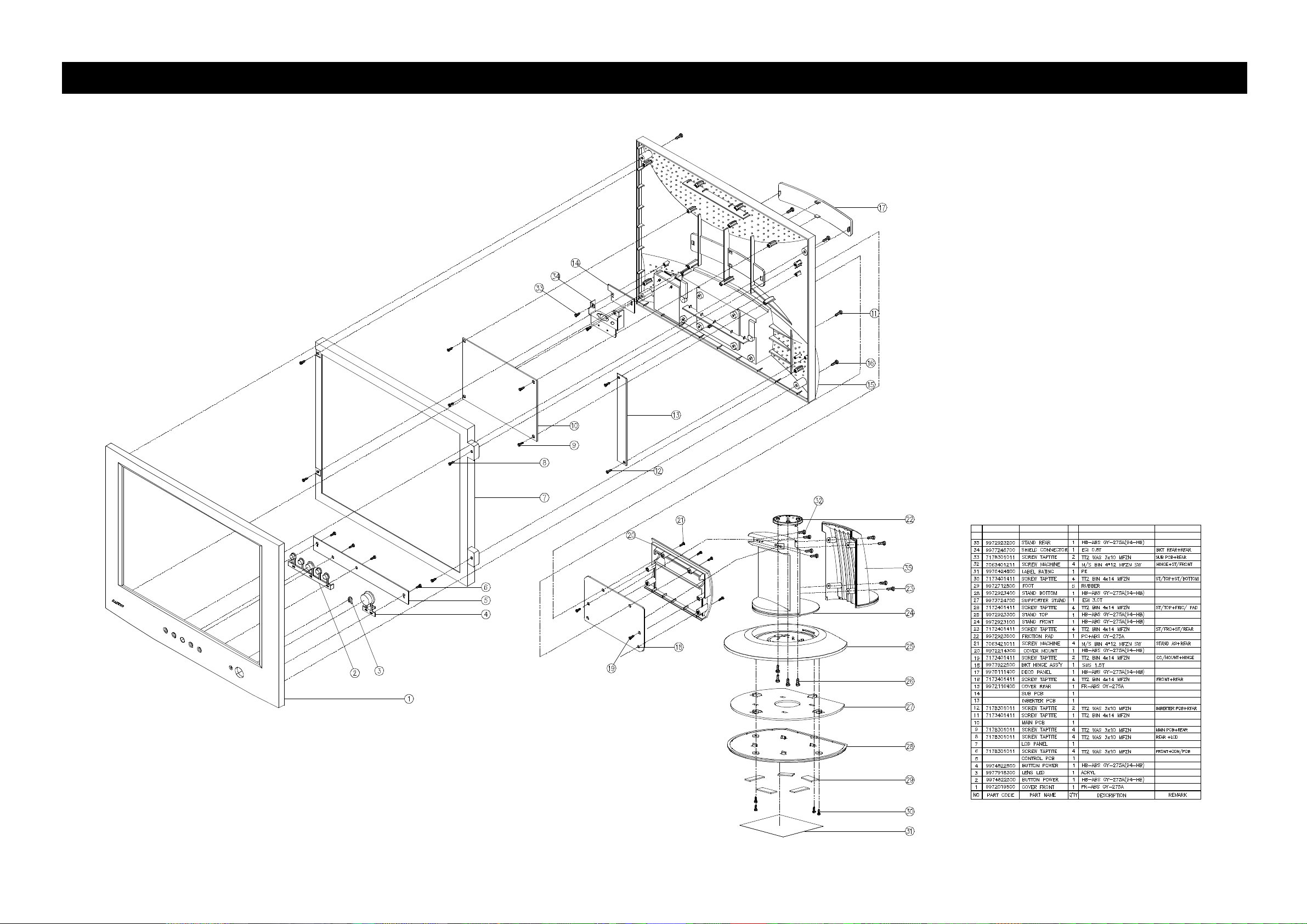
EXPLODED VIEW & MECHANICAL PARTS LIST
33
Page 33

INFORMATION OF PART DESCRIPTION
Important Safety Notice
Components identified with the International Symbol have special characteristics important for safety.
When replacing any components, use only manufacturer’s specified parts.
Abbreviation of Description
RESISTOR Description
Allowance
F
J
K
M
G
Example
Fig & Index Part No Description
R18
CAPACITOR Description
Allowance
C
D
F
±1%
±5%
±10%
±20%
±2%
Resistors
HRFT472JCA Chip=1/10W 472J
±0.25pF
±0.5%
±1pF
J
K
P
Z
Example
Fig & Index Part No Description
C044
±5%
±10%
±100% ~ 0%
±80% ~ -
HRFT104ZCA
Capacitors
Chip CERA 50V Y5V 0.1µF Z 2012
34
Page 34

ELECTRICAL PARTS LIST
The components identified by mark I have special characteristics important for safety and X-ray.
These should be replaced only with the types specified in the parts list.
LOC PART-CODE PART-NAME PART-DESC
AD1 9979720013 ADAPTER POWER ISA50-1
I
AD1A W3414M731- CORD POWER KKP-419C/KKS-15A 1.8M(BK)
C044 HCFK104ZCA C CHIP CERA 50V Y5V 0.1MF Z 2012
C045 HCFK104ZCA C CHIP CERA 50V Y5V 0.1MF Z 2012
C046 HCFK103ZCA C CHIP CERA 50V Y5V 0.01MF Z 2012
C047 HCFK103ZCA C CHIP CERA 50V Y5V 0.01MF Z 2012
C048 HCFK103ZCA C CHIP CERA 50V Y5V 0.01MF Z 2012
C049 HCFK104ZCA C CHIP CERA 50V Y5V 0.1MF Z 2012
C050 HCFK104ZCA C CHIP CERA 50V Y5V 0.1MF Z 2012
C051 HCFK104ZCA C CHIP CERA 50V Y5V 0.1MF Z 2012
C052 HCFK104ZCA C CHIP CERA 50V Y5V 0.1MF Z 2012
C053 HCFK104ZCA C CHIP CERA 50V Y5V 0.1MF Z 2012
C054 HCFK104ZCA C CHIP CERA 50V Y5V 0.1MF Z 2012
C055 HCFK104ZCA C CHIP CERA 50V Y5V 0.1MF Z 2012
C056 HCFK104ZCA C CHIP CERA 50V Y5V 0.1MF Z 2012
C057 HCFK104ZCA C CHIP CERA 50V Y5V 0.1MF Z 2012
C058 HCFK104ZCA C CHIP CERA 50V Y5V 0.1MF Z 2012
C059 HCFK104ZCA C CHIP CERA 50V Y5V 0.1MF Z 2012
C060 HCFK104ZCA C CHIP CERA 50V Y5V 0.1MF Z 2012
C061 HCFK104ZCA C CHIP CERA 50V Y5V 0.1MF Z 2012
C062 HCFK104ZCA C CHIP CERA 50V Y5V 0.1MF Z 2012
C063 HCFK104ZCA C CHIP CERA 50V Y5V 0.1MF Z 2012
C064 HCFK104ZCA C CHIP CERA 50V Y5V 0.1MF Z 2012
C065 HCFK104ZCA C CHIP CERA 50V Y5V 0.1MF Z 2012
C066 HCFK104ZCA C CHIP CERA 50V Y5V 0.1MF Z 2012
C067 HCQK220JCA C CHIP CERA 50V CH 22PF J 2012
C068 HCTAF109MB C CHIP TANTAL 16V 1MF M 3216
C069 HCTEF101MC C CHIP TANTAL 16V 100MF M 7343 TS
C070 HCFK104ZCA C CHIP CERA 50V Y5V 0.1MF Z 2012
C071 HCTEF101MC C CHIP TANTAL 16V 100MF M 7343 TS
C072 HCTAF109MB C CHIP TANTAL 16V 1MF M 3216
C073 HCFK104ZCA C CHIP CERA 50V Y5V 0.1MF Z 2012
C074 HCFK104ZCA C CHIP CERA 50V Y5V 0.1MF Z 2012
C075 HCQK102JCA C CHIP CERA 50V CH 1000PF J 2012
C076 HCTEJ220MC C CHIP TANTAL 35V 22MF M 7343
C077 HCFK104ZCA C CHIP CERA 50V Y5V 0.1MF Z 2012
C078 HCFK154ZCA C CHIP CERA Y5V 50V 0.15MF Z 2012
C079 HCFK104ZCA C CHIP CERA 50V Y5V 0.1MF Z 2012
C080 HCFK104ZCA C CHIP CERA 50V Y5V 0.1MF Z 2012
C081 HCFK104ZCA C CHIP CERA 50V Y5V 0.1MF Z 2012
LOC PART-CODE PART-NAME PART-DESC
C082 HCFK103ZCA C CHIP CERA 50V Y5V 0.01MF Z 2012
C083 HCFK103ZCA C CHIP CERA 50V Y5V 0.01MF Z 2012
C084 HCFK104ZCA C CHIP CERA 50V Y5V 0.1MF Z 2012
C085 HCFK104ZCA C CHIP CERA 50V Y5V 0.1MF Z 2012
C086 HCFK104ZCA C CHIP CERA 50V Y5V 0.1MF Z 2012
C087 HCFK223ZCA C CHIP CERA 50V Y5V 0.022MF Z 2012
C088 HCFK223ZCA C CHIP CERA 50V Y5V 0.022MF Z 2012
C090 HCTBF100MB C CHIP TANTAL 16V 10MF M 3528 TS
C091 HCFK104ZCA C CHIP CERA 50V Y5V 0.1MF Z 2012
C092 HCQK220JCA C CHIP CERA 50V CH 22PF J 2012
C093 HCFK104ZCA C CHIP CERA 50V Y5V 0.1MF Z 2012
C094 HCFK103ZCA C CHIP CERA 50V Y5V 0.01MF Z 2012
C095 HCFK103ZCA C CHIP CERA 50V Y5V 0.01MF Z 2012
C096 HCQK220JCA C CHIP CERA 50V CH 22PF J 2012
C097 HCFK103ZCA C CHIP CERA 50V Y5V 0.01MF Z 2012
C098 HCTBF100MB C CHIP TANTAL 16V 10MF M 3528 TS
C099 HCFK223ZCA C CHIP CERA 50V Y5V 0.022MF Z 2012
C1 HCFK104ZCA C CHIP CERA 50V Y5V 0.1MF Z 2012
C10 HCTBF100MB C CHIP TANTAL 16V 10MF M 3528 TS
C100 HCFK223ZCA C CHIP CERA 50V Y5V 0.022MF Z 2012
C101 HCFK223ZCA C CHIP CERA 50V Y5V 0.022MF Z 2012
C102 HCFK223ZCA C CHIP CERA 50V Y5V 0.022MF Z 2012
C103 HCQK102JCA C CHIP CERA 50V CH 1000PF J 2012
C104 HCFK104ZCA C CHIP CERA 50V Y5V 0.1MF Z 2012
C105 HCQK102JCA C CHIP CERA 50V CH 1000PF J 2012
C107 HCFK104ZCA C CHIP CERA 50V Y5V 0.1MF Z 2012
C108 HCFK104ZCA C CHIP CERA 50V Y5V 0.1MF Z 2012
C109 HCQK102JCA C CHIP CERA 50V CH 1000PF J 2012
C11 HCTBF100MB C CHIP TANTAL 16V 10MF M 3528 TS
C110 HCFK104ZCA C CHIP CERA 50V Y5V 0.1MF Z 2012
C111 HCTEF101MC C CHIP TANTAL 16V 100MF M 7343 TS
C112 HCQK102JCA C CHIP CERA 50V CH 1000PF J 2012
C113 HCQK102JCA C CHIP CERA 50V CH 1000PF J 2012
C114 HCQK102JCA C CHIP CERA 50V CH 1000PF J 2012
C115 HCTBF100MB C CHIP TANTAL 16V 10MF M 3528 TS
C116 HCQK102JCA C CHIP CERA 50V CH 1000PF J 2012
C117 HCFK474ZCA C CHIP CERA Y5V 50V 0.47MF Z 2012
C118 HCFK104ZCA C CHIP CERA 50V Y5V 0.1MF Z 2012
C119 HCQK102JCA C CHIP CERA 50V CH 1000PF J 2012
C12 HCFK104ZCA C CHIP CERA 50V Y5V 0.1MF Z 2012
35
Page 35

ELECTRICAL PARTS LIST
LOC PART-CODE PART-NAME PART-DESC
C120 HCFK474ZCA C CHIP CERA Y5V 50V 0.47MF Z 2012
C121 HCFK104ZCA C CHIP CERA 50V Y5V 0.1MF Z 2012
C122 HCFK104ZCA C CHIP CERA 50V Y5V 0.1MF Z 2012
C123 HCTBF100MB C CHIP TANTAL 16V 10MF M 3528 TS
C124 HCFF105ZEA C CHIP CERA 16V Y5V 1MF Z 3216
C125 HCQK121JCA C CHIP CERA 50V CH 120PF J 2012
C126 HCQK121JCA C CHIP CERA 50V CH 120PF J 2012
C127 HCTAF109MB C CHIP TANTAL 16V 1MF M 3216
C128 HCTBF100MB C CHIP TANTAL 16V 10MF M 3528 TS
C129 HCTBF100MB C CHIP TANTAL 16V 10MF M 3528 TS
C13 HCFK104ZCA C CHIP CERA 50V Y5V 0.1MF Z 2012
C130 HCFK104ZCA C CHIP CERA 50V Y5V 0.1MF Z 2012
C131 HCFK104ZCA C CHIP CERA 50V Y5V 0.1MF Z 2012
C132 HCFK104ZCA C CHIP CERA 50V Y5V 0.1MF Z 2012
C133 HCFK104ZCA C CHIP CERA 50V Y5V 0.1MF Z 2012
C136 HCTBF100MB C CHIP TANTAL 16V 10MF M 3528 TS
C139 HCTBF100MB C CHIP TANTAL 16V 10MF M 3528 TS
C14 HCTBF100MB C CHIP TANTAL 16V 10MF M 3528 TS
C141 HCFK104ZCA C CHIP CERA 50V Y5V 0.1MF Z 2012
C142 HCFK104ZCA C CHIP CERA 50V Y5V 0.1MF Z 2012
C143 HCFK104ZCA C CHIP CERA 50V Y5V 0.1MF Z 2012
C144 HCFK104ZCA C CHIP CERA 50V Y5V 0.1MF Z 2012
C145 HCFK104ZCA C CHIP CERA 50V Y5V 0.1MF Z 2012
C146 HCFK104ZCA C CHIP CERA 50V Y5V 0.1MF Z 2012
C147 HCFK104ZCA C CHIP CERA 50V Y5V 0.1MF Z 2012
C148 HCQK220JCA C CHIP CERA 50V CH 22PF J 2012
C149 HCQK220JCA C CHIP CERA 50V CH 22PF J 2012
C15 HCTBF100MB C CHIP TANTAL 16V 10MF M 3528 TS
C150 HCFK104ZCA C CHIP CERA 50V Y5V 0.1MF Z 2012
C151 HCQK470JCA C CHIP CERA 50V CH 47PF J 2012
C152 HCQK330JCA C CHIP CERA 50V CH 33PF J 2012
C16 HCTBF100MB C CHIP TANTAL 16V 10MF M 3528 TS
C17 HCTBF100MB C CHIP TANTAL 16V 10MF M 3528 TS
C179 HCTEF101MC C CHIP TANTAL 16V 100MF M 7343 TS
C18 HCFK104ZCA C CHIP CERA 50V Y5V 0.1MF Z 2012
C19 HCFK104ZCA C CHIP CERA 50V Y5V 0.1MF Z 2012
C2 HCQK220JCA C CHIP CERA 50V CH 22PF J 2012
C20 HCTBF100MB C CHIP TANTAL 16V 10MF M 3528 TS
C21 HCFK104ZCA C CHIP CERA 50V Y5V 0.1MF Z 2012
C22 HCFK104ZCA C CHIP CERA 50V Y5V 0.1MF Z 2012
C23 HCTAF109MB C CHIP TANTAL 16V 1MF M 3216
C24 HCFK104ZCA C CHIP CERA 50V Y5V 0.1MF Z 2012
C25 HCFK104ZCA C CHIP CERA 50V Y5V 0.1MF Z 2012
C27 HCFK104ZCA C CHIP CERA 50V Y5V 0.1MF Z 2012
LOC PART-CODE PART-NAME PART-DESC
C273 HCQK102JCA C CHIP CERA 50V CH 1000PF J 2012
C28 HCTBF100MB C CHIP TANTAL 16V 10MF M 3528 TS
C29 HCTBF100MB C CHIP TANTAL 16V 10MF M 3528 TS
C3 HCQK220JCA C CHIP CERA 50V CH 22PF J 2012
C31 HCQK470JCA C CHIP CERA 50V CH 47PF J 2012
C32 HCQK470JCA C CHIP CERA 50V CH 47PF J 2012
C33 HCTBF100MB C CHIP TANTAL 16V 10MF M 3528 TS
C34 HCQK150JCA C CHIP CERA 50V CH 15PF J 2012
C35 HCTBF100MB C CHIP TANTAL 16V 10MF M 3528 TS
C36 HCTBF100MB C CHIP TANTAL 16V 10MF M 3528 TS
C37 HCFK104ZCA C CHIP CERA 50V Y5V 0.1MF Z 2012
C38 HCFK474ZCA C CHIP CERA Y5V 50V 0.47MF Z 2012
C39 HCFK474ZCA C CHIP CERA Y5V 50V 0.47MF Z 2012
C4 HCFK104ZCA C CHIP CERA 50V Y5V 0.1MF Z 2012
C40 HCTBF100MB C CHIP TANTAL 16V 10MF M 3528 TS
C41 HCTBF100MB C CHIP TANTAL 16V 10MF M 3528 TS
C42 HCTBF100MB C CHIP TANTAL 16V 10MF M 3528 TS
C43 HCTBF100MB C CHIP TANTAL 16V 10MF M 3528 TS
C5 HCFK104ZCA C CHIP CERA 50V Y5V 0.1MF Z 2012
C6 HCQK100JCA C CHIP CERA 50V CH 10PF Z 2012
C7 HCFK104ZCA C CHIP CERA 50V Y5V 0.1MF Z 2012
C8 HCFK104ZCA C CHIP CERA 50V Y5V 0.1MF Z 2012
C813 HCQK102JCA C CHIP CERA 50V CH 1000PF J 2012
C9 HCFK104ZCA C CHIP CERA 50V Y5V 0.1MF Z 2012
CA01 9970800035 CABLE SIGNAL AS 15P+15P/DDC=1.5M(GY275A)
CN1 9979220020 CONN WAFER SMAW250-05 (ANGLE)
CN1A 9970750034 CONN AS SMH250+5264-5+1007#24=110
CN2 9979220024 CONN WAFER SMAW250-09 (ANGLE)
CN2A 9970790107 CONN AS SMH250-9*2+1007#24=270
CN3 9979220018 CONN WAFER SMAW250-03 (ANGLE)
CN3A 9970730071 CONN AS SMH250-3*2+1354#28=250
CN4 9979220021 CONN WAFER SMAW250-06 (ANGLE)
CN4A 9970760042 CONN AS SMH250-6*2+2464#24=120
CN5 9979220022 CONN WAFER SMAW250-07 (ANGLE)
CN5A 9970760043 CONN AS SMH250+1354#28+OP14A=100
CW1 9979220022 CONN WAFER SMAW250-07 (ANGLE)
CW2 9979220021 CONN WAFER SMAW250-06 (ANGLE)
CW3 9979220018 CONN WAFER SMAW250-03 (ANGLE)
CW4 9979220024 CONN WAFER SMAW250-09 (ANGLE)
D1 DRLS4148-- DIODE CHIP RLS4148
D2 DRLS4148-- DIODE CHIP RLS4148
D3 DRLS4148-- DIODE CHIP RLS4148
D4 DRLS4148-- DIODE CHIP RLS4148
D5 DRLZ5R6B-B DIODE ZENER CHIP RLZTE-11 5.6B
36
Page 36

ELECTRICAL PARTS LIST
LOC PART-CODE PART-NAME PART-DESC
DSUB1
9979200209 D-SUB 15P ANGLE 15P DDC BLUE W/IN SCREW
EF1 5PF1BH471M FILTER LC CFI-06-B-1H-471M
IC1 1DWM300--- IC MICOM W78E58-24
IC1A 9979300500 SOCKET IC WSDIF-40T
IC2 174HCT4538 IC 74HCT4538D
I
INV1 DBA11501-- LCD INVERTER BAI1501
J001 85801052GY WIRE COPPER 1/0.52 TIN COATING
J002 85801052GY WIRE COPPER 1/0.52 TIN COATING
J003 85801052GY WIRE COPPER 1/0.52 TIN COATING
J004 85801052GY WIRE COPPER 1/0.52 TIN COATING
J005 85801052GY WIRE COPPER 1/0.52 TIN COATING
J006 85801052GY WIRE COPPER 1/0.52 TIN COATING
J007 85801052GY WIRE COPPER 1/0.52 TIN COATING
J008 85801052GY WIRE COPPER 1/0.52 TIN COATING
J009 85801052GY WIRE COPPER 1/0.52 TIN COATING
J010 85801052GY WIRE COPPER 1/0.52 TIN COATING
J011 85801052GY WIRE COPPER 1/0.52 TIN COATING
JACK1 9979100010 JACK DC POWER JACK 6.5PIE 14.5*9
L1 HFFTB2601B COIL CHIP BEAD TB321611Z260
L10 HFFTB2601B COIL CHIP BEAD TB321611Z260
L11 HFFTB2601B COIL CHIP BEAD TB321611Z260
L12 HFFTB2601B COIL CHIP BEAD TB321611Z260
L13 HFFTB2601B COIL CHIP BEAD TB321611Z260
L15 HFFTB2601B COIL CHIP BEAD TB321611Z260
L16 HFFTB2601B COIL CHIP BEAD TB321611Z260
L2 HFFTB2601B COIL CHIP BEAD TB321611Z260
L28 HFFTB2601B COIL CHIP BEAD TB321611Z260
L4 HFFTB2601B COIL CHIP BEAD TB321611Z260
L5 HFFTB2601B COIL CHIP BEAD TB321611Z260
L6 HFFTB2601B COIL CHIP BEAD TB321611Z260
L7 HFFTB2601B COIL CHIP BEAD TB321611Z260
L8 HFFTB2601B COIL CHIP BEAD TB321611Z260
L9 HFFTB2601B COIL CHIP BEAD TB321611Z260
LCD DLM151X2C2 LCD LM151X2-C2TH
LED1 DSD50GYW-- LED SD50GYW(GREEN/AMBER)
OUT1 9979220080 CONN WAFER DBBV-41PJ-1.0SM
OUTA 9970741001 CONN AS DF-9-41S*2+1571#32=220
Q10 TKTC3875SY TR CHIP KTC3875SY(RTK)
Q12 DKDS226RTK DIODE CHIP KDS226(RTK)
Q13 DKDS226RTK DIODE CHIP KDS226(RTK)
Q14 DKDS226RTK DIODE CHIP KDS226(RTK)
Q15 DKDS226RTK DIODE CHIP KDS226(RTK)
Q16 DKDS226RTK DIODE CHIP KDS226(RTK)
Q17 DKDS226RTK DIODE CHIP KDS226(RTK)
LOC PART-CODE PART-NAME PART-DESC
Q2 TKTC3875SY TR CHIP KTC3875SY(RTK)
Q3 TKTC3875SY TR CHIP KTC3875SY(RTK)
Q4 1K1A7805P1 IC REGULATOR KIA7805API
Q5 TKTC3875SY TR CHIP KTC3875SY(RTK)
Q6 TKTC3875SY TR CHIP KTC3875SY(RTK)
Q7 1KA7542--- IC VOTAGE DETECTOR KA7542
Q8 DKDS226RTK DIODE CHIP KDS226(RTK)
Q9 TKTC3875SY TR CHIP KTC3875SY(RTK)
R001 RD-AZ472J- R CARBON FILM 1/6 4.7K OHM J
R002 RD-AZ472J- R CARBON FILM 1/6 4.7K OHM J
R003 RD-AZ472J- R CARBON FILM 1/6 4.7K OHM J
R1 HRFT472JCA R CHIP 1/10 4.7K OHM J 2012
R10 HRFT102JCA R CHIP 1/10 1K OHM J 2012
R11 HRFT101JCA R CHIP 1/10 100 OHM J 2012
R12 HRFT104JCA R CHIP 1/10 100K OHM J 2012
R13 HRFT474JCA R CHIP 1/10 470K OHM J 2012
R14 HRFT103JCA R CHIP 1/10 10K OHM J 2012
R15 RD-2Z101J- R CARBON FILM 1/2 100 OHM J
R16 HRFT105JCA R CHIP 1/10 1M OHM J 2012
R17 HRFT105JCA R CHIP 1/10 1M OHM J 2012
R18 HRFT472JCA R CHIP 1/10 4.7K OHM J 2012
R19 HRFT472JCA R CHIP 1/10 4.7K OHM J 2012
R2 HRFT220JCA R CHIP 1/10 22 OHM J 2012
R20 HRFT472JCA R CHIP 1/10 4.7K OHM J 2012
R22 HRFT472JCA R CHIP 1/10 4.7K OHM J 2012
R23 HRFT473JCA R CHIP 1/10 47K OHM J 2012
R3 HRFT472JCA R CHIP 1/10 4.7K OHM J 2012
R32 HRFT000JCA R CHIP 1/10 0 OHM J 2012
R34 HRFT220JCA R CHIP 1/10 22 OHM J 2012
R35 HRFT220JCA R CHIP 1/10 22 OHM J 2012
R36 HRFT102JCA R CHIP 1/10 1K OHM J 2012
R4 HRFT472JCA R CHIP 1/10 4.7K OHM J 2012
R40 HRFT472JCA R CHIP 1/10 4.7K OHM J 2012
R400 HRFT362JCA R CHIP 1/10 3.6K OHM J 2012
R401 HRFT362JCA R CHIP 1/10 3.6K OHM J 2012
R41 HRFT472JCA R CHIP 1/10 4.7K OHM J 2012
R5 HRFT220JCA R CHIP 1/10 22 OHM J 2012
R51 HRFT513JCA R CHIP 1/10 51K OHM J 2012
R52 HRFT512JCA R CHIP 1/10 5.1K OHM J 2012
R53 HRFT512JCA R CHIP 1/10 5.1K OHM J 2012
R55 HRFT103JCA R CHIP 1/10 10K OHM J 2012
R6 HRFT472JCA R CHIP 1/10 4.7K OHM J 2012
R7 HRFT101JCA R CHIP 1/10 100 OHM J 2012
R8 HRFT472JCA R CHIP 1/10 4.7K OHM J 2012
37
Page 37

ELECTRICAL PARTS LIST
LOC PART-CODE PART-NAME PART-DESC
R801 HRFT750JCA R CHIP 1/10 75 OHM J 2012
R811 HRFT750JCA R CHIP 1/10 75 OHM J 2012
R821 HRFT750JCA R CHIP 1/10 75 OHM J 2012
R9 HRFT102JCA R CHIP 1/10 1K OHM J 2012
R92 HRFT302JCA R CHIP 1/10 3K OHM J 2012
RP1 HFFH4H300E COIL CHIP BEAD HB-4H3216-300JT
RP10 HFFH4M121E COIL CHIP BEAD HB-4M3216-121JT
RP12 HFFH4M121E COIL CHIP BEAD HB-4M3216-121JT
RP13 HFFH4M121E COIL CHIP BEAD HB-4M3216-121JT
RP2 HFFH4H300E COIL CHIP BEAD HB-4H3216-300JT
RP3 HFFH4H300E COIL CHIP BEAD HB-4H3216-300JT
RP4 HFFH4H300E COIL CHIP BEAD HB-4H3216-300JT
RP5 HFFH4H300E COIL CHIP BEAD HB-4H3216-300JT
RP7 HFFH4M121E COIL CHIP BEAD HB-4M3216-121JT
RP8 HFFH4M121E COIL CHIP BEAD HB-4M3216-121JT
RP9 HFFH4M121E COIL CHIP BEAD HB-4M3216-121JT
RW2 RS01Z330J- R M-OXIDE FILM 1W 33 OHM J (TAPPING)
S001 5S50101Z01 SW TACT KPT-1115VM 1C-1P
S002 5S50101Z01 SW TACT KPT-1115VM 1C-1P
S003 5S50101Z01 SW TACT KPT-1115VM 1C-1P
S004 5S50101Z01 SW TACT KPT-1115VM 1C-1P
S005 5S50101Z01 SW TACT KPT-1115VM 1C-1P
S006 5S50101Z01 SW TACT KPT-1115VM 1C-1P
SC1 HCTEJ220MC C CHIP TANTAL 35V 22MF M 7343
SC10 HCTED221MC C CHIP TANTAL 10V 220MF M 7343
SC11 HCTED221MC C CHIP TANTAL 10V 220MF M 7343
SC12 HCTED221MC C CHIP TANTAL 10V 220MF M 7343
SC13 HCTED221MC C CHIP TANTAL 10V 220MF M 7343
SC18 HCTEJ220MC C CHIP TANTAL 35V 22MF M 7343
SC2 HCTEJ220MC C CHIP TANTAL 35V 22MF M 7343
SC20 HCTBF100MB C CHIP TANTAL 16V 10MF M 3528 TS
SC21 HCFF105ZEA C CHIP CERA 16V Y5V 1MF Z 3216
SC3 HCTBF479MB C CHIP TANTAL 16V 4.7MF M 3528
SC4 HCFK104ZCA C CHIP CERA 50V Y5V 0.1MF Z 2012
SC5 HCFK104ZCA C CHIP CERA 50V Y5V 0.1MF Z 2012
SC6 HCFK103ZCA C CHIP CERA 50V Y5V 0.01MF Z 2012
SC7 HCFK103ZCA C CHIP CERA 50V Y5V 0.01MF Z 2012
SC8 HCFF105ZEA C CHIP CERA 16V Y5V 1MF Z 3216
SD1 DKDS181RTK DIODE CHIP KDS181(RTK)
LOC PART-CODE PART-NAME PART-DESC
SD2 DSK14----- DIODE SCHOTTKY SK14
SD3 DSK14----- DIODE SCHOTTKY SK14
SL1 HLC220M00E L CHIP COIL 22UH M (BA220)
SL2 HLC220M00E L CHIP COIL 22UH M (BA220)
SQ1 TFDS6930A- FET CHIP FDS6930A
SQ2 TFDS6930A- FET CHIP FDS6930A
SQ3 1K1A78L05F IC REGULATOR CHIP KIA78L05F(RTF)
SQ6 TNDS9435A- FET CHIP NDS9435A
SQ7 T2N3904SRT TR CHIP 2N3904S(RTK)
SQ8 1K1A78L05F IC REGULATOR CHIP KIA78L05F(RTF)
SR1 HRFT104JCA R CHIP 1/10 100K OHM J 2012
SR10 HRFT220JCA R CHIP 1/10 22 OHM J 2012
SR14 HRFT104JCA R CHIP 1/10 100K OHM J 2012
SR15 HRFT104JCA R CHIP 1/10 100K OHM J 2012
SR16 HRFT113JCA R CHIP 1/10 11K OHM J 2012
SR2 HRFT103JCA R CHIP 1/10 10K OHM J 2012
SR3 HRFT103JCA R CHIP 1/10 10K OHM J 2012
SR4 HRFT104JCA R CHIP 1/10 100K OHM J 2012
SR5 HRM1407JPD R CHIP METAL PLATE 1W 0.04 OHM J 8340
SR6 HRM1207JPD R CHIP METAL PLATE 1W 0.02 OHM J 8340
SU1 1SB3052P-- IC SB3052P(SSOP-28)
U015 1M62393P-- IC DAC M62393P
U017 1TDA8752AH IC ADC TDA8752AH/8
U019 1TC74ACT14 IC TC74ACT14FN
U1 1MX88281FC IC LCD CONTROLLER MX88281FC
U10 1TC74ACT57 IC TC74ACT573FT(EL)
U11 1TC74ACT57 IC TC74ACT573FT(EL)
U12 1TC74ACT57 IC TC74ACT573FT(EL)
U16 1AT24C21-- IC EEPROM AT24C21
U2 1ZRC250N80 IC ZRC250N802
U3 1KM416S102 IC SDRAM KM416S1020CT-G8
U4 1KM416S102 IC SDRAM KM416S1020CT-G8
U5 1KM416S102 IC SDRAM KM416S1020CT-G8
U6 1AT24C1610 IC AT24C16-10PC
U7 1DW0SD05-- IC OSD DWOSD05
U8 TNDS9958-- FET CHIP NDS9958
U9 1TC74ACT57 IC TC74ACT573FT(EL)
Y1 5XJ14R318F CRYSTAL QUARTZ HC-49/S 14.31818MHZ 50PPM
Y2 5XJ11R059E CRYSTAL HC-49/S 11.0592MHZ 30PPM
38
 Loading...