

Page 1

S/M No. : VS123MUEF1
Service Manual
Video Cassette Recorder
Multi Models(S2-MECHA)
Model:PAL/MESECAM/NTSC
(DV-S123W Series)
(DV-S103W Series)
PAL-N/NTSC
(DV-S123A Series)
(DV-S103A Series)
NTSC Only Models
(DV-S123N Series)
(DV-S103N Series)
DAEWOO ELECTRONICS CO., LTD.
URL : http://svc.dwe.co.kr
Page 2

TABLE OF CONTENTS
SAFETY&PRECAUTIONS ............................................................................................... 2
EXTERNAL VIEWS ........................................................................................................ 4
1. FRONT VIEWS FUNCTION ............................................................................................................... 4
2. REAR VIEWS FUNCTION ................................................................................................................. 5
GENERAL ADJUSTMENT .............................................................................................. 6
SPECIFICATIONS ....................................................................................................... 7
TROUBLE SHOOTING GUIDE ........................................................................................ 8
1. TROUBLE SHOOTING FLOW CHART ................................................................................................ 8
2. VOLTAGE CHART ........................................................................................................................... 25
3. WAVEFORMS ON VIDEO CIRCUIT .................................................................................................. 26
4.¥ì-COM PIN ASSIGNMENT ........................................................................................................... 29
PRINTED CIRCUIT BOARD ............................................................................................ 32
1. PCB MAIN ..................................................................................................................................... 32
2. PCB POWER(SMPS) ........................................................................................................................ 33
CIRCUIT DIAGRAM ..................................................................................................... 34
1. CONNECTION DIAGRAM .............................................................................................................. 34
2. POWER CIRCUIT ............................................................................................................................ 35
3. SERVO SYSCON CIRCUIT ............................................................................................................... 36
4. AV INPUT OUTPUT CIRCUIT .............................................................................................................. 37
5. VIDEO AUDIO CIRCUIT .................................................................................................................. 38
EXPLODING VIEWS & PARTS LIST ................................................................................. 39
1. PACKING AS ................................................................................................................................. 39
2. SET TOTAL ASSEMBLY ..................................................................................................................... 40
3. FRONT PANEL ASSEMBLY ............................................................................................................... 41
ELECTRICAL PARTS LIST ............................................................................................... 43
1. PCB MAIN AS ................................................................................................................................ 43
2. PCB AUTO VOLT REGULATOR AS ................................................................................................. 48
3. DIFFERNCE PARTS LIST ................................................................................................................... 49
1
Page 3
SAFETY&PRECAUTIONS
SAFETY CHECK AFTER SERVING
Examine the area surrounding the repaired location for damage or deterioration. Observe that screw, parts and wires
have been returned to original positions. Afterwards, perform the following tests and conform the specified values in order
to verify compliance whit safety standards.
1. Insulation resistance test
Confirm the specified insulation resistance between power cord plug prong and externally exposed parts of the set
(RF terminals, antenna terminals, video and audio input and output terminals, microphone jacks, earphone jacks, etc.)
is
greater than values given in table 1 below.
2. Dielectric strengthen test
Confirm specified dielectric strengthen between power
cord plug prongs and exposed accessible parts of the set
(RF terminals, antenna terminals, video and audio input
output terminals, microphone jack, ear phone jacks, etc.)
is greater than values given table 1.
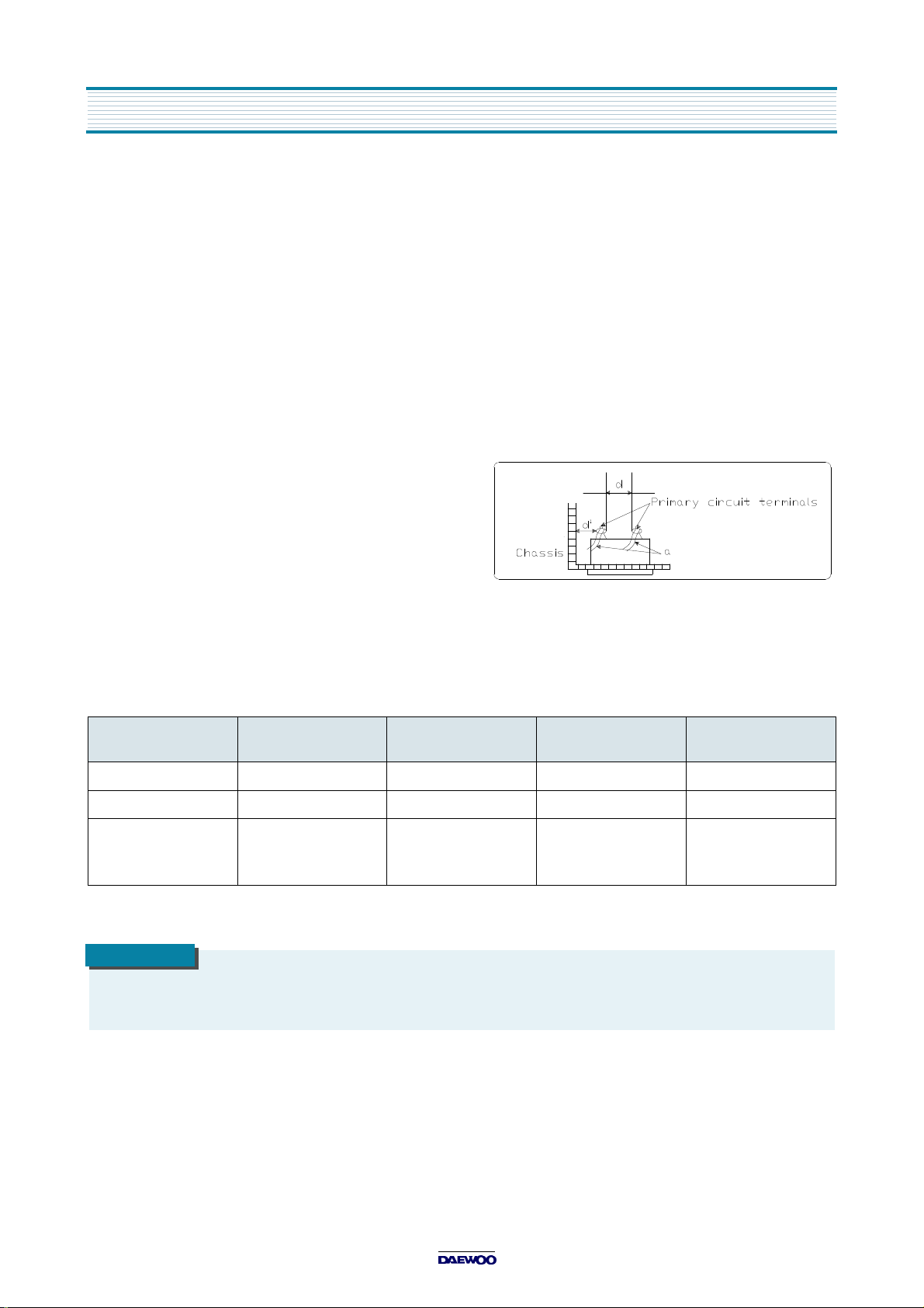
3. Clearance distance
When replacing primary circuit component, confirm specified clearance distance (d), (d’) between soldered terminals,
and between terminals and surrounding metallic parts. See table below.
Rating for selected areas
AC Line Voltage Region
100V Japan
110 to 130V
* 110 to 130V
200 to 240V
* : Class model only
USA & Canada
Latin America
Europe
Australia
Insulation
Resistance
¡Ã1§Û
/500V DC 1
- 900V AC 1min.
¡Ã10§Û
/500V DC 4§Ç AC 1min.
Dielectric
Strength
§Ç
AC 1min.
Clearance
Distance(d),(d)
¡Ã
3
¡Ã
3.2
¡Ã
6(d)
¡Ã
8(d’)
(a :Power cord)
NOTE
This table is unofficial and for reference only. Be sure to confirm the precise values for your
particular country and locality
2
Page 4
SAFETY&PRECAUTIONS
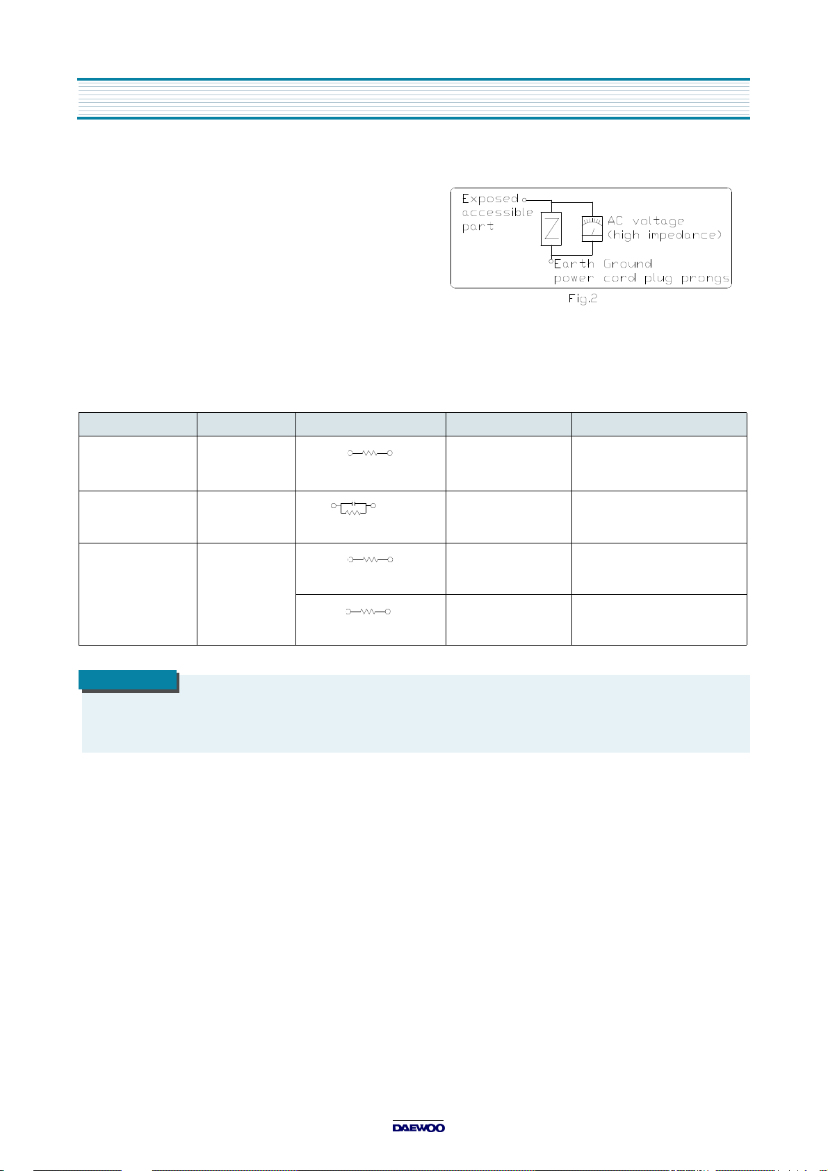
4. Leakage current test
Confirm specified or lower leakage current between
B(earth ground, power cord plug prongs) and externally
exposed accessible parts (RF terminals, antenna terminals, video and audio input output terminals, microphone
jacks, earphone jacks, etc.)
Measuring method:(Power ON) Insert load Z between
B(earth ground, power cord plug prongs) and exposed
accessible parts. Use on AC voltmeter to measure across
both terminals of load Z. See figure2 and following table.
Leakage current ratings for selected are as
AC Line Voltage Region Load Z Leakage Current(i) Clearance Distance(d),(d’)
100V Japan
1
§Ú
15k
110 to 130V USA &Canada
110 to 130V
200 to 240V
Europe
Australia
1
2
50
§Þ
§Ú
§Ú
§Ú
NOTE
This table is unofficial and for reference only. Be sure to confirm the precise values
for your particular country and locality.
i ¡Â1§Ì
i ¡Â
i ¡Â
i ¡Â2§Ì
i ¡Â
0.7§Ì peak
i ¡Â1§Ì
rms
0.5§Ìrms
0.7§Ìpeak
dc
dc
Exposed accessible parts
Exposed accessible parts
Antenna earth terminals
Other terminals
3
Page 5
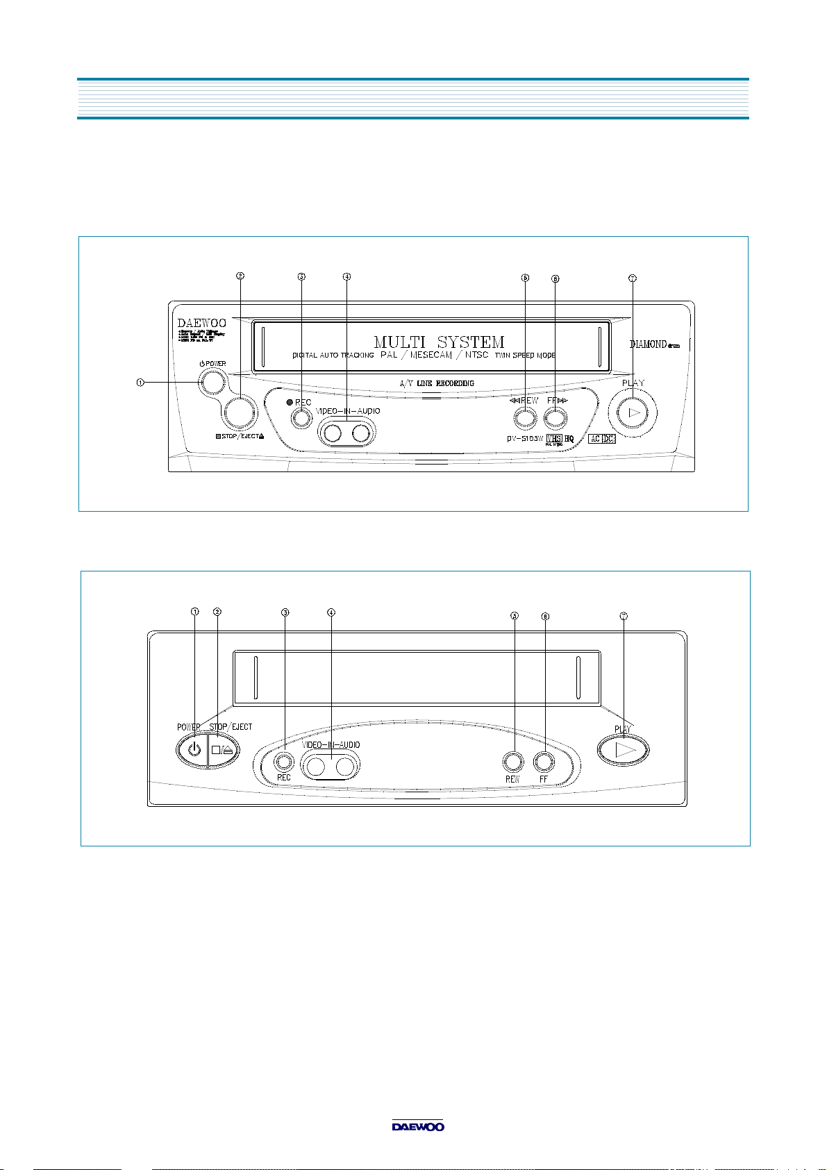
EXTERNAL VIEWS
1. FRONT VIEWS FUNCTION
DV-S103W FRONT VIEW
DV-S123W FRONT VIEW
POWER REVIND / REVIEW
STOP / EJECT FAST FORWARD / CUE
RECORD PLAY BACK
FRONT VIDEO AUDIO INPUT JACK
4
Page 6
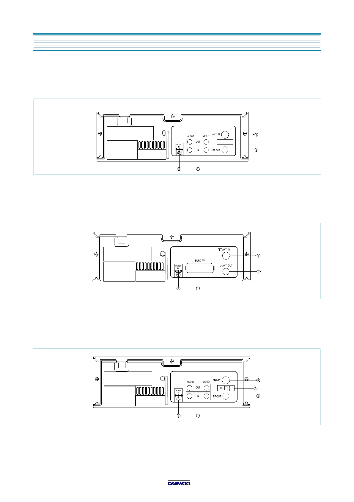
2. REAR VIEWS FUNCTION
DV-S103W & DV-S123W PHONE JACK TYPE REAR VIEW
AUDIO/ VIDEO IN/OUT JACK ANT INPUT
DC12V INPUT JACK RE OUTPUT
EXTERNAL VIEWS
DV-S103W & DV-S123W SCART JACK TYPE REAR VIEW
EURO AUDIO / VIDEO IN/OUT JACK ANT INPUT
DC12V INPUT JACK RF OUTPUT
DV-S103A & DV-S103N REAR VIEW
AUDIO / VIDEO IN/OUT JACK ANT INPUT
DC12V INPUT JACK RF OUTPUT
CH 3 OR 4 SELECT SWITCH
5
Page 7
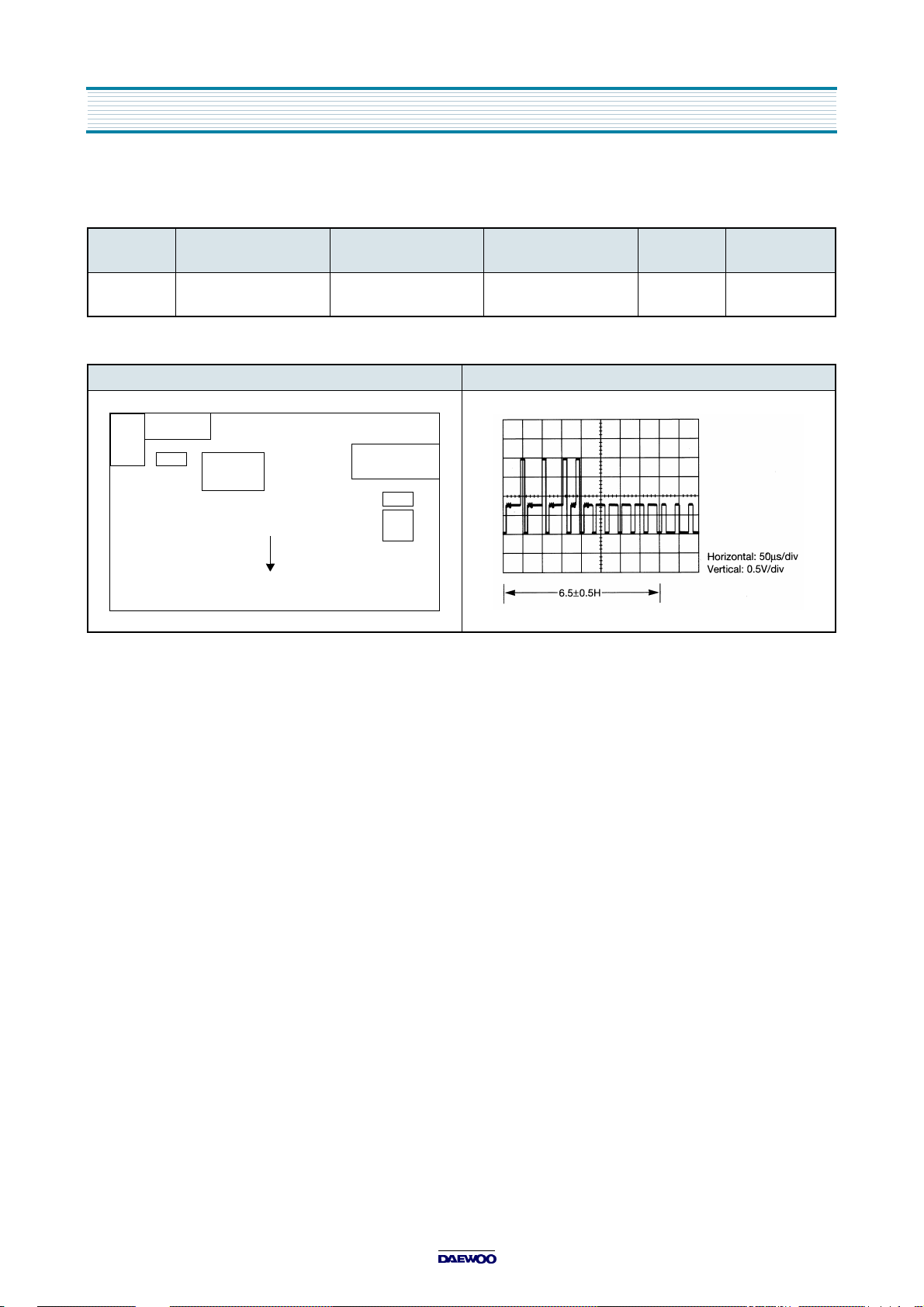
GENERAL ADJUSTMENT
SERVO CIRCUIT
ITEM
Playback
Phase
ADJUSTMENT
PARTS
R591
LOCATION OF ADJUSTMENT PARTS OBSERVATION WAVEFORM
A/V JACK
MOD
TJ391
(VIDEO OUT)
PRE-AMP
FRONT
ADJUSTMENT PROCEDURE
CHECK POINT TEST EQUIPMENTS MODE TEST TAPE
TJ591(V.SW)
TJ391(VIDEO OUT)
SMPS
TJ591
(V. SW)
R591
Oscilloscope Play DP-2
1. Preparation
Playback the test tape (DP-2).
Set the oscilloscope to the CHOP mode. Connect CH1 to the V.SW PULSE (TJ591) and CH2 to the VIDEO OUT
(TJ391) and trigger the scope with the signal from CH1.
2. Adjustment
Adjust R591 to the positive rising edge of V.SW PULSE at 6.5H ±0.5H from the V-SYNC.
3. Adjustment Inspection Standard
6.5H ± 0.5H
4. REMARKS
6
Page 8
SPECIFICATIONS
SYSTEM
Video signal
RF Output
VIDEO
Input : Video line in
Output : Video line out
Recording system
Signal to Noise ratio
Horizontal Resolution
AUDIO
Input : Audio line in
Output : Audio line out
Frequency Response
Signal to Noise Ratio
Audio Distortion
TAPE TRANSPORT
Format
Tape Width
Tape Speed
Maximum Recording Time
FF/REW time
GENERAL
Power Requirements
Power Consumption
Temperature
Operating position
DIMENSIONS
Carton size (W x H x D)
Set size (W x H x D)
Weight
PAL/MESECAM/NTSC color (for DV-S103W Series)
PAL-N/NTSC color (for DV-S103A Series)
NTSC color (for DV-S103N Series)
PAL-G/K/I UHF CH22 ~ CH40
(for DV-S103W & DV-S103S Series)
NTSC-M VHF CH3 OR CH4
(for DV-S103A & DV-S103N Series)
75 ohms unbalanced, sync.
75 ohms unbalanced, sync. Negative
Rotary tow-head helical scan
More than 45dB (PAL-SP)
More than 43dB (NTSC-SP)
240 Lines (PAL-SP)
210 Lines (NTSC-SP)
-8dBm, (CENELEC standard),
more than 47, unbalanced
-6dBm, (CENELEC standard),
less than 1, unbalanced
100Hz ~ 8KHz ( for PAL-SP)
100Hz ~10KHz (for NTSC-SP)
More than 38dB (for PAL-SP)
More than 40dB (for NTSC-SP)
Less than 3% (SP)
VHS standard
12.65 (1/2)
PAL SP : 23.39mm/sec
PAL LP :11.70mm/sec
NTSC-SP : 33.35/sec.
NTSC-EP : 11.12/sec.
480min, with E-240 tape (PAL-LP)
540min, with T-180 tape (NTSC-EP)
about 5min, with T-120 tape
AC 90V ~ 260V, 50/60Hz
DC12V ~ 16V (2A)
Max. 14W (in REC mode)
5°C ~ 35°C (Operating)
-20°C ~ 60°C (Storage)
Horizontal only
417 x 172 x 369 mm
280 x 91 x 347 mm
3.5 Kg
INPUT/OUTPUT JACK TYPE
Model For CIS For Middle East / Asia
Jack Type SCART Type
RCA Jack
(Phone Jack)
7
Page 9
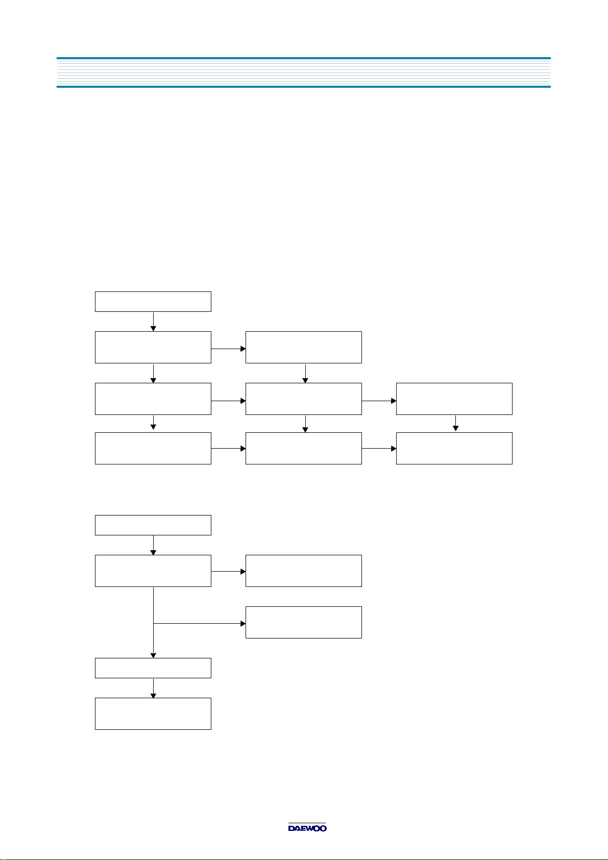
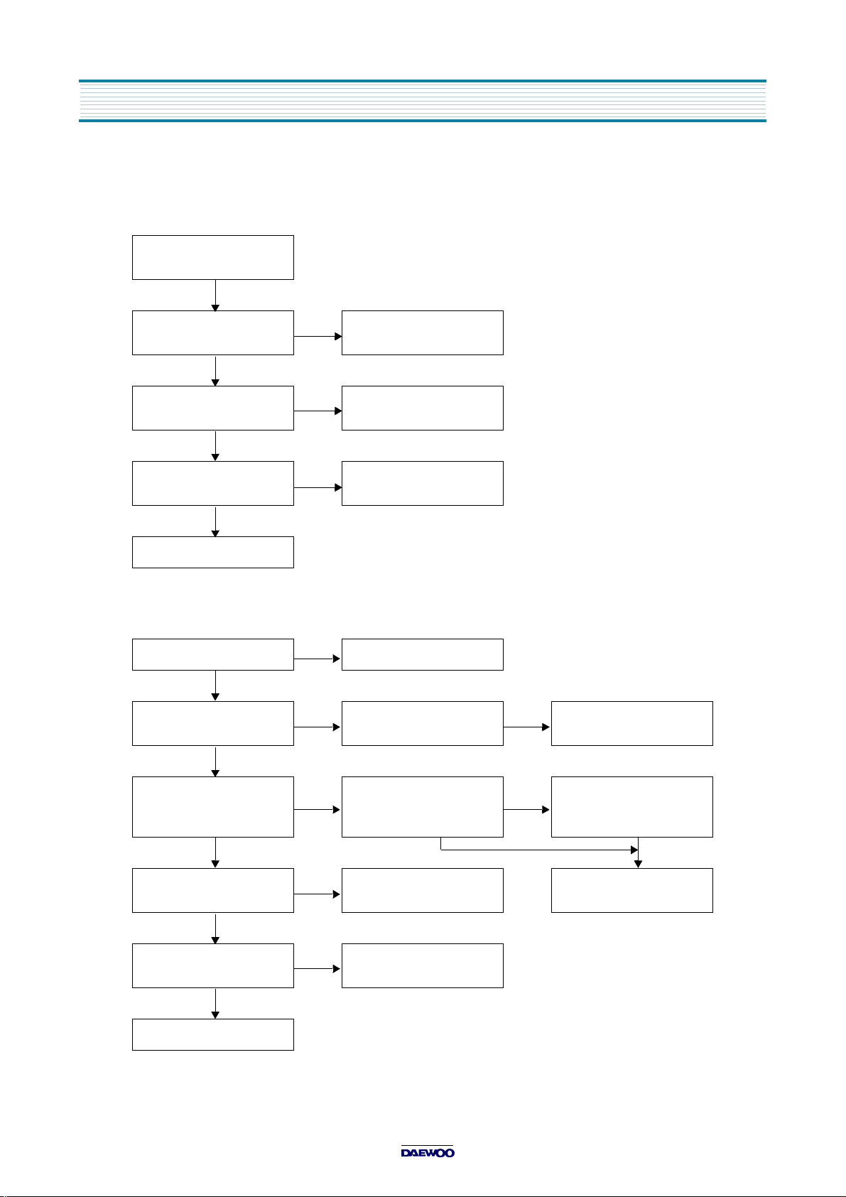
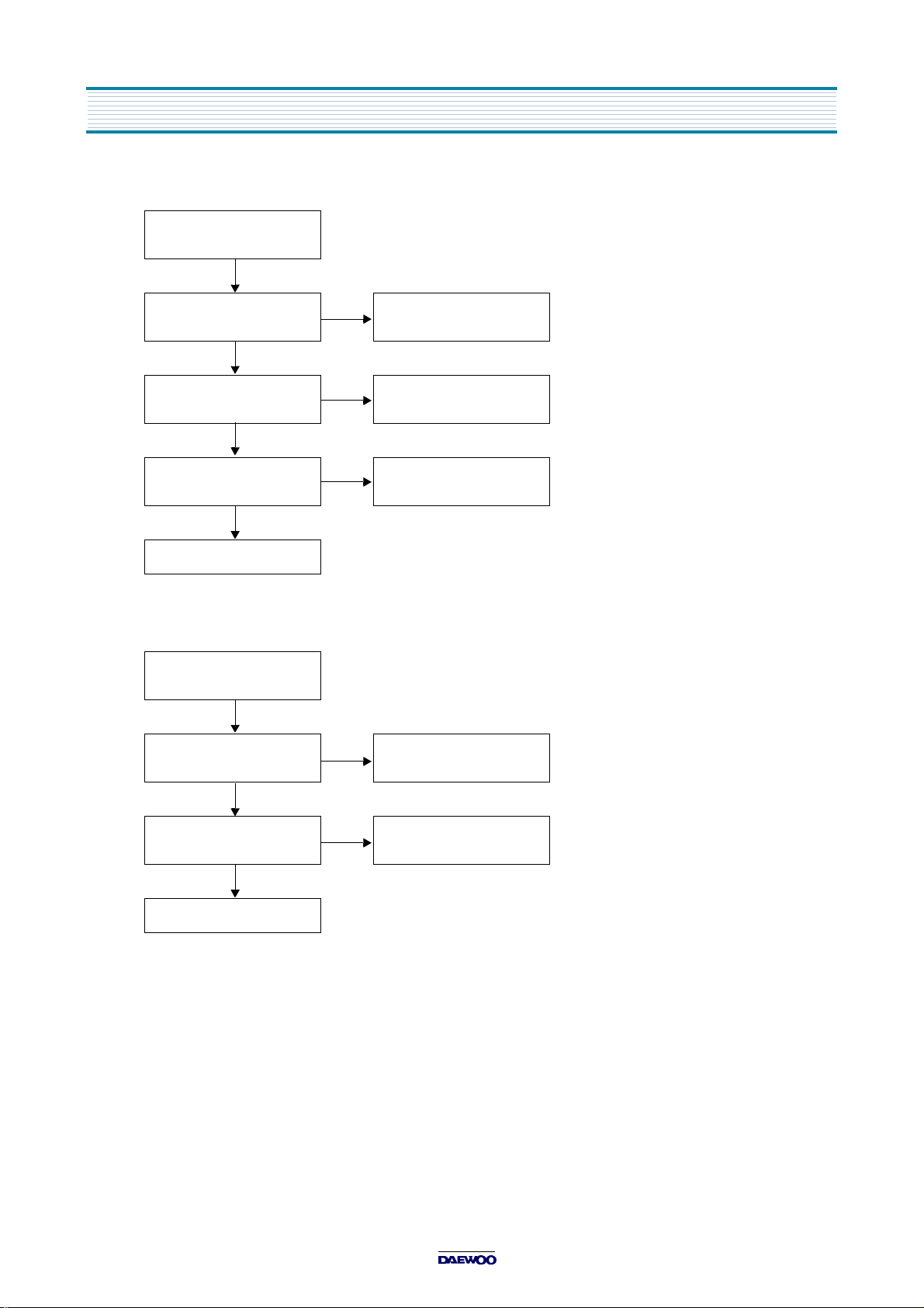
TROUBLE SHOOTING GUIDE
1. TROUBLE SHOOTING FLOW CHART
A. POWER CIRCUIT
When changing the parts which are out of order, first, remove the power plug from the socket and then discharge the
voltage across between both terminals of C803. (Use an external approximately 20 resistance)
When check the primary circuit by using the oscilloscopes insulate the oscilloscope properly (Use the insulating transformer)and GND must be connected GND into the primary GND (But there is no connection when checking the secaondary circuit.
When changing M801, check FUSE and ceramic resistor properly.
A-1. CHECKING THE PRIMARY CIRCUIT.
No output voltage
YES
Is the voltage applied to
CN11?
YES YES
Is the voltage +15V at pin3
of IC11?
YES YES YES
Check the secaondary
circuit
NO
NO
NO
Check F801, L801, L802
C803, D801, R801
Is the voltage above 10V
at pin3 of IC11?
( A )
NO
NO
A-2. CHECKING THE SECONDARDARY CIRCUIT.(Before secondary circuit open).
(A)
YES
Check each output voltage
YES
NO
NO
Check transformer of no
output stages
Check the diode of no
output stages
Is the voltage 0V at pin3
of IC11?
Check R14, R15, T11
R13, D11, L12
YES
Check the CN11
YES
Check the coil, condensor
of no output stages
8
Page 10
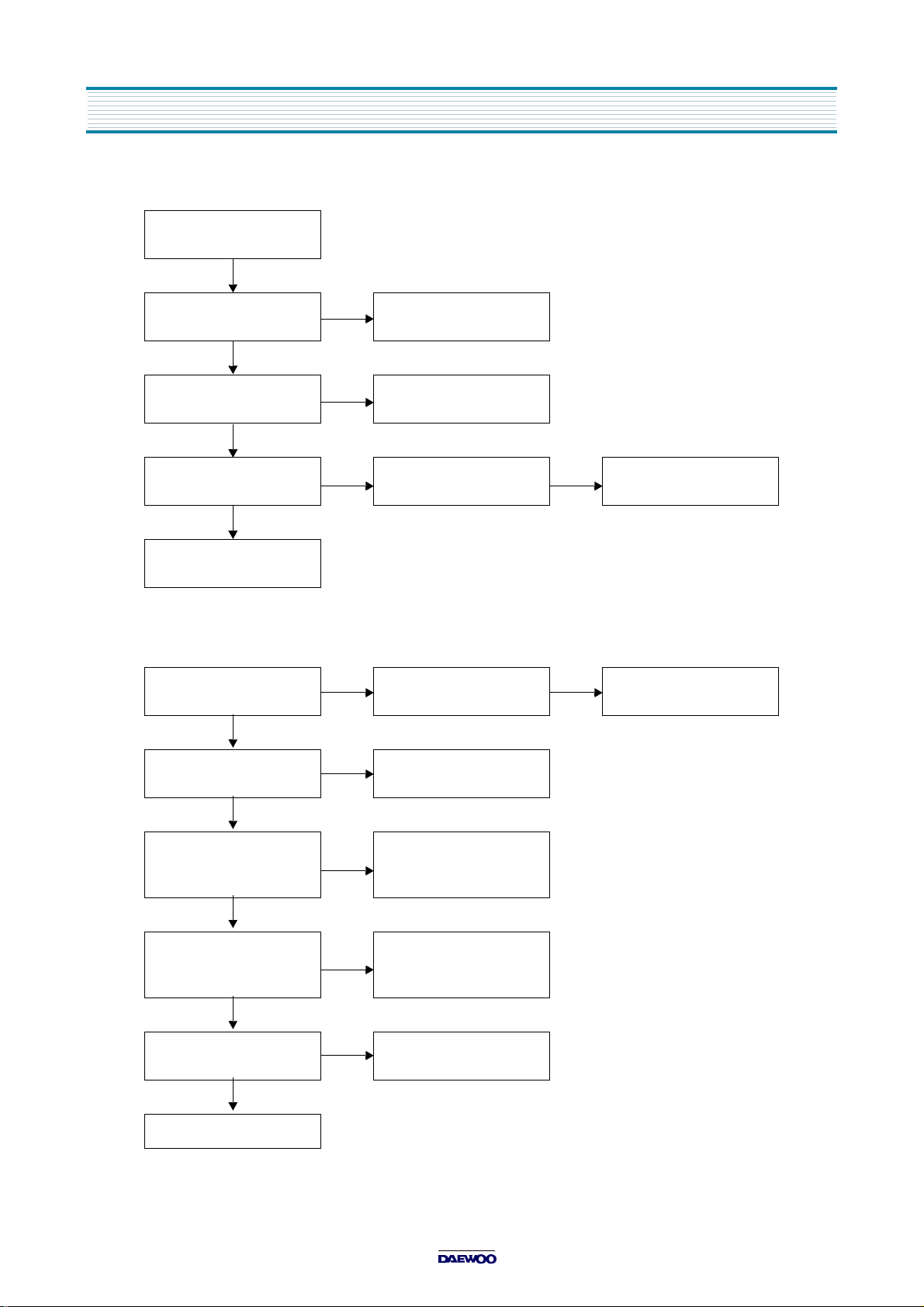
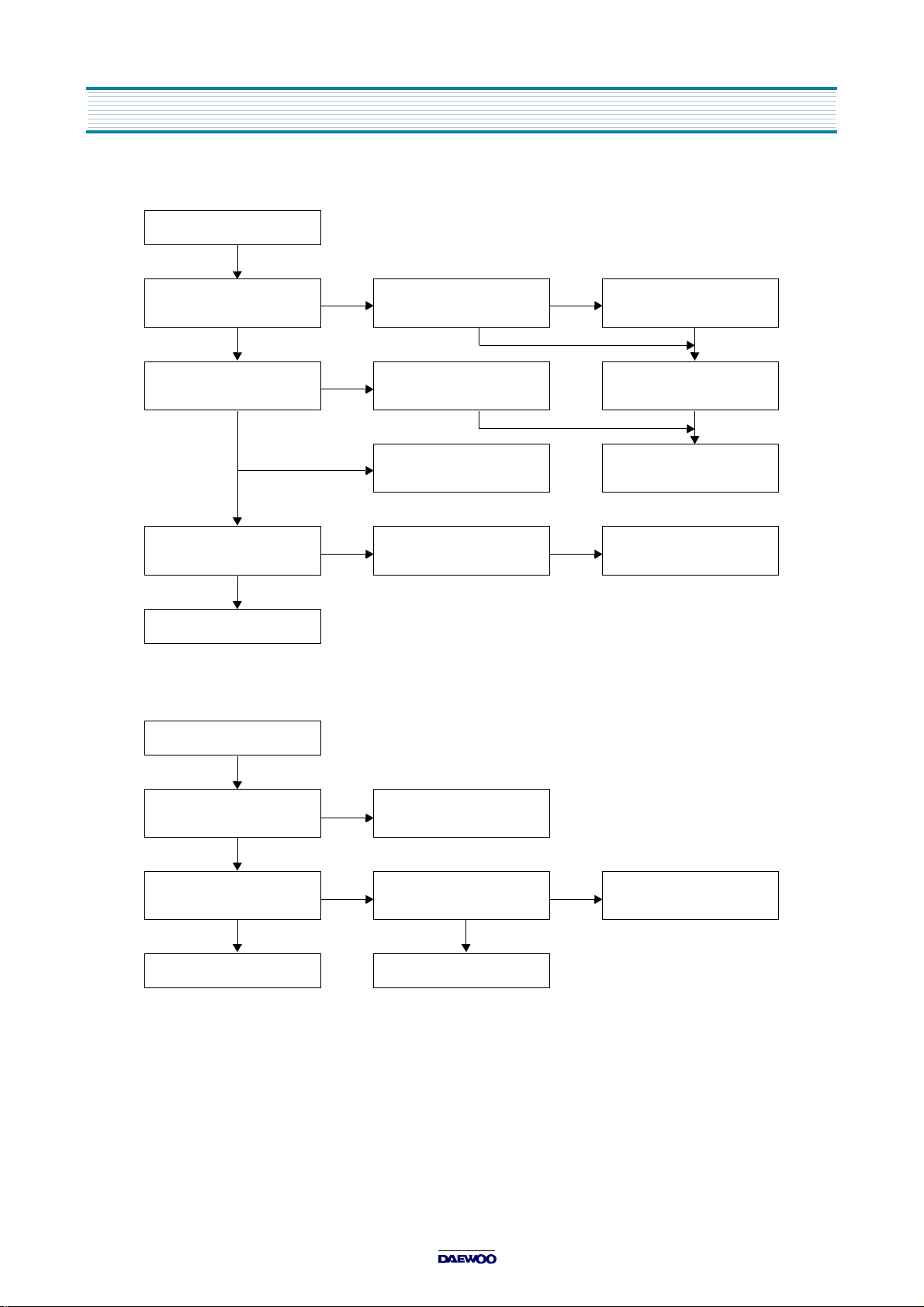
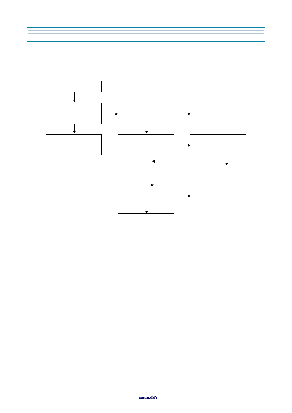
A-3. CHECKING THE DC - INPUT CIRCUIT.
Do not turn on the front
DISPLAY
YES
TROUBLE SHOOTING GUIDE
Check the polarity of
DC adaptor
YES
Is Vcc input at pin1 of
IC803?
YES
Check SERVO/SYSCON
circuit
YES
Check SERVO/SYSCON
circuit
B. LED DISPLAY CIRCUIT.
LED does not operate
properly.
YES
NO
NO
NO
NO
Change the DC adptor
Check JK801 and pattern
Is 1.25V input at pin4 of
Is +5.1V supplied from
D510 cathod to L701?
IC803?
NO
NO
Check R805, R806 and
R807
Check power module
Is +5.1V supplied to the
collectors of Q701~Q706?
YES
Are the signals supplied
from u-com to the bases
of Q701~Q706?
YES
Are the signals supplied
from u-com to the bases
of Q707~Q713?
YES
Are the signals supplied
To the LED(G701)?
YES
Check G701 and pattern
NO
NO
NO
NO
Check L701
Check u-com
Check u-com
Check Q701~ Q713 and
patterns
9
Page 11
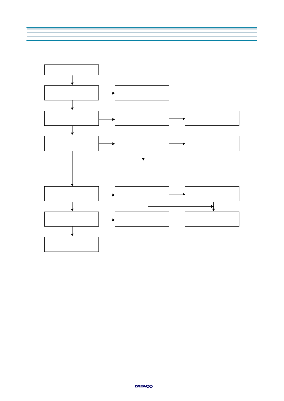
TROUBLE SHOOTING GUIDE
C. SERVO/SYSCON CIRCUIT
C-1. FRONT KEYS
Front keys do not operate
correctly
YES
Is +5.1V supplied to pin18
of IC501?
YES
Is +5.1V supplied to the
emitter of Q502?
YES
Is +5.1V input at pin41 of
IC501?
YES
Check IC501
C-2. PICTURE IN PB MODE
PB picture is not good
YES
Noise appears although
adjusting tracking?
NO
NO
NO
NO
NO
Check power module
Check u-com, JP053 and
JP059
Check Q502 and circuit
Adjust tracking
Noise appears although
Change cassette tape
YES
Check and re-adiust the
path of DECK
YES
Is CTL pulse output at
NO
pin1 of IC505?
YES YES
Is CTL pulse input at
NO
pin29 of IC501?
YES
The voltage of IC501's
NO
pin18 is not changing?
YES
Check IC501
AC HEAD's height is
normal and there is not
dust?
Check C556, C533 and
D505
Check power module
10
NO
Adjust the head height
and remove dust
Check IC505 and adjacent
YES
circuit
Page 12
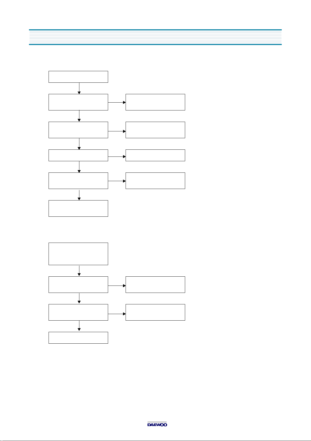
C-3. PICTURE IN PB MODE
PB picture is not good
YES
TROUBLE SHOOTING GUIDE
Noise appears on the
screen on the whole?
YES YES
Is V-SW puls applied to
PREAMP circuit?
YES
Is DC-ENVE waveform
input at pin39 of IC501?
YES
Check video circuit
C-4. AUTOSTOP IN PB MODE
Autostop during playback
NO
Noise appears on the
screen at the bottom?
NO
Is V-SW pulse supplied
From pin46 of IC501?
NO
NO
Check R524 and pattern
Is DC-ENVE waveform
output at pin6 of IC401?
YES
NO
Check flow C-2
Adjust the PG delay
Check D.PG input at pin13
of IC501 and P502
NO
Check video circuit
(R591)
YES
YES
Are S&T pulses input at
pin1 and pin7 of IC501?
YES
Is D.FG input at pin30 of
IC501?
YES
NO
NO
Check reel sensors
Is D.PWM output at pin33
of IC501?
YES
Check IC501 Check P502 and R536
NO
Check IC501
11
Page 13
TROUBLE SHOOTING GUIDE
C-5. CASSETTE IS NOT INSERTED
Cassette is not inserted
YES
Is ON/OFF 12V supplied
NO
at pin7 of IC503?
YES
CAM data are changed
NO
when CST IN?
YES
Is +5V applied to pin6
NO
of IC503 when CST IN?
YES YES
Is 8.2V supplied to pin4
of IC503?
YES
Are control signals output
NO
at pin76 and 78 of IC501?
NO
at pin2 and 10 of IC503
Check power module
Check P504
Is control signal output
at pin76 of IC501?
Check pattern and R529
Are control signals output
YES
Check IC503
NO
NO
NO
Check DECK
Check IC501
Check IC503
YES
Check D504, D508 and
D503
YES
Check P503 and L/C
Motor.
12
Page 14
C-6. CAPSTAN MOTOR
Capstan M/T loading stops
YES
TROUBLE SHOOTING GUIDE
Is +14V supplied to pin7
NO
of P501?
YES
Is the input of P502's pin6
NO
2.5 ~ 3.5V?
YES
Is pin4 of P501 2.5V?
YES
Is C.PWM output at pin34
NO
NO
of IC501?
YES
Check P501, R516, R526
and C526
C-7. DRUM & CAPSTAN M/T IN REC MODE
Drum M/T and capstan
M/T rotate at reular speed
(IN REC MODE)
Check power module
Check circuit of R555,
R556 and R557
Check R559 and R560
Check IC501
YES
Is C.SYNC applied to the
base of Q501?
YES
Is V.SYNC input at pin28
of IC501?
YES
Check motors
NO
NO
Check C.SYNC of IC301
and pattern
Check Q501 and R527
13
Page 15
TROUBLE SHOOTING GUIDE
C-8. EMERGENCY
Emergency mode when
plugging (power cord)
YES
Is +5.1V applied to pin18
of IC501?
YES
Does X501 crysyal
oscillate?
YES
Are CAM SW data cor-
rect?
YES
NO
NO
NO
Check power module
Check IC501 and crystal
circuit
Recheck P504 and CAM
SW contact
Check IC503 and IC501
C-9. VCP DOES NOT OPERATE (ALTHOUGH POWER CIRCUIT IS NORMAL.)
VCP does not operate after
power cord plugging
YES
Is +5.1V supplied to pin1
of IC502?
NO
Check power module
YES
Is +5V input at pin63 of
IC501?
YES
Check flow C-8
NO
Check IC502 and pattern
14
Page 16
D. AUDIO CIRCUIT
D-1. PB MODE
No sound in the PB mode
YES
TROUBLE SHOOTING GUIDE
NO
Is the output at pin77 of
Is +5V supplied to pin76 of
IC301?
YES YES
Check R217, R218, L602
Is voltage less than 0.2V
and pattern
Is collector of Q204 GND?
IC301 and to pin2 of
T201?
at pin80 of IC301?
YES
YES
Check pattern and AC
Head
NO
Check IC802 and adjacent
NO
Are CLK and DATA
applied to pin63 and 64 of
YES NO
Check IC501
NO
Check Q202, Q203 and
circuit
IC301?
Q204
15
Page 17

TROUBLE SHOOTING GUIDE
D-2. NO SOUND IN THE PB MODE AFTER RECORDING
IN REC MODE
Is signal audio input into
pin71 of IC301?
YES
Is +5V applied to pin76
and 47 of IC301?
YES
Is the voltage above 4V at
pin80 of IC301?
YES
Is audio signal input into
pin79 of IC301?
YES
Does pin6 of T201
Oscillate?
YES
AC signal put on 70KHz
at base of Q201?
NO
NO
NO
Check R609, R610 and
Check IC802 and adjacent
Is CLK and DATA applied
to pin63 and 64 of
NO
Check C212, R215, R214
and C210
NO
Is the volatge from 0.7V
to 3.0V at pin5 of IC301?
YES
JK603
circuit
IC301?
YES
NO
NO
Check IC501
YES
AC signal is put on the
DC voltage at pin5 of
IC301?
YES
Check AC head
YES
Clean head
Check T201's circuit
Is the voltage from 0.7V
to 0.8V at pin6 of IC301?
YES
Check Q205
16
NO
Check IC301
Page 18

TROUBLE SHOOTING GUIDE
D-3. EE MODE
No sound in the EE mode
Is signal input into pin71
Is signal output at pin77 of
Check C212, R217, R218
YES
Is video signal input at
pin30 of IC301?
YES
of IC301?
YES
IC301?
YES
C213 and L602
NO
NO
TO VIDEO EE MODE
Check R609, R610, C218
and JK603
NO
Is +5V applied to pin76
and 47 of IC301?
YES
Are CLK and DATA input
at pin63 and 64 of IC301?
YES
Check IC301
NO
NO
Check IC802 and
adjacent circuit
Check SERVO/SYSCON
17
Page 19

TROUBLE SHOOTING GUIDE
E. VIDEO CIRCUIT
E-1. EE MODE
No output at pin19 of
JK601 or JK602?
YES
Is ON/OFF 12V supplied
to R603 and R604?
YES
Is video signal output at
pin38 of IC301?
YES
Check R312, Q604 and
Adjacent circuit
NO
Check IC801 and adjacent
NO
Is video signal input at
pin30 of IC301?
Are CLK & DATA signals
input at pin63 and 64 of
Is ON/OFF 5V supplied at
pin47 and 76 of IC301?
Do X301 and X302
Check IC301
circuit
YES
IC301?
YES
YES
oscillate?
YES
NO
NO
Check JK603 and pattern
Check SERVO/SYSCON
circuit and pattern
NO
Check IC802 and adjacent
NO
Check X301 and X302
circuit
18
Page 20

E-2. PREAMP IN THE PAYBACKMODE
TROUBLE SHOOTING GUIDE
Is signal from heads fed to
pin1 and 3 of P401?
YES
Is ON/OFF5V from pin76
of IC301 supplied to
pin131 of IC401 at 5V?
YES
Is REC(H) from pin79 of
IC501 supplied to pin11
of IC401 at 0V?
YES
Is V.SW pulse from pin46
of IC501 supplied to
pin4 of IC401?
YES
Is the signal from pin1 and
3 of P401 fed to pin17
or 19 of IC401?
NO
NO
NO
NO
NO
Check the DRUM and
DECK mechanism
Check the ON/OFF 5V
Check Q503, Q504 and
adjacent circuit
Check SERVO/SYSCON
Change IC401
YES
Is the signal from pin7 of
NO
IC401 fed to C416?
YES
TO LUMINANCE
SIGNAL IN THE REC
MODE
NOTE : 1) REC(H) : "HIGH" in the REC mode.
"LOW" in the EE and PB mode
Check Q401 and adjacent
circuit
19
Page 21

TROUBLE SHOOTING GUIDE
E-3. LUMINANCE IN THE PALYBACK MODE
Is the RF signal obtained
from pin13 of IC401?
YES
Is the RF signal from pin7
of IC301?
YES
Is ON/OFF 5V supplied to
pin36 and 47 of IC301?
YES
Is the luminance signal
from pin15 fed to pin20
of IC301 through Q302?
YES
Is the luminance signal
from 26 fed to pin38 of
IC301?
YES
To output buffer circuit
( Check Q604 and
adjacent circuit )
NO
TO PREAMP IN THE
PLAYBACK MODE
NO
Check Q401 and adjacent
NO
NO
NO
Check the ON/OFF 5V
Check Q302 and adjacent
Circuit
Check IC301
20
Page 22

E-4. COLOUR IN THE PLAYBACK MODE
TROUBLE SHOOTING GUIDE
Is the RF signal obtained
from pin13 of IC401?
YES
Is the RF signal from pin13
of IC401 fed to pin15 of
IC301?
YES
Is ON/OFF 5V supplied to
pin36 and 47 of IC301?
YES
Is the colour signal from
pin15 of IC301 fed to
pin48 and 50 of IC301?
YES
Is the colour sinal from
pin48 and 50 of IC301
fed to pin13 of IC302?
YES
NO
TO PREAMP IN THE
PLAYBACK MODE
NO
Check Q401, adjacent
and PCB pattern
NO
NO
Check the ON/OFF 5V
Check IC301
NO
Check C351, C354, IC302
and adjacent circuit
Is the colour signal from
pin13 of IC302 fed to
pin45 of IC301 through
pin52 and 46?
YES
Is the C.ROTARY supplied
to pin66 of IC301?
YES
To output buffer circuit
NO
NO
Check Q304, C332, and
R317
Check C.ROTARY
21
Page 23

TROUBLE SHOOTING GUIDE
E-5. PREAMP CIRCUIT IN THE RECORD MODE
Is the Y.FM signal from
pin18 of IC301 fed to
pin9 of IC401?
YES YES
Is the down converted
Colour signal from pin14
of IC301 fed to pin10 of
IC401?
YES YES
Is ON/OFF 5V supplied to
pin13 of IC401 at 5V?
YES
NO
NO
NO
Check R305, C405
correct?
TO LUMINANCE
SIGNAL IN THE REC
MODE
Check C406 correct?
TO COLOUR SIGNAL
IN THE REC MODE
Check ON/OFF 5V
NO
NO
Change damaged
components
Changed damaged
Components
Is REC(H) supplied to
pin11 of IC401 at 5V?
YES
Is the signal from pin9 and
10 fed to pin17 of IC401?
YES
Change DRUM
NO
Check REC(H) or Q503,
Q504 and adjacent circuit
NO
NO
Changed IC401
Check Q401 and PCB
pattern
22
Page 24

E-6. LUMINANCE SIGNAL IN THE RECORD MODE
TROUBLE SHOOTING GUIDE
Is ON/OFFF 5V supplied
to pin36 and 47 of IC301?
YES
Is the obtained from pin34
of IC301?
YES
Is the signal from pin34 of
IC301 fed to pin25 of
IC301?
YES
Is the luminance signal
from pin25 fed to pin26 of
IC301?
YES YES
NO
NO
NO
Check the ON/OFF 5V
TO EE MODE
Is C319 correct?
Check IC301
NO
Are Q302, C312, C313,
C342, R307, R308, R309
and R310 correct?
Check IC301
YES
NO
NO
Change damaged
Compoents
Changed damaged
Components
Is the luminance signal
from pin26 fed to pin18
of IC301?
YES
Is the modulated lumi-
nance
signal from pin18 of IC301
fed to pin9 of IC401?
YES
To preamp circuit in the rec
mode
NO
Check IC301
NO
Check R305 and C405
23
Page 25

TROUBLE SHOOTING GUIDE
E-7. COLOUR SIGNAL IN THE RECORD MODE
Is ON/OFF 5V supplied to
pin36 and 47 of IC301?
YES
Is the obtained from pin34
of IC301?
YES
Is the colour signal from
pin50 of IC301 to pin52
of IC301?
YES
Is the down converted
colour signal from pin14
of IC301 fed to pin10 of
IC401 through C406?
YES YES
TO PREAMP CIRCUIT
IN THE REC MODE
F. MODULATOR CIRCUIT
NO
NO
NO
NO
NO
Check the ON/OFF 5V
TO EE MODE
Check IC302, PCB .and
adjacent circuit
Check IC302, PCB and
adjacent circuit
Check IC301
NO
Changed damaged
components
F-1. NO MODULATOR OUTPUT
Check the output channel
of VCP and input
channel of TV?
YES
Are +5V & ON/OFF 5V
applied to pin1 and 4 of
RF101?
YES
Is ON/OFF 12V applied to
pin7 of RF101?
YES
Are video and audio signal
input into pin2 and 6 of
RF101?
YES
Are CLK & DATA signal
input into pin3 and 5 of
RF101?
YES
NO
Set the output channel of
VCP reference to owners
Mannual
NO
Check ON/OFF 5V and
the option circuit
according to the option table
NO
NO
Check RJ013 and IC801
Check A/V circuit
NO
Check SERVO/SYSCON
circuit
Check RF101
24
Page 26

2. VOLTAGE CHART
IC301 : A/V IC ( LA71501M )
TROUBLE SHOOTING GUIDE
MODE
PIN.NO.
1 2.44 2.40 21 0.35 0.39 41 0.06 61 2.05 2.02
2 0.01 0.00 22 1.56 2.25 42 2.00 62 0.21 0.26
3 2.44 2.41 23 0.02 1.80 43 0.48 63 4.48 4.48
4 1.03 0.05 24 2.41 1.82 44 1.83 64 4.75 4.75
5 1.35 5.51 25 2.15 2.08 45 1.96 65 0.31 0.31
6 0.86 0.02 26 3.08 3.03 46 0.03 66 0.00 0.40
7 2.42 2.39 27 0.00 0.06 47 5.09 67 0.04 0.04
8 2.46 2.40 28 1.08 0.28 48 2.85 68 0.06 0.61
9 2.37 2.37 29 1.90 2.16 49 4.42 69 5.09 5.08
10 2.37 2.37 30 2.11 0.00 50 2.92 70 0.02 0.00
11 3.07 2.38 31 4.08 4.08 51 4.23 71 2.39 2.38
12 2.32 2.31 32 1.80 0.28 52 3.22 72 0.01 0.01
13 1.71 2.08 33 0.58 0.58 53 0.00 73 2.39 2.38
14 2.95 0.31 34 2.17 0.00 54 2.15 74 2.41 2.40
15 0.00 3.25 35 3.14 3.16 55 5.15 75 2.39 2.38
16 2.56 2.59 36 5.09 5.06 56 5.15 76 5.15 5.14
17 3.32 1.64 37 0.59 0.59 57 0.01 77 2.49 2.48
18 2.11 2.56 38 1.70 1.78 58 0.19 78 0.00 0.00
19 4.30 0.08 39 3.19 3.18 59 2.46 79 2.40 2.38
20 3.14 3.05 40 3.01 3.00 60 4.07 80 5.14 0.15
REC PB
MODE
PIN.NO.
REC PB
MODE
PIN.NO.
REC PB
MODE
PIN.NO.
REC PB
POWER IC
MODE
PIN.NO.
1 15.0 6.0 Vcc
2 12.5 5.2 6.6
3 GND GND GND
4 6.0 6.0 1.25
IC801 IC802 IC803
IC504 : OP-AMP IC ( KA4558 / MC4558 )
MODE
PIN.NO.
1 3.04 3.50 5 3.04 3.40
2 3.04 3.40 6 3.04 3.40
3 3.04 3.40 7 3.04 3.40
4 8 5.90 5.90
REC PB
MODE
PIN.NO.
REC PB
25
Page 27

TROUBLE SHOOTING GUIDE
3. WAVEFORMS ON VIDEO CIRCUIT
WAVEFORMS IN THE EE MODE(COLOR BAR INPUT)
1 Pin 30 of IC301
(SECAM color bar input :
1.0Vp-p
2 Pin 30 of IC301
(PAL color bar input :
1.0Vp-p)
3 Pin 38 of IC301
(PAL color bar output :
2.0Vp-p)
WAVEFORMS OF THE LUMINANCE IN THE RECORD MODE(COLOR BAR INPUT)
4 Pin 18 of IC301(PAL)
(REC luminance :
300mVp-p)
6 Pin 25 of IC301
(0.5Vp-p)
7 Pin 26 of IC301
(0.5Vp-p)
8 Pin 35 of IC301
(Color bar input :
1.0Vp-p)
9 Pin 40 of IC301
(0.4Vp-p)
10
Pin 42 of IC301
(0.4Vp-p)
11 Pin 10 of IC302
(fsc=3.579545MHz :
350mVp-p)
26
Page 28

TROUBLE SHOOTING GUIDE
WAVEFORM OF THE PAL COLOR IN THE RECORD MODE(COLOR BAR INPUT)
12
Pin 35 of IC301
(PAL color input :
1.0Vp-p)
Pin 48 and 50 of IC301
13 14
(300mVp-p)
Pin 52 of IC301
(400mVp-p)
Pin 37 of IC301
(C.SYNC : 2Vp-p)
Pin 14 of IC301
1615
(300mVp-p)
WAVEFORMS OF THE LUMINANCE IN THE PB MODE (DP-1 TEST TAPE)
23
UP : Pin 66 of IC301(color
rotary : 1Vp-p
DOWN : Pin 20 of IC301
(ENVE : 0.5Vp-p)
Pin 25 of IC301
24 25
(0.5Vp-p)
17
Pin 10 of IC401
(REC PAL color :
300mVp-p)
Pin 26 of IC301
(0.5Vp-p)
26
Pin 38 of IC301
(Video out : 2.0Vp-p)
Pin 40 of IC301
27
(400mVp-p)
27
Pin 42 of IC301
28
(300mVp-p)
Page 29

TROUBLE SHOOTING GUIDE
WAVEFORMS OF THE LUMINANCE IN THE PB MODE (DP-1 TEST TAPE)
UP : Pin 66 of IC301(color)
29
rotary : 0.5Vp-p)
DOWN : Pin 20 of IC301
(500mVp-p)
Pin 52 of IC301
(300mVp-p)
Pin 37 of IC301
30
(Video out : 2.0Vp-p)
Pin 45 of IC301
(500mVp-p)
Pin 48 and 50 of IC301
31
(240mVp-p)
Pin 46 of IC301
343332
(500mVp-p)
28
Page 30

TROUBLE SHOOTING GUIDE
4. ¥ì-COM PIN ASSIGNMENT
P : Pulse H : High L : Low
No. NAME I/O ASSIGNMENT ACTIVE CN
1 N.C
2 T_ REEL I TAKE-UP REEL PULSE P DECK(REEL)
3 A_MUTE(H) O AUDIO MUTE H OUTPUT H A/V
4 SLOW CTL O N.C
5 MESECAM(H) I MESECAM MODE INPUT H A/V
6 S_REEL I SUPPLY REEL PULSE P DECK(REEL)
7 SECAM_EE(H) O SECAM EE MODE OUTPUT H SECAM_L
8 S_DATA O A/V SERIAL DATA OUTPUT P A/V
9 S_CLK O A/V SERIAL CLK OUTPUT P A/V
TV/VCR MODE SWITCHING
10 TV(L)/VCR(H) O
11 MOD_CLK O MODULATOR CLK OUTPUT P RF101, IC505
12 MOD_DATA O MODULATOR DATA OUTPUT P RF101, IC505
13 D_PG I DRUM PG INPUT P DECK(DRUM)
14 PWR ON(L) O POWER ON/OFF CONTROL L POWER
15 REMOTE I REMOTE DATA INPUT P R_RECEIVER
16 CAP_I-LIMIT O
17 N.C
18 Vdd2 Vcc = +5V
19 GRID_1 O LED GRID_1 OUTPUT P LDISPLAY
20 GRID_2 O LED GRID_2 OUTPUT P L-DISPLAY
21 GRID_3 O LED GRID_3 OUTPUT P L-DISPLAY
22 GRID_4 O LED GRID_4 OUTPUT P L-DISPLAY
23 N.C GND
24 N.C GND
25 N.C GND
26 N.C GND
27 REC_CTL O CTL PULSE OUT IN REC MODE P DECK(CTL)
28 V_SYNC I V_SYNC DATA INPUT P A/V
29 PB_CTL I CTL INPUT IN PB MODE P DECK(CTL)
30 D_FG I DRUM FG INPUT P DECK(DRUM)
31 C_FG I CAPSTAN FG INPUT P DECK(CAPSTAN)
32 Vss2 GND
33 D_PWM O DRUM M/T CONTROL PWM P DECK(DRUM)
ON TV
TV : L VCR : H
THIS PORT IS USUALLY OPEN BUT
OUPUTS FOR FRAME ADVANCE
H/L
L/P
SYSTEM
OPTION
DECK
(CAPSTAN)
29
Page 31

TROUBLE SHOOTING GUIDE
No. NAME I/O ASSIGNMENT ACTIVE CN
34 C_PWM O CAPSTAN M/T CONTROL PWM P DECK(CAPSTAN)
35 SYSSEL1 I DONT CARE
36 SYSSEL2 I
37 N.C GND
38 DC_ENVE I DC_ENVE INPUT IN PB MODE PREAMP
39 TRKDLY I
40 AVss GND
41 PG_DLY I PG DELAY INPUT TO ADJUST 6.5H DC DECK & R591
42 KEY1 I FRONT PANNEL KEYS DATA INPUT DC A/V IN/OUT
43 AD_DET I TO DETECT +5V EVEL DC +5V
44 AVref I Vcc FOR u-COMS AD BLOCK
45 C_SYNC I C_SYNC INPUT P A/V
46 V_SW O VIDEO SWITCHING PULSE OUTPUT P PREAMP
47 QV_SYNC O OUPUT DURING TRICK MODE P/L A/V
48 C_ROT O INVERTED V_SW PULSE P A/V
49 GRID_5 O LED GRID_5 OUTPUT P L-DISPLAY
SYSTEM SELECT INPUT
( Reference to SERVO/SYSCON circuit)
TRACKING DELAY IN
MANUAL TRACKING
DC
DC PATH JIG
50 CAM_C
51 CAM_B
52
53 REC_SAFETY(L) I
54 N.C GND
55 T_END(H) I TAPE END SENSOR INPUT H DECK
56 SECAM(H) I SECAM MODE INPUT H SECAM-L
57 T_START(H) I TAPE START SENSOR INPUT H DECK
58 OSC_IN I 8MHz OSC INPUT
59 OSC_OUT O 8MHz OSC OUTPUT
60 Vss1 CRYSTAL GND
61 N.C OPEN
62 N.C OPEN
CAM_A
I DECK (CAM SW)
CAM_A CAM_B CAM_C MODE
H H H CAM OFF
L H L EJECT
H H L STAND-BY
H L H FF/REW
L L L BRAKE
L L H REV
L H H STOP/PLAY/CUE
REC SAFETY TAB IS DETECTED L
STATE SO THAT RECORDING IS
INHIBITED
L REC SAFETY SW
30
Page 32

TROUBLE SHOOTING GUIDE
No. NAME I/O ASSIGNMENT ACTIVE CN
63 RESET(L) RESET INPUT L
64 N.C GND
65 N.C GND
66 SEG_7 O LED SEGMENT_7 OUTPUT P L-DISPLAY
67 SEG_6 O LED SEGMENT_6 OUTPUT P L-DISPLAY
68 SEG_1 O LED SEGMENT_1 OUTPUT P L-DISPLAY
69 SEG_2 O LED SEGMENT_2 OUTPUT P L-DISPLAY
70 SEG_3 O LED SEGMENT_3 OUTPUT P L-DISPLAY
71 SEG_4 O LED SEGMENT_4 OUTPUT P L-DISPLAY
72 SEG_5 O LED SEGMENT_5 OUTPUT P L-DISPLAY
73 Vdd1 Vcc
74 A/D RESET(H) O TO RESET AVref H
75 CAP_F/R O CAP-M/T FORWARD(L)/REVERSE(H) L/H DECK CAP.
76 LM_R
77 LM_F
78 CST IN(L) O
79 REC(H) O TO OUTPUT DURING RECORDING H A/V, PREAMP
80 GRID_6 O LED GRID_6 OUTPUT P L-DISPLAY
O
O
LM_R LM_F STATE
L H OFF
L H REVERSE
H L FORWARD
H H BRAKE
TO OUTPUT L STATE IN CASSETTE
IN MODE ( PLAY, FF/REW, CUE/REV,
SLOW, STILL AND STOP ETC. )
H/L
DECK LM M/T
(IC503)
L
DECK LM M/T
( IC503 )
31
Page 33

PRINTED CIRCUIT BOARD
1. PCB MAIN
32
Page 34

2. PCB POWER(SMPS)
PRINTED CIRCUIT BOARD
33
Page 35

CIRCUIT DIAGRAM
1. CONNECTION DIAGRAM (DV-S103W/S103A/S103N)
34
Page 36

2. POWER CIRCUIT (DV-S103W)
CIRCUIT DIAGRAM
35
Page 37

CIRCUIT DIAGRAM
3. SERVO SYSCON CIRCUIT (DV-S103W)
36
Page 38

4. AV INPUT OUTPUT CIRCUIT (DV-S103W)
CIRCUIT DIAGRAM
37
Page 39

CIRCUIT DIAGRAM
5. VIDEO AUDIO CIRCUIT (DV-S103W/S103A/S103N/S103S)
38
Page 40

EXPLODING VIEWS & PARTS LIST
1. PACKING AS
39
Page 41

EXPLODING VIEWS & PARTS LIST
2. SET TOTAL ASSEMBLY
40
Page 42

3. FRONT PANEL ASSEMBLY
DV-S103W FRONT PANEL ASSEMBLY
EXPLODING VIEWS & PARTS LIST
41
Page 43

EXPLODING VIEWS & PARTS LIST
DV-S123W FRONT PANEL ASSEMBLY
42
Page 44

ELECTRICAL PARTS LIST
1. PCB MAIN AS
LOC PART-CODE PART-NAME PART-DESC
1 PVACPSD360 ACCESSORY AS F342DY(BT:AAM)
D001 97P9560000 MANUAL OWNERS ALL MODEL
D002 97P881RP10 CABLE RF PAL 1.0M
D003 97P0424100 COVER ACCESSORY LD-PE T0.1
D004 47P7500002 BATTERY AAM 1.5V(SUPERGARD)
3 PVMCASW068 CHASSIS MAIN AS S123W-QB(W066-C)
A001 97P0610200 CHASSIS MAIN HI-PS(HB)
A015 97P0473800 COVER PRE AMP ET T0.3
A0151 7003300611 SCREW MACHINE BIN 3X6 MFZN
A040 97P0469100 COVER TOP SECC T0.5+PCM
A041 7173401212 SCREW TAPPTITE TT2 BIN 4X12 BK
A060 97P0476100 COVER BOTTOM SECC T0.5
A061 7173401211 SCREW TAPPTITE TT2 BIN 4X12 MFZN
D100 97P1R2B300 REMOCON HANDSET AS VR-F2B3
F801 5FSCB2022S FUSE CERA SEMKO T2AH 250V MF51
M01 97PP321200 PANEL FRONT AS S123
M021 7173401211 SCREW TAPPTITE TT2 BIN 4X12 MFZN
M1000 97PC0237D- DECK TOTAL AS S2-M(PAL 2HD LP NON)
PW01 97P69DB900 CORD POWER AS EUROPEAN
0M801 PVPWSWW063 AUTO VOLT REGULATOR S103WY-QB/D(F13-S,M-IN)
CN11 97P6284000 CONN WAFER YFAW025-105 ANGLE 3.5X4.5
CN21 97P6284000 CONN WAFER YFAW025-105 ANGLE 3.5X4.5
C19 CCXB3A102K C CERA 1KV B 1000PF K (TAPPING)
C20 CBXB3A470J C CERA SEMI 1KV SL 47PF J HR
C21 CEXF1A102F C ELECTRO 10V RX 1000MF 10X20
C23 CEXF1E471F C ELECTRO 25V RX 470MF 10X20
DZ11 DZP6KE250A DIODE ZENER P6KE250A
D21 D31DQ09--F DIODE SCHOTTKY 31DQ09-FC5
D21A 56X0000008 COIL BEAD OP5*5*2.5H
D22 DS2L20U--F DIODE S2L20U 4004 P15
D22A 56X0000008 COIL BEAD OP5*5*2.5H
IC11 1KA1L0380R IC POWER SW KA1L0380RB-YDTU
L12 56X0000007 COIL BEAD BI-4865(5TS) BASE
M801A 97PC316600 COVER SHI SMPS AS DV-S103
M801B 97P0970501 PLATE SHI SMPS ET T=0.5
M801C 97P5603700 INSULATION SMPS PC T0.5
PC11 1PC123FY8- IC PHOTO COUPLER PC123FY8 CTR100-200
R13 RS02F334JS R M-OXIDEFILM 2W 330K OHM J SMALL
R21 RS02F122JS R M-OXIDEFILM 2W 1.2K OHM J SMALL
T11 57M8282202 TRANS SMPS TSW-S103
8011 PVPWJ1W063 PCB POWER CHIP AS S103WY-QB/D(B238800)
C11 HCBK223KCA C CHIP CERA 50V X7R 0.022MF K 2012
C25 HCBK104KCA C CHIP CERA 50V X7R 0.1MF K 2012
RJ01 HRF8000-EA R CHIP 1/8 0 OHM 3216
RJ02 HRF8000-EA R CHIP 1/8 0 OHM 3216
RJ03 HRF8000-EA R CHIP 1/8 0 OHM 3216
RJ04 HRF8000-EA R CHIP 1/8 0 OHM 3216
RJ05 HRF8000-EA R CHIP 1/8 0 OHM 3216
RJ06 HRF8000-EA R CHIP 1/8 0 OHM 3216
RJ07 HRF8000-EA R CHIP 1/8 0 OHM 3216
R22 HRFT391JCA R CHIP 1/10 390 OHM J 2012
R23 HRFT472JCA R CHIP 1/10 4.7K OHM J 2012
R24 HRFT122GCA R CHIP 1/10W 1.2K OHM G 2012
R25 HRFT181GCA R CHIP 1/10 180 OHM G 2012
R26 HRFT102GCA R CHIP 1/10 1K OHM G 2012
8012 PVPWJRW063 PCB POWER RADIAL AS S103WY-QB/D(C313300)
C13 CEXF1H220F C ELECTRO 50V RX 22MF 6.3X11
C22 CEXF1A101F C ELECTRO 10V RX 100MF 6.3X11
C24 CEXF1E101F C ELECTRO 25V RX 100MF 8X11.5
IC21 1KA431AZ-- IC REGULATOR KA431AZ
L21 56C220K695 COIL CHOKE(CAP TYPE) 22UH K (CAP TYPE) 9X11.1
L22 56C220K686 COIL CHOKE 22UH K 27.5X0.4D
8013 PVPWJAW063 PCB POWER AXIAL AS S103WY-QB/D(A495600)
LOC PART-CODE PART-NAME PART-DESC
D11 DZEG01C--- DIODE EG01C
D12 DZEU01Z--- DIODE EU01Z
JP01 85801060TA WIRE COPPER 0.6X52MM TAPING
JP02 85801060TA WIRE COPPER 0.6X52MM TAPING
R11 RD-4Z100JS R CARBON FILM 1/4 10 OHM J SMALL
R14 RD-2Z124JS R CARBON FILM 1/2 120K OHM J SMALL
R15 RD-2Z124JS R CARBON FILM 1/2 120K OHM J SMALL
U801 97P65211PA PCB POWER 197X197X1.6T/6(S103)
1 PVMPMSW068 PCB MAIN MANUAL AS S123W-QB(W066-C)
C801 CL1EE3104M C LINE ACROSS AC275V 0.1MF M PCX2 335 W
C802 CH1CEE472M C CERA AC 2.5KV 4700PF M DE AC250V
C803 CEXN2G820P C ELECTRO 400V LHS 82MF
C804 CH1TFB101K C CERA AC 4.0KV 100PF K AD AC250V
C805 CH1TFE222M C CERA AC 4.0KV 2200PF M AD AC250V
C806 CEXF1E331V C ELECTRO 25V RSS 330MF (10X12.5)TP
C808 CEXF1A102V C ELECTRO 10V RSS 1000MF (10X16) TP
D501 DS1R481T-- LED IR SIR-48IT(P-RANK)
D501A 97S2302200 HOLDER LED ABS
D804 DUG2D----- DIODE UG2D 200V 2A
D806 DUG2D----- DIODE UG2D 200V 2A
D807 DUF4007L-- DIODE UF4007L-5700 1000V 1A
G701 DS103W---- LED DISPLAY S103W 13P ANGLE
H702 1GP1U291U- IC UNIT R/RECEIVER GP1U291U(38KHZ)
IC401 1LA70001-- IC PREAMP LA70001 (2HD)
IC503 1BA6209--- IC BA6209
IC504 1MC4558C-- IC OP AMP MC4558C(KA4558)
IC505 14ATM24C04 IC(EEPROM) ATM24C04
IC801 1KA78R12-- IC REGULATOR KA78R12
IC802 1KA78R05TU IC REGULATOR KA78R05TU (5V)
IC803 1PQ30RV31- IC REGULATOR PQ30RV31
JK601 97P6313400 JACK SCART DSAM-9622
JK603 97P6314700 JACK PIN DPAS-9224
JK801 97P6310800 JACK DC YSC-1535
L701 56C821K696 COIL CHOKE 820MH K
L801 5PLFSF2120 FILTER LINE SF-2120 40MH
L802 5PLFSF2120 FILTER LINE SF-2120 40MH
M401 97PB239600 CASE PREAMP AS DV-S104N
M402 97P0473700 COVER SHI P/A ET T0.3
M601 97P0721000 BOARD ANT HI-PS(HB)
M602 97P0974800 PLATE EARTH TMI SUS304 CSP T0.2
M803A 97P4408100 RADIATOR TR AL UL/CSA
M803B 7174300811 SCREW TAPPTITE TT2 RND 3X8 MFZN
PJ201 97P8811614 CONN AS 6H-6S 140MM SHIELD
PJ202 97P8851210 CONN AS (Y51210) 2H-2S 100MM
PT01 97P6269000 CONN WAFER 00-8283-0612-00000
P401 97P62Y1044 CONN FPC FCZ 125R(BLACK15MM)-04P
P501 97P62T112A CONN B/B (PLUG) TKC-GP PLUG 10P
P502 97P62T1126 CONN B/B (PLUG) TKC-GP PLUG 6P
P503 97P62T13B2 CONN B/B TMC-A,S0CKET,2.0MM,2P
P504 97P62T12A5 CONN B/B TAS-X,RECEP2.5MM,5P
P801A 97P62Y02X2 CONN WAFER YFW800 STR 10MM 2P
RF101 97P7213100 MODULATOR RF RMUP73655VA
R562 RS02F100J- R M-OXIDE FILM 2W 10 OHM J
R801 RW02B229J- R WIRE WOUND 2W 2.2 OHM J
S501 97P0S01300 SENSOR REEL RPI-244
S501A 97S2302100 HOLDER REEL SENSOR POM
S502 97P0S01300 SENSOR REEL RPI-244
S502A 97S2302100 HOLDER REEL SENSOR POM
S503 TRPT38PB3F TR PHOTO RPT-38PB3F
S503A 97P2342100 HOLDER P/T ABS(HF-06601)
S504 TRPT38PB3F TR PHOTO RPT-38PB3F
S504A 97P2342100 HOLDER P/T ABS(HF-06601)
S505 5S70101059 SW DETECTOR SPPB62
43
Page 45

ELECTRICAL PARTS LIST
LOC PART-CODE PART-NAME PART-DESC
T201 560202L692 COIL OSC DEO-006
X301 5XE4R433BB CRYSTAL QUARTZ HC-49/U 4.433619MHZ 15PPM
X302 5XE3R579BB CRYSTAL QUARTZ HC-49/U 3.579545MHZ 15PPM
X501 5XJ8R000AE CRYSTAL QUARTZ HC-49/S 8.000000MHZ 30PPM
11 PVMPJ1W068 PCB MAIN CHIP AS S123W-QB(W065-C)
C205 HCBK103KCA C CHIP CERA 50V X7R 0.01MF K 2012
C207 HCBK104KCA C CHIP CERA 50V X7R 0.1MF K 2012
C208 HCBK103KCA C CHIP CERA 50V X7R 0.01MF K 2012
C209 HCLK470JCA C CHIP CERA 50V SL 47PF J 2012
C210 HCBK104KCA C CHIP CERA 50V X7R 0.1MF K 2012
C211 HCBK153KCA C CHIP CERA 50V X7R 0.015MF K 2012
C213 HCBK102KCA C CHIP CERA 50V X7R 1000PF K 2012
C225 HCBK123KCA C CHIP CERA 50V X7R 0.012MF K 2012
C302 HCBK473KCA C CHIP CERA 50V X7R 0.047MF K 2012
C304 HCBK103KCA C CHIP CERA 50V X7R 0.01MF K 2012
C305 HCBK103KCA C CHIP CERA 50V X7R 0.01MF K 2012
C306 HCLK270JCA C CHIP CERA 50V SL 27PF J 2012
C307 HCLK509CCA C CHIP CERA 50V SL 5PF C 2012
C309 HCLK220JCA C CHIP CERA 50V SL 22PF J 2012
C310 HCLK391JCA C CHIP CERA 50V SL 390PF J 2012
C312 HCLK201JCA C CHIP CERA 50V SL 200PF J 2012
C313 HCTAF109MB C CHIP TANTAL 16V 1MF M 3216
C316 HCLK680JCA C CHIP CERA 50V SL 68PF J 2012
C318 HCBK103KCA C CHIP CERA 50V X7R 0.01MF K 2012
C321 HCFK104ZCA C CHIP CERA 50V Y5V 0.1MF Z 2012
C324 HCFK104ZCA C CHIP CERA 50V Y5V 0.1MF Z 2012
C325 HCTAF109MB C CHIP TANTAL 16V 1MF M 3216
C326 HCBK103KCA C CHIP CERA 50V X7R 0.01MF K 2012
C328 HCFK104ZCA C CHIP CERA 50V Y5V 0.1MF Z 2012
C329 HCTAF109MB C CHIP TANTAL 16V 1MF M 3216
C330 HCTAF109MB C CHIP TANTAL 16V 1MF M 3216
C331 HCBK223KCA C CHIP CERA 50V X7R 0.022MF K 2012
C333 HCBK104KCA C CHIP CERA 50V X7R 0.1MF K 2012
C334 HCTAF109MB C CHIP TANTAL 16V 1MF M 3216
C335 HCBK473KCA C CHIP CERA 50V X7R 0.047MF K 2012
C336 HCBK473KCA C CHIP CERA 50V X7R 0.047MF K 2012
C337 HCLK201JCA C CHIP CERA 50V SL 200PF J 2012
C338 HCLK201JCA C CHIP CERA 50V SL 200PF J 2012
C339 HCBK103KCA C CHIP CERA 50V X7R 0.01MF K 2012
C340 HCBK102KCA C CHIP CERA 50V X7R 1000PF K 2012
C342 HCLK390JCA C CHIP CERA 50V SL 39PF J 2012
C352 HCBK104KCA C CHIP CERA 50V X7R 0.1MF K 2012
C355 HCTAF109MB C CHIP TANTAL 16V 1MF M 3216
C356 HCBK104KCA C CHIP CERA 50V X7R 0.1MF K 2012
C357 HCBK104KCA C CHIP CERA 50V X7R 0.1MF K 2012
C358 HCBK103KCA C CHIP CERA 50V X7R 0.01MF K 2012
C401 HCLK270JCA C CHIP CERA 50V SL 27PF J 2012
C402 HCBK102KCA C CHIP CERA 50V X7R 1000PF K 2012
C403 HCLK201JCA C CHIP CERA 50V SL 200PF J 2012
C404 HCFK104ZCA C CHIP CERA 50V Y5V 0.1MF Z 2012
C407 HCBK103KCA C CHIP CERA 50V X7R 0.01MF K 2012
C409 HCFK104ZCA C CHIP CERA 50V Y5V 0.1MF Z 2012
C412 HCBK104KCA C CHIP CERA 50V X7R 0.1MF K 2012
C416 HCBK103KCA C CHIP CERA 50V X7R 0.01MF K 2012
C417 HCBK103KCA C CHIP CERA 50V X7R 0.01MF K 2012
C502 HCBK103KCA C CHIP CERA 50V X7R 0.01MF K 2012
C503 HCFK104ZCA C CHIP CERA 50V Y5V 0.1MF Z 2012
C505 HCBK103KCA C CHIP CERA 50V X7R 0.01MF K 2012
C510 HCBK102KCA C CHIP CERA 50V X7R 1000PF K 2012
C511 HCBK102KCA C CHIP CERA 50V X7R 1000PF K 2012
C512 HCBK102KCA C CHIP CERA 50V X7R 1000PF K 2012
C514 HCBK102KCA C CHIP CERA 50V X7R 1000PF K 2012
C515 HCBK103KCA C CHIP CERA 50V X7R 0.01MF K 2012
C516 HCBK102KCA C CHIP CERA 50V X7R 1000PF K 2012
C517 HCBK103KCA C CHIP CERA 50V X7R 0.01MF K 2012
LOC PART-CODE PART-NAME PART-DESC
C522 HCBK103KCA C CHIP CERA 50V X7R 0.01MF K 2012
C523 HCBK103KCA C CHIP CERA 50V X7R 0.01MF K 2012
C524 HCBK102KCA C CHIP CERA 50V X7R 1000PF K 2012
C525 HCBK102KCA C CHIP CERA 50V X7R 1000PF K 2012
C528 HCBK102KCA C CHIP CERA 50V X7R 1000PF K 2012
C531 HCQK120JCA C CHIP CERA 50V CH 12PF J 2012
C534 HCFK104ZCA C CHIP CERA 50V Y5V 0.1MF Z 2012
C538 HCBK103KCA C CHIP CERA 50V X7R 0.01MF K 2012
C539 HCBK103KCA C CHIP CERA 50V X7R 0.01MF K 2012
C540 HCBK103KCA C CHIP CERA 50V X7R 0.01MF K 2012
C541 HCBK103KCA C CHIP CERA 50V X7R 0.01MF K 2012
C542 HCBK103KCA C CHIP CERA 50V X7R 0.01MF K 2012
C543 HCQK240JCA C CHIP CERA 50V CH 24PF J 2012
C544 HCQK240JCA C CHIP CERA 50V CH 24PF J 2012
C546 HCTAF109MB C CHIP TANTAL 16V 1MF M 3216
C550 HCBK104KCA C CHIP CERA 50V X7R 0.1MF K 2012
C551 HCBK103KCA C CHIP CERA 50V X7R 0.01MF K 2012
C553 HCBK103KCA C CHIP CERA 50V X7R 0.01MF K 2012
C555 HCBK103KCA C CHIP CERA 50V X7R 0.01MF K 2012
C556 HCBK103KCA C CHIP CERA 50V X7R 0.01MF K 2012
C557 HCBK102KCA C CHIP CERA 50V X7R 1000PF K 2012
C558 HCLK101JCA C CHIP CERA 50V SL 100PF J 2012
C559 HCFK104ZCA C CHIP CERA 50V Y5V 0.1MF Z 2012
C560 HCFK104ZCA C CHIP CERA 50V Y5V 0.1MF Z 2012
C603 HCBK103KCA C CHIP CERA 50V X7R 0.01MF K 2012
C605 HCLK221JCA C CHIP CERA 50V SL 220PF J 2012
C606 HCLK101JCA C CHIP CERA 50V SL 100PF J 2012
C607 HCLK221JCA C CHIP CERA 50V SL 220PF J 2012
C610 HCLK221JCA C CHIP CERA 50V SL 220PF J 2012
C611 HCBK103KCA C CHIP CERA 50V X7R 0.01MF K 2012
C613 HCBK103KCA C CHIP CERA 50V X7R 0.01MF K 2012
C616 HCLK221JCA C CHIP CERA 50V SL 220PF J 2012
C618 HCLK221JCA C CHIP CERA 50V SL 220PF J 2012
C619 HCLK101JCA C CHIP CERA 50V SL 100PF J 2012
C701 HCBK103KCA C CHIP CERA 50V X7R 0.01MF K 2012
C704 HCBK104KCA C CHIP CERA 50V X7R 0.1MF K 2012
C813 HCFK104ZCA C CHIP CERA 50V Y5V 0.1MF Z 2012
C815 HCFK104ZCA C CHIP CERA 50V Y5V 0.1MF Z 2012
D801 DS1WBA60-C DIODE BRIDGE S1WBA60 4072 CHIP
IC301 1LA71501BM IC AV MULTI ONE CHIP LA71501BM
IC302 1LC89978M- IC CCD LC89978M
IC501 199KS1ZQSS IC MICOM KS88C8016
L604 HRFT000-CA R CHIP 1/10 0 OHM 2012
L605 HLX1210001 BEAD CHIP TB201209Z121
L606 HLX1210001 BEAD CHIP TB201209Z121
RJ001 HRF8000-EA R CHIP 1/8 0 OHM 3216
RJ002 HRF8000-EA R CHIP 1/8 0 OHM 3216
RJ003 HRF8000-EA R CHIP 1/8 0 OHM 3216
RJ004 HRF8000-EA R CHIP 1/8 0 OHM 3216
RJ005 HRF8000-EA R CHIP 1/8 0 OHM 3216
RJ006 HRF8000-EA R CHIP 1/8 0 OHM 3216
RJ007 HRF8000-EA R CHIP 1/8 0 OHM 3216
RJ008 HRF8000-EA R CHIP 1/8 0 OHM 3216
RJ010 HRF8000-EA R CHIP 1/8 0 OHM 3216
RJ011 HRF8000-EA R CHIP 1/8 0 OHM 3216
RJ012 HRF8000-EA R CHIP 1/8 0 OHM 3216
RJ013 HRF8000-EA R CHIP 1/8 0 OHM 3216
RJ014 HRF8000-EA R CHIP 1/8 0 OHM 3216
RJ015 HRF8000-EA R CHIP 1/8 0 OHM 3216
RJ016 HRF8000-EA R CHIP 1/8 0 OHM 3216
RJ017 HRF8000-EA R CHIP 1/8 0 OHM 3216
RJ019 HRF8000-EA R CHIP 1/8 0 OHM 3216
RJ020 HRF8000-EA R CHIP 1/8 0 OHM 3216
RJ021 HRF8000-EA R CHIP 1/8 0 OHM 3216
RJ023 HRF8000-EA R CHIP 1/8 0 OHM 3216
44
Page 46

ELECTRICAL PARTS LIST
LOC PART-CODE PART-NAME PART-DESC
RJ025 HRF8000-EA R CHIP 1/8 0 OHM 3216
RJ026 HRF8000-EA R CHIP 1/8 0 OHM 3216
RJ027 HRF8000-EA R CHIP 1/8 0 OHM 3216
RJ028 HRF8000-EA R CHIP 1/8 0 OHM 3216
RJ029 HRF8000-EA R CHIP 1/8 0 OHM 3216
RJ030 HRF8000-EA R CHIP 1/8 0 OHM 3216
RJ031 HRF8000-EA R CHIP 1/8 0 OHM 3216
RJ032 HRF8000-EA R CHIP 1/8 0 OHM 3216
RJ033 HRF8000-EA R CHIP 1/8 0 OHM 3216
RJ034 HRF8000-EA R CHIP 1/8 0 OHM 3216
R202 HRFT303JCA R CHIP 1/10 30K OHM J 2012
R204 HRFT304JCA R CHIP 1/10 300K OHM J 2012
R205 HRFT562JCA R CHIP 1/10 5.6K OHM J 2012
R206 HRFT162JCA R CHIP 1/10 1.6K OHM J 2012
R207 HRFT181JCA R CHIP 1/10 180 OHM J 2012
R208 HRFT512JCA R CHIP 1/10 5.1K OHM J 2012
R209 HRFT103JCA R CHIP 1/10 10K OHM J 2012
R210 HRFT223JCA R CHIP 1/10 22K OHM J 2012
R211 HRFT103JCA R CHIP 1/10 10K OHM J 2012
R212 HRFT562JCA R CHIP 1/10 5.6K OHM J 2012
R213 HRFT682JCA R CHIP 1/10 6.8K OHM J 2012
R214 HRFT681JCA R CHIP 1/10 680 OHM J 2012
R215 HRFT822JCA R CHIP 1/10 8.2K OHM J 2012
R216 HRFT100JCA R CHIP 1/10 10 OHM J 2012
R218 HRFT183JCA R CHIP 1/10 18K OHM J 2012
R220 HRFT512JCA R CHIP 1/10 5.1K OHM J 2012
R221 HRFT511JCA R CHIP 1/10 510 OHM J 2012
R222 HRFT229JCA R CHIP 1/10 2.2 OHM J 2012
R223 HRFT229JCA R CHIP 1/10 2.2 OHM J 2012
R224 HRFT152JCA R CHIP 1/10 1.5K OHM J 2012
R301 HRFT222JCA R CHIP 1/10 2.2K OHM J 2012
R303 HRFT391JCA R CHIP 1/10 390 OHM J 2012
R304 HRFT122JCA R CHIP 1/10 1.2K OHM J 2012
R307 HRFT472JCA R CHIP 1/10 4.7K OHM J 2012
R308 HRFT152JCA R CHIP 1/10 1.5K OHM J 2012
R310 HRFT204JCA R CHIP 1/10 200K OHM J 2012
R316 HRFT102JCA R CHIP 1/10 1K OHM J 2012
R317 HRFT102JCA R CHIP 1/10 1K OHM J 2012
R318 HRFT822JCA R CHIP 1/10 8.2K OHM J 2012
R320 HRFT182JCA R CHIP 1/10 1.8K OHM J 2012
R321 HRFT513JCA R CHIP 1/10 51K OHM J 2012
R324 HRFT242JCA R CHIP 1/10 2.4K OHM J 2012
R325 HRFT102JCA R CHIP 1/10 1K OHM J 2012
R403 HRFT104JCA R CHIP 1/10 100K OHM J 2012
R405 HRFT202JCA R CHIP 1/10 2K OHM J 2012
R406 HRFT471JCA R CHIP 1/10 470 OHM J 2012
R408 HRFT333JCA R CHIP 1/10 33K OHM J 2012
R410 HRFT202JCA R CHIP 1/10 2K OHM J 2012
R412 HRFT102JCA R CHIP 1/10 1K OHM J 2012
R505 HRFT273JCA R CHIP 1/10 27K OHM J 2012
R510 HRFT102JCA R CHIP 1/10 1K OHM J 2012
R532 HRFT102JCA R CHIP 1/10 1K OHM J 2012
R533 HRFT102JCA R CHIP 1/10 1K OHM J 2012
R537 HRFT391JCA R CHIP 1/10 390 OHM J 2012
R538 HRFT221JCA R CHIP 1/10 220 OHM J 2012
R539 HRFT562JCA R CHIP 1/10 5.6K OHM J 2012
R540 HRFT105JCA R CHIP 1/10 1M OHM J 2012
R541 HRFT752JCA R CHIP 1/10 7.5K OHM J 2012
R542 HRFT472JCA R CHIP 1/10 4.7K OHM J 2012
R543 HRFT752JCA R CHIP 1/10 7.5K OHM J 2012
R544 HRFT473JCA R CHIP 1/10 47K OHM J 2012
R549 HRFT472JCA R CHIP 1/10 4.7K OHM J 2012
R550 HRFT912JCA R CHIP 1/10 9.1K OHM J 2012
R552 HRFT472JCA R CHIP 1/10 4.7K OHM J 2012
R553 HRFT474JCA R CHIP 1/10 470K OHM J 2012
LOC PART-CODE PART-NAME PART-DESC
R554 HRFT103JCA R CHIP 1/10 10K OHM J 2012
R557 HRFT153JCA R CHIP 1/10 15K OHM J 2012
R558 HRFT103JCA R CHIP 1/10 10K OHM J 2012
R561 HRFT103JCA R CHIP 1/10 10K OHM J 2012
R567 HRFT102JCA R CHIP 1/10 1K OHM J 2012
R568 HRFT102JCA R CHIP 1/10 1K OHM J 2012
R571 HRFT473JCA R CHIP 1/10 47K OHM J 2012
R572 HRFT393JCA R CHIP 1/10 39K OHM J 2012
R576 HRFT301JCA R CHIP 1/10 300 OHM J 2012
R577 HRFT473JCA R CHIP 1/10 47K OHM J 2012
R579 HRFT472JCA R CHIP 1/10 4.7K OHM J 2012
R601 HRFT750JCA R CHIP 1/10 75 OHM J 2012
R606 HRFT102JCA R CHIP 1/10 1K OHM J 2012
R607 HRFT101JCA R CHIP 1/10 100 OHM J 2012
R611 HRFT271JCA R CHIP 1/10 270 OHM J 2012
R612 HRFT102JCA R CHIP 1/10 1K OHM J 2012
R701 HRFT102JCA R CHIP 1/10 1K OHM J 2012
R702 HRFT161JCA R CHIP 1/10 160 OHM J 2012
R703 HRFT221JCA R CHIP 1/10 220 OHM J 2012
R805 HRFT681GCA R CHIP 1/10W 680 OHM G 2012
R807 HRFT391GCA R CHIP 1/10W 390 OHM G 2012
12 PVMPJRW066 PCB MAIN RADIAL AS S123W-QB/E(W063-C)
C201 CMXM2A102J C MYLAR 100V 1000PF J (TP)
C202 CMXM2A152J C MYLAR 100V 1500PF J (TP)
C203 CEXF1H100A C ELECTRO 50V RSM 10MF (5X7) TP
C204 CEXF1H479A C ELECTRO 50V RSM 4.7MF 4X7
C206 CEXF1H100A C ELECTRO 50V RSM 10MF (5X7) TP
C212 CEXF1H479A C ELECTRO 50V RSM 4.7MF 4X7
C214 CEXF1C470A C ELECTRO 16V RSM 47MF (5X7) TP
C216 CEXF1H100A C ELECTRO 50V RSM 10MF (5X7) TP
C217 CEXF1H479A C ELECTRO 50V RSM 4.7MF 4X7
C219 CEXF1H100A C ELECTRO 50V RSM 10MF (5X7) TP
C220 CMXM2A333J C MYLAR 100V 0.033MF J (TP)
C221 CMXM2A103J C MYLAR 100V 0.01MF J (TP)
C222 CEXF1C470A C ELECTRO 16V RSM 47MF (5X7) TP
C223 CEXF1C470A C ELECTRO 16V RSM 47MF (5X7) TP
C224 CMXM2A223J C MYLAR 100V 0.022MF J TP
C301 CEXF1H108A C ELECTRO 50V RSM 0.1MF 4X7
C308 CEXF1H109A C ELECTRO 50V RSM 1MF (4X7) TP
C314 CEXF1H109A C ELECTRO 50V RSM 1MF (4X7) TP
C317 CEXF1C470A C ELECTRO 16V RSM 47MF (5X7) TP
C319 CEXF1H100A C ELECTRO 50V RSM 10MF (5X7) TP
C320 CEXF1A101A C ELECTRO 10V RSM 100MF 6.3X7
C322 CEXF1H100A C ELECTRO 50V RSM 10MF (5X7) TP
C323 CEXF1H109A C ELECTRO 50V RSM 1MF (4X7) TP
C327 CEXF1C470A C ELECTRO 16V RSM 47MF (5X7) TP
C353 CEXF1A101A C ELECTRO 10V RSM 100MF 6.3X7
C410 CEXF1A101A C ELECTRO 10V RSM 100MF 6.3X7
C411 CEXF1H109A C ELECTRO 50V RSM 1MF (4X7) TP
C501 CEXF1C470A C ELECTRO 16V RSM 47MF (5X7) TP
C504 CEXF1C470A C ELECTRO 16V RSM 47MF (5X7) TP
C529 CEXF1C470A C ELECTRO 16V RSM 47MF (5X7) TP
C530 CEXF1C470A C ELECTRO 16V RSM 47MF (5X7) TP
C533 CEXF1H479A C ELECTRO 50V RSM 4.7MF 4X7
C535 CEXF1C470A C ELECTRO 16V RSM 47MF (5X7) TP
C545 CEXF1C470A C ELECTRO 16V RSM 47MF (5X7) TP
C547 CEXF1H100A C ELECTRO 50V RSM 10MF (5X7) TP
C552 CEXF1H470V C ELECTRO 50V RSS 47MF (6.3X11) TP
C554 CEXF1H100A C ELECTRO 50V RSM 10MF (5X7) TP
C601 CEXF1A471V C ELECTRO 10V RSS 470MF 8X11.5
C602 CEXF1C470A C ELECTRO 16V RSM 47MF (5X7) TP
C604 CEXF1E220A C ELECTRO 25V RSM 22MF 6.3X7
C609 CEXF1C470A C ELECTRO 16V RSM 47MF (5X7) TP
C612 CEXF1A471V C ELECTRO 10V RSS 470MF 8X11.5
C617 CEXF1C470A C ELECTRO 16V RSM 47MF (5X7) TP
45
Page 47

ELECTRICAL PARTS LIST
LOC PART-CODE PART-NAME PART-DESC
C702 CEXF1H109A C ELECTRO 50V RSM 1MF (4X7) TP
C703 CEXF1A471V C ELECTRO 10V RSS 470MF 8X11.5
C810 CEXF1V101V C ELECTRO 35V RSS 100MF (8X11.5) TP
C811 CEXF1A471V C ELECTRO 10V RSS 470MF 8X11.5
C814 CEXF1C470A C ELECTRO 16V RSM 47MF (5X7) TP
F801A 97P460170P CLIP FUSE PFC5000-0702
F801B 97P460170P CLIP FUSE PFC5000-0702
IC502 1KA7542Z-- IC SWITCH RESET KA7542Z
L202 5CPX101J2T COIL PEAKING 100UH(BRN-BRN)
L301 5CPX560J-- COIL PEAKING 56UH J (RADIAL)
L302 5CPX121J-- COIL PEAKING 120UH J (RADIAL)
L303 5CPX100J2T COIL PEAKING 10UH(BRN-BLK)
L351 5CPX100J2T COIL PEAKING 10UH(BRN-BLK)
L361 5CPX100J2T COIL PEAKING 10UH(BRN-BLK)
L362 5CPX100J2T COIL PEAKING 10UH(BRN-BLK)
L401 5CPX100J2T COIL PEAKING 10UH(BRN-BLK)
L402 5CPX339K-- COIL PEAKING 3.3UH K (RADIAL)
L601 5CPX100J2T COIL PEAKING 10UH(BRN-BLK)
Q201 TZTC3198Y- TR KTC3198Y-(1815Y) (AUTO)
Q202 TZTA1266Y- TR KTA1266Y- (AUTO)(1015Y)
Q203 TZTC3198Y- TR KTC3198Y-(1815Y) (AUTO)
Q204 TZTC3198Y- TR KTC3198Y-(1815Y) (AUTO)
Q205 TZTC3202Y- TR KTC3202Y (AUTO)(1959Y)
Q206 TZSR1004-- TR KSR1004 (AUTO)
Q301 TZTC3198Y- TR KTC3198Y-(1815Y) (AUTO)
Q302 TZTC3198Y- TR KTC3198Y-(1815Y) (AUTO)
Q303 TZTC3198Y- TR KTC3198Y-(1815Y) (AUTO)
Q304 TZTC3198Y- TR KTC3198Y-(1815Y) (AUTO)
Q351 TZTA1266Y- TR KTA1266Y- (AUTO)(1015Y)
Q401 TZTC3198Y- TR KTC3198Y-(1815Y) (AUTO)
Q501 TZSR1004-- TR KSR1004 (AUTO)
Q502 TZSR2002-- TR KSR2002 (AUTO)
Q503 TZTA1273Y- TR KTA1273Y(966Y)
Q504 TZSR1004-- TR KSR1004 (AUTO)
Q601 TZSR1004-- TR KSR1004 (AUTO)
Q603 TZTA1266Y- TR KTA1266Y- (AUTO)(1015Y)
Q604 TZTA1266Y- TR KTA1266Y- (AUTO)(1015Y)
Q701 TZTC3205Y- TR KTC3205Y (2236Y)
Q702 TZTC3205Y- TR KTC3205Y (2236Y)
Q703 TZTC3205Y- TR KTC3205Y (2236Y)
Q704 TZTC3205Y- TR KTC3205Y (2236Y)
Q705 TZTC3205Y- TR KTC3205Y (2236Y)
Q706 TZTC3205Y- TR KTC3205Y (2236Y)
Q707 TZTC3198Y- TR KTC3198Y-(1815Y) (AUTO)
Q708 TZTC3198Y- TR KTC3198Y-(1815Y) (AUTO)
Q709 TZTC3198Y- TR KTC3198Y-(1815Y) (AUTO)
Q710 TZTC3198Y- TR KTC3198Y-(1815Y) (AUTO)
Q711 TZTC3198Y- TR KTC3198Y-(1815Y) (AUTO)
Q712 TZTC3198Y- TR KTC3198Y-(1815Y) (AUTO)
Q713 TZTC3198Y- TR KTC3198Y-(1815Y) (AUTO)
Q801 TZSR1004-- TR KSR1004 (AUTO)
Q802 TZSR1004-- TR KSR1004 (AUTO)
R591 RV5426104M R SEMI FIXED H100K-5X3-6Y-PC-MS
SW702 5S50101Z97 SW TACT SKHV10914B 9.5M AUTO
SW703 5S50101Z97 SW TACT SKHV10914B 9.5M AUTO
SW704 5S50101Z97 SW TACT SKHV10914B 9.5M AUTO
SW705 5S50101Z97 SW TACT SKHV10914B 9.5M AUTO
SW706 5S50101Z97 SW TACT SKHV10914B 9.5M AUTO
SW707 5S50101Z97 SW TACT SKHV10914B 9.5M AUTO
13 PVMPJAW068 PCB MAIN AXIAL AS S123W-QB(W065-C)
AM31 2TM1456000 TAPE MASKING SI-602
AM31A 2TM110620R TAPE MASKING SI-600N RED
AM31B 2TM1106200 TAPE MASKING SI-600N
C215 CCZF1H104Z C CERA 50V HIKF 0.1MF Z
C218 CCZB1H104K C CERA HIBK 50V 0.1MF K AXL 52MM
LOC PART-CODE PART-NAME PART-DESC
C303 CCZB1H223K C CERA HIBK 50V 0.022MF K AXL 52
C315 CCZB1H104K C CERA HIBK 50V 0.1MF K AXL 52MM
C332 CCZB1H103K C CERA HIKB 50V 0.01MF K AXIAL
C341 CBZP1C103M C CERA SEMI 16V Y5S 0.01MF M
C351 CBZP1C103M C CERA SEMI 16V Y5S 0.01MF M
C354 CBZP1C103M C CERA SEMI 16V Y5S 0.01MF M
C405 CCZB1H223K C CERA HIBK 50V 0.022MF K AXL 52
C406 CBZP1C103M C CERA SEMI 16V Y5S 0.01MF M
C408 CBZP1C103M C CERA SEMI 16V Y5S 0.01MF M
C413 CBZP1C103M C CERA SEMI 16V Y5S 0.01MF M
C506 CCZB1H102K C CERA 50V B 1000PF K
C507 CCZF1H104Z C CERA 50V HIKF 0.1MF Z
C508 CCZF1H104Z C CERA 50V HIKF 0.1MF Z
C509 CBZP1C103M C CERA SEMI 16V Y5S 0.01MF M
C513 CBZP1C103M C CERA SEMI 16V Y5S 0.01MF M
C518 CBZP1C103M C CERA SEMI 16V Y5S 0.01MF M
C519 CCZF1H104Z C CERA 50V HIKF 0.1MF Z
C520 CCZF1H104Z C CERA 50V HIKF 0.1MF Z
C521 CCZF1H104Z C CERA 50V HIKF 0.1MF Z
C526 CCZB1H223K C CERA HIBK 50V 0.022MF K AXL 52
C527 CCZB1H223K C CERA HIBK 50V 0.022MF K AXL 52
C532 CBZP1C103M C CERA SEMI 16V Y5S 0.01MF M
C536 CCZB1H101K C CERA 50V B 100PF K
C548 CBZP1C103M C CERA SEMI 16V Y5S 0.01MF M
C549 CCZB1H104K C CERA HIBK 50V 0.1MF K AXL 52MM
C583 CBZP1C103M C CERA SEMI 16V Y5S 0.01MF M
C614 CCZB1H221K C CERA 50V B 220PF K
C615 CBZP1C103M C CERA SEMI 16V Y5S 0.01MF M
C807 CCZF1H104Z C CERA 50V HIKF 0.1MF Z
C809 CCZF1H104Z C CERA 50V HIKF 0.1MF Z
C812 CCZF1H104Z C CERA 50V HIKF 0.1MF Z
D201 DZN4148--- DIODE 1N4148 AUTO 52MM
D301 DZN4148--- DIODE 1N4148 AUTO 52MM
D502 DZN4003--- DIODE IN4003(DAEBO)
D503 DZUZ8R2BSC DIODE ZENER UZ-8.2BSC(8.07-8.41)
D504 DZUZ6R2BSC DIODE ZENER UZ-6.2BSC(6.16-6.40)
D505 DZN4148--- DIODE 1N4148 AUTO 52MM
D506 DZN4148--- DIODE 1N4148 AUTO 52MM
D507 DZN4148--- DIODE 1N4148 AUTO 52MM
D508 DZUZ7R5BSC DIODE ZENER UZ-7.5BSC(7.33-7.64)
D509 DZN4003--- DIODE IN4003(DAEBO)
D510 DZN4003--- DIODE IN4003(DAEBO)
D511 DZN4003--- DIODE IN4003(DAEBO)
D609 DZUZ13BSB- DIODE ZENER UZ-13BSB(12.59-13.16V)
D610 DZUZ5R6BSB DIODE ZENER UZ-5.6BSB(5.46-5.70V)
D611 DZN4148--- DIODE 1N4148 AUTO 52MM
D802 DZN4148--- DIODE 1N4148 AUTO 52MM
D803 DZUZ18BSC- DIODE ZENER UZ-18BSC(17.51-18.30)
D805 DZN4148--- DIODE 1N4148 AUTO 52MM
D808 DZN4148--- DIODE 1N4148 AUTO 52MM
D809 DZN4148--- DIODE 1N4148 AUTO 52MM
D810 DZN4003--- DIODE IN4003(DAEBO)
JP106 85801060TA WIRE COPPER 0.6X52MM TAPING
JP108 85801060TA WIRE COPPER 0.6X52MM TAPING
JP180 85801060TA WIRE COPPER 0.6X52MM TAPING
JP189 85801060TA WIRE COPPER 0.6X52MM TAPING
L203 5CPZ229K02 COIL PEAKING 2.2UH K(AXIAL 3.5MM)
L501 5PB13857-- COIL BEAD BI3857(AXIAL)
L602 5CPZ229K02 COIL PEAKING 2.2UH K(AXIAL 3.5MM)
L603 5CPZ229K02 COIL PEAKING 2.2UH K(AXIAL 3.5MM)
L702 5PB13857-- COIL BEAD BI3857(AXIAL)
R201 RD-AZ182G- R CARBON FILM 1/6 1.8K OHM G
R203 RD-AZ123J- R CARBON FILM 1/6 12K OHM J
R217 RD-AZ470J- R CARBON FILM 1/6 47 OHM J
R219 RD-AZ225J- R CARBON FILM 1/6 2.2M OHM J
46
Page 48

ELECTRICAL PARTS LIST
LOC PART-CODE PART-NAME PART-DESC
R225 RD-AZ470J- R CARBON FILM 1/6 47 OHM J
R226 RD-AZ561J- R CARBON FILM 1/6 560 OHM J
R302 RD-AZ391J- R CARBON FILM 1/6 390 OHM J
R305 RD-AZ820J- R CARBON FILM 1/6 82 OHM J
R306 RD-AZ242J- R CARBON FILM 1/6 2.4K OHM J
R309 RD-AZ122J- R CARBON FILM 1/6 1.2K OHM J
R311 RD-AZ101J- R CARBON FILM 1/6 100 OHM J
R312 RD-AZ101J- R CARBON FILM 1/6 100 OHM J
R313 RD-AZ331J- R CARBON FILM 1/6 330 OHM J
R315 RD-AZ155J- R CARBON FILM 1/6 1.5M OHM J
R323 RD-AZ122J- R CARBON FILM 1/6 1.2K OHM J
R351 RD-AZ202J- R CARBON FILM 1/6 2K OHM J
R352 RD-AZ102J- R CARBON FILM 1/6 1K OHM J
R409 RD-AZ333J- R CARBON FILM 1/6 33K OHM J
R411 RD-AZ621J- R CARBON FILM 1/6 620 OHM J
R501 RD-AZ102J- R CARBON FILM 1/6 1K OHM J
R502 RD-AZ102J- R CARBON FILM 1/6 1K OHM J
R503 RD-AZ102J- R CARBON FILM 1/6 1K OHM J
R504 RD-AZ102J- R CARBON FILM 1/6 1K OHM J
R506 RD-AZ201J- R CARBON FILM 1/6 200 OHM J
R507 RD-AZ273J- R CARBON FILM 1/6 27K OHM J
R508 RD-AZ201J- R CARBON FILM 1/6 200 OHM J
R509 RD-AZ103J- R CARBON FILM 1/6 10K OHM J
R511 RD-AZ102J- R CARBON FILM 1/6 1K OHM J
R512 RD-AZ103J- R CARBON FILM 1/6 10K OHM J
R514 RD-AZ102J- R CARBON FILM 1/6 1K OHM J
R515 RD-AZ103J- R CARBON FILM 1/6 10K OHM J
R516 RD-AZ103J- R CARBON FILM 1/6 10K OHM J
R517 RD-AZ301J- R CARBON FILM 1/6 300 OHM J
R518 RD-AZ301J- R CARBON FILM 1/6 300 OHM J
R519 RD-AZ364J- R CARBON FILM 1/6 360K OHM J
R520 RD-AZ364J- R CARBON FILM 1/6 360K OHM J
R521 RD-AZ472J- R CARBON FILM 1/6 4.7K OHM J
R522 RD-AZ103J- R CARBON FILM 1/6 10K OHM J
R523 RD-AZ102J- R CARBON FILM 1/6 1K OHM J
R524 RD-AZ103J- R CARBON FILM 1/6 10K OHM J
R525 RD-AZ473J- R CARBON FILM 1/6 47K OHM J
R526 RD-AZ473J- R CARBON FILM 1/6 47K OHM J
R527 RD-AZ470J- R CARBON FILM 1/6 47 OHM J
R528 RD-AZ103J- R CARBON FILM 1/6 10K OHM J
R529 RD-AZ101J- R CARBON FILM 1/6 100 OHM J
R530 RD-AZ101J- R CARBON FILM 1/6 100 OHM J
R531 RD-AZ102J- R CARBON FILM 1/6 1K OHM J
R534 RD-AZ103J- R CARBON FILM 1/6 10K OHM J
R535 RD-AZ102J- R CARBON FILM 1/6 1K OHM J
R536 RD-AZ103J- R CARBON FILM 1/6 10K OHM J
R545 RD-AZ473J- R CARBON FILM 1/6 47K OHM J
R546 RD-AZ473J- R CARBON FILM 1/6 47K OHM J
R547 RD-AZ102J- R CARBON FILM 1/6 1K OHM J
R548 RD-AZ103J- R CARBON FILM 1/6 10K OHM J
R551 RD-AZ473J- R CARBON FILM 1/6 47K OHM J
R555 RD-AZ103J- R CARBON FILM 1/6 10K OHM J
R556 RD-AZ332J- R CARBON FILM 1/6 3.3K OHM J
R559 RD-AZ182J- R CARBON FILM 1/6 1.8K OHM J
R560 RD-AZ182J- R CARBON FILM 1/6 1.8K OHM J
R563 RD-AZ103J- R CARBON FILM 1/6 10K OHM J
R564 RD-AZ102J- R CARBON FILM 1/6 1K OHM J
R565 RD-AZ472J- R CARBON FILM 1/6 4.7K OHM J
R566 RD-AZ472J- R CARBON FILM 1/6 4.7K OHM J
R569 RD-AZ473J- R CARBON FILM 1/6 47K OHM J
R570 RD-AZ473J- R CARBON FILM 1/6 47K OHM J
R573 RD-AZ102J- R CARBON FILM 1/6 1K OHM J
R574 RD-AZ102J- R CARBON FILM 1/6 1K OHM J
R575 RD-AZ753J- R CARBON FILM 1/6 75K OHM J
R578 RD-AZ473J- R CARBON FILM 1/6 47K OHM J
LOC PART-CODE PART-NAME PART-DESC
R583 RD-AZ103J- R CARBON FILM 1/6 10K OHM J
R584 RD-AZ472J- R CARBON FILM 1/6 4.7K OHM J
R602 RD-AZ750J- R CARBON FILM 1/6 75 OHM J
R603 RD-4Z751J- R CARBON FILM 1/4 750 OHM J
R604 RD-4Z751J- R CARBON FILM 1/4 750 OHM J
R605 RD-AZ101J- R CARBON FILM 1/6 100 OHM J
R608 85801060TA WIRE COPPER 0.6X52MM TAPING
R609 RD-AZ271J- R CARBON FILM 1/6 270 OHM J
R610 RD-AZ271J- R CARBON FILM 1/6 270 OHM J
R613 RD-AZ271J- R CARBON FILM 1/6 270 OHM J
R704 RD-AZ331J- R CARBON FILM 1/6 330 OHM J
R705 RD-AZ511J- R CARBON FILM 1/6 510 OHM J
R706 RD-AZ102J- R CARBON FILM 1/6 1K OHM J
R707 RD-AZ103J- R CARBON FILM 1/6 10K OHM J
R708 RD-AZ331J- R CARBON FILM 1/6 330 OHM J
R709 RD-AZ331J- R CARBON FILM 1/6 330 OHM J
R710 RD-AZ331J- R CARBON FILM 1/6 330 OHM J
R711 RD-AZ331J- R CARBON FILM 1/6 330 OHM J
R712 RD-AZ331J- R CARBON FILM 1/6 330 OHM J
R713 RD-AZ331J- R CARBON FILM 1/6 330 OHM J
R714 RD-AZ102J- R CARBON FILM 1/6 1K OHM J
R715 RD-AZ102J- R CARBON FILM 1/6 1K OHM J
R716 RD-AZ102J- R CARBON FILM 1/6 1K OHM J
R717 RD-AZ102J- R CARBON FILM 1/6 1K OHM J
R718 RD-AZ102J- R CARBON FILM 1/6 1K OHM J
R719 RD-AZ102J- R CARBON FILM 1/6 1K OHM J
R720 RD-AZ102J- R CARBON FILM 1/6 1K OHM J
R722 RD-AZ220J- R CARBON FILM 1/6 22 OHM J
R723 RD-AZ430J- R CARBON FILM 1/6 43 OHM J
R724 RD-AZ430J- R CARBON FILM 1/6 43 OHM J
R725 RD-AZ430J- R CARBON FILM 1/6 43 OHM J
R726 RD-AZ430J- R CARBON FILM 1/6 43 OHM J
R727 RD-AZ430J- R CARBON FILM 1/6 43 OHM J
R728 RD-AZ430J- R CARBON FILM 1/6 43 OHM J
R802 RC-2Z565K0 R CARBON COMP 1/2 5.6M OHM K
R803 RC-2Z565K0 R CARBON COMP 1/2 5.6M OHM K
R804 RD-AZ472J- R CARBON FILM 1/6 4.7K OHM J
R806 RD-AZ102G- R CARBON FILM 1/6 1K OHM G
U101 97P65211MA PCB MAIN 330X246X1.6T(S103D)
14 PVMPJVW063 PCB MAIN J/V ONLY AS S103WY-QB/D(A495500)
JP001JP027
JP029JP033
JP035JP044
JP046JP051
JP053JP059
JP061JP100
JP102JP105
JP109JP111
JP113JP114
JP119JP131
JP133JP134
JP136JP151
JP153JP168
JP170JP179
JP181JP186
85801065GY WIRE COPPER AWG22 1/0.65 TIN COATING
85801065GY WIRE COPPER AWG22 1/0.65 TIN COATING
85801065GY WIRE COPPER AWG22 1/0.65 TIN COATING
85801065GY WIRE COPPER AWG22 1/0.65 TIN COATING
85801065GY WIRE COPPER AWG22 1/0.65 TIN COATING
85801065GY WIRE COPPER AWG22 1/0.65 TIN COATING
85801065GY WIRE COPPER AWG22 1/0.65 TIN COATING
85801065GY WIRE COPPER AWG22 1/0.65 TIN COATING
85801065GY WIRE COPPER AWG22 1/0.65 TIN COATING
85801065GY WIRE COPPER AWG22 1/0.65 TIN COATING
85801065GY WIRE COPPER AWG22 1/0.65 TIN COATING
85801065GY WIRE COPPER AWG22 1/0.65 TIN COATING
85801065GY WIRE COPPER AWG22 1/0.65 TIN COATING
85801065GY WIRE COPPER AWG22 1/0.65 TIN COATING
85801065GY WIRE COPPER AWG22 1/0.65 TIN COATING
TJ391 85801065GY WIRE COPPER AWG22 1/0.65 TIN COATING
TJ591 85801065GY WIRE COPPER AWG22 1/0.65 TIN COATING
47
Page 49

ELECTRICAL PARTS LIST
2. PCB AUTO VOLT REGULATOR AS
REF. PART CODE PART NAME PART DESCRIPTION CIRCUIT
0M801 PVPWSWW063 AUTO VOLT REGULATOR S103WY-QB/D(F13-S,M-IN)
C11 HCBK223KCA C CHIP CERA 50V X7R 0.022MF K 2012 POWER
C13 CEXF1H220F C ELECTRO 50V RX 22MF 6.3X11 POWER
C19 RS02F104JS R M-OXIDE FILM 2W 100K OHM J SMALL POWER
C20 CBXB3A470J C CERA SEMI 1KV SL 47PF J HR POWER
C21 CEXF1A102F C ELECTRO 10V RX 1000MF 10X20 POWER
C22 CEXF1A101F C ELECTRO 10V RX 100MF 6.3X11 POWER
C23 CEXF1E471F C ELECTRO 25V RX 470MF 10X20 POWER
C24 CEXF1E101F C ELECTRO 25V RX 100MF 8X11.5 POWER
C25 HCBK104KCA C CHIP CERA 50V X7R 0.1MF K 2012 POWER
CN11 97P6284000 CONN WAFER YFAW025-105 ANGLE 3.5X4.5 POWER
CN21 97P6284000 CONN WAFER YFAW025-105 ANGLE 3.5X4.5 POWER
D11 DZEG01C--- DIODE EG01C POWER
D12 DZEU01Z--- DIODE EU01Z POWER
D21 D31DQ09--F DIODE SCHOTTKY 31DQ09-FC5 POWER
D21A 56X0000008 COIL BEAD OP5*5*2.5H POWER
D22 DS2L20U--F DIODE S2L20U 4004 P15 POWER
D22A 56X0000008 COIL BEAD OP5*5*2.5H POWER
IC11 1KA1L0380R IC POWER SW KA1L0380RB-YDTU POWER
IC21 1KA431AZ-- IC REGULATOR KA431AZ POWER
L12 56X0000007 COIL BEAD BI-4865(5TS) BASE POWER
L21 56C220K695 COIL CHOKE(CAP TYPE) 22UH K (CAP TYPE) 9X11.1 POWER
L22 56C220K686 COIL CHOKE 22UH K 27.5X0.4D POWER
M801A 97PC316600 COVER SHI SMPS AS DV-S103 POWER
M801B 97P0970501 PLATE SHI SMPS ET T=0.5 POWER
M801C 97P5603700 INSULATION SMPS PC T0.5 POWER
PC11 1PC123FY8- IC PHOTO COUPLER PC123FY8 CTR100-200 POWER
R11 RD-4Z100JS R CARBON FILM 1/4 10 OHM J SMALL POWER
R13 CMXL2J104K C MYLAR 630V MEU 0.1MF K POWER
R14 RD-2Z124JS R CARBON FILM 1/2 120K OHM J SMALL POWER
R15 RD-2Z124JS R CARBON FILM 1/2 120K OHM J SMALL POWER
R21 RS02F122JS R M-OXIDEFILM 2W 1.2K OHM J SMALL POWER
R22 HRFT391JCA R CHIP 1/10 390 OHM J 2012 POWER
R23 HRFT472JCA R CHIP 1/10 4.7K OHM J 2012 POWER
R24 HRFT122GCA R CHIP 1/10W 1.2K OHM G 2012 POWER
R25 HRFT181GCA R CHIP 1/10 180 OHM G 2012 POWER
R26 HRFT102GCA R CHIP 1/10 1K OHM G 2012 POWER
RJ01 HRF8000-EA R CHIP 1/8 0 OHM 3216 POWER
RJ02 HRF8000-EA R CHIP 1/8 0 OHM 3216 POWER
RJ03 HRF8000-EA R CHIP 1/8 0 OHM 3216 POWER
RJ04 HRF8000-EA R CHIP 1/8 0 OHM 3216 POWER
RJ05 HRF8000-EA R CHIP 1/8 0 OHM 3216 POWER
T11 57M8282202 TRANS SMPS TSW-S103 POWER
U801 97P65211PA PCB POWER 197X197X1.6T/6(S103) POWER
48
Page 50

3. DIFFERNCE PARTS LIST
"AC 90V ~ 260V 50/60Hz 14W,
DC12V(2A)"
NTSC(3.58) ONLY
ELECTRICAL PARTS LIST
S2-MECHA(NTSC-2HD
EP(31/31) DLC)
KKP-419C
(HOU.23101-Y04H4)
-
NTSC : SP/EP
-
NTSC : SP/LP/EP
97PC0220D-
PVPCSWN398
S2-MECHA(PAL-2HD
LP(40/40)N-DLC)
"KKP-560N,YH396
(¾Ý±‘)"
HI-PS(HB)
(4PIN + CH3/4 + DC)
97P0720100
HI-PS(HB)
(4PIN + CH3/4 + DC)
"AC 90V ~ 260V 50/60Hz 14W,
DC12V(2A)"
S2-MECHA PAL-2HD LP(40/40) DLC S2-MECHA NTSC-2HD EP(31/31) DLC
"AC 90V ~ 260V 50/60Hz 14W,
DC12V(2A)"
S2-MECHA PAL-2HD LP(40/40) NON DLC
DV-S103WY-QB/D DV-S123W-QB/E DV-S103A-QB DV-S103NY-QD/A
"AC 90V ~ 260V 50/60Hz 14W,
DC12V(2A)"
PAL-N/NTSC(3.58) & NTSC PB ON PAL
TV
PAL-N : SP/LP
NTSC : SP/LP/EP
PAL-N : SP/LP
NTSC : SP/LP/EP
PAL/MESECAM/NTSC(3.58) & NTSC
PB ON PAL TV
PAL : SP/LP
NTSC : SP/LP/EP
PAL : SP/LP
NTSC : SP/LP/EP
- S123W-QB/E - S103A-QB - S103NY-QD/A
PAL/MESECAM/NTSC(3.58) & NTSC
PB ON PAL TV
PAL : SP/LP
NTSC : SP/LP/EP
PAL : SP/LP
NTSC : SP/LP/EP
PVMCASW063 S103WY-QB/D(PC0204C-)
97P1R2B300 VR-F2B3 97P1R2B300 VR-F2B3 97P1R2B302 VR-F2B3-02 97P1R2B301 VR-F2B3-01
97PC0237D-
97P6943110
S2-MECHA(PAL-2HD
LP(40/40)N-DLC)
KKP-419C
(HOU.23101-Y04H4)
97PC0237D-
PVPCSWN398
- S103WY-QB/E - S103A-QB - S103NY-QD/A
S2-MECHA(PAL-2HD
LP(40/40) DLC)
KKP-419C
(HOU.23101-Y04H4)
S103WY-QB/D(E101000)
- - - -
DSAM-9622
(1 SCART BLACK)
97P0720100
HI-PS(HB)
(SCART + DC)
FEATURE MODEL
DECK S2-MECHA PAL-2HD LP(40/40) DLC
RF OUT SYSTEM PAL-G/K/I(CH 22~40) PAL-G/K/I(CH 22~40) NTSC-M(CH 3 OR 4) NTSC-M(3 OR 4)
IN/OUT JACK PHONE(4PIN) SCART PHONE(4PIN) PHONE(4PIN)
REC & PB COLOR SYSTEM
REC SPEED
PB SPEED
LOC PART-NAME PART-CORD PART-DESC PART-CORD PART-DESC PART-CORD PART-DESC PART-CORD PART-DESC
01 ACCESSORY AS PVACPSD360 F342DY(BT:AAM) PVACPSD360 F342DY(BT:AAM) PVACPSA011 DVR-5088A(BT:AAM) PVACPSN414 K828NZ-QJ/A(N398-C)
D002 CABLE RF 97P880RP10 PAL 1.0M 97P880RP10 PAL 1.0M 97P880RD15 NTSC-PAL 1.5M 97P880RN10 NTSC 1.0M
D005 WARRANTY CARD - - - - - - 97P9407000 PAPER
49
REMOCON HANDSET AS
D006 ADAPTER - - - - - - 4859000240 2015A 300V(D=4.0)
03 CHASSIS MAIN AS
D100
M01 PANEL FRONT AS 97PP320300 DV-S103WY-QB/D 97PP321200 DV-S123W-QB/E 97PP320300 DV-S103WY-QB/D 97PP320300 DV-S103WY-QB/D
M1000 DECK TOTAL AS 97PC0219D-
PW01 POWER CORD AS PVPCSWN398
001 PCB MAIN MANUAL AS PVMPMSW063
G701 LED DISPLAY DS103W---- S103W 13P ANGLE DS103W---- S103W 13P ANGLE DS103W---- S103W 13P ANGLE DS103N---- S103N 13P ANGLE
IC505 IC MEMORY 124LC04B-- 24LC04B 124LC04B-- 24LC04B - - - -
JK601 JACK SCART - - 97P6313400
JK602 JACK PIN (4P) 97P6313600 DPAM-9640 - - 97P6313600 DPAM-9640 97P6313600 DPAM-9640
M601 BOARD ANT 97P0720100 HI-PS(HB)(4PIN + DC) 97P0721000
Page 51

ELECTRICAL PARTS LIST
HSM-3450MV1
(NTSC/CH 3 OR 4)
97P7213000
- -
HSM-3450MV1
(NTSC/CH 3 OR 4)
HC-49/U 3.582056MHZ
15PPM
HCBK103KCA 50V X7R 0.01MF K 2012
50V X7R 0.0015MF K 2012
97P7213000
5XE3R582BB
RMUP73655VA
(PAL-G/K/I)
HC-49/U 4.433619MHZ
15PPM
97P7213100
5XE4R433BB
RMUP73655VA
(PAL-G/K/I)
HC-49/U 4.433619MHZ
15PPM
HCBK153KCA
HCBK822KCA 50V X75 8200PF K 2012 HCBK822KCA 50V X75 8200PF K 2012
50V X7R 0.0015MF K 2012
50V X7R 0.0012MF K 2013
- S103WY-QB/E - S103A-QB - S103NY-QD/A
HCBK153KCA
HCBK123KCA
S103WY-QB/D(B238700)
50V X7R 0.0015MF K 2012
50V X7R 0.0012MF K 2013
- - - -
16V RSM 47MF (5X7) TP
- S103WY-QB/E - S103A-QB - S103NY-QD/A
CEXF1C470A
S103WY-QB/D(C313200)
16V RSM 47MF (5X7) TP
LOC PART-NAME PART-CORD PART-DESC PART-CORD PART-DESC PART-CORD PART-DESC PART-CORD PART-DESC
RF101 MODULATOR RF 97P7213100
X301 CRYSTAL QUARTZ 5XE4R433BB
0011 PCB MAIN CHIP AS PVMPJ1W063
C211 C CHIP CERA HCBK153KCA
C225 C CHIP CERA HCBK123KCA
C307 C CHIP CERA HCBK509CCA 50V SL 5PF C 2012 HCBK509CCA 50V SL 5PF C 2012 - - - -
C309 C CHIP CERA HCLK220JCA 50V SL 22PF J 2012 HCLK220JCA 50V SL 22PF J 2012 HCLK470JCA 50V SL 47PF J 2012 HCLK221JCA 50V SL 220PF J 2012
C312 C CHIP CERA HCLK201JCA 50VSL 200PF J 2012 HCLK201JCA 50VSL 200PF J 2012 HCLK221JCA 50V SL220PF J 2012 HCLK201JCA 50VSL 200PF J 2012
C416 C CHIP CERA HCBK103KCA 50V X7R 0.01MF K 2012 HCBK103KCA 50V X7R 0.01MF K 2012 HCBK103KCA 50V X7R 0.01MF K 2012 - -
C417 C CHIP CERA HCBK104KCA 50V X7R 0.01MF K 2013 HCBK104KCA 50V X7R 0.01MF K 2013 HCBK104KCA 50V X7R 0.01MF K 2013 - -
IC501 IC MICOM 199KS1ZPSS KS88C8016(S103W) 199KS1ZPSS KS88C8016(S103W) 199KS1Z--- KS88C8016(S103N) 199KS1Z--- KS88C8016(S103N)
RJ024 R CHIP - - - - HRF8000-EA 1/8 0 OHM 3216 HRF8000-EA 1/8 0 OHM 3216
R202 R CHIP HRFT393JCA 1/10 39K OHM J 2012 HRFT393JCA 1/10 39K OHM J 2012 HRFT393JCA 1/10 39K OHM J 2012 HRFT333JCA 1/10 33K OHM J 2012
R207 R CHIP HRFT181JCA 1/10 180 OHM J 2012 HRFT181JCA 1/10 180 OHM J 2012 HRFT241JCA 1/10 240 OHM J 2012 HRFT241JCA 1/10 240 OHM J 2012
R213 R CHIP HRFT682JCA 1/10 6.8K OHM J 2012 HRFT682JCA 1/10 6.8K OHM J 2012 HRFT223JCA 1/10 22K OHM J 2012 HRFT183JCA 1/10 18K OHM J 2012
R304 R CHIP HRFT122JCA 1/10 1.2K OHM J 2012 HRFT122JCA 1/10 1.2K OHM J 2012 HRFT122JCA 1/10 1.2K OHM J 2012 HRFT102JCA 1/10 1K OHM J 2012
R405 R CHIP HRFT202JCA 1/10 2K OHM J 2012 HRFT202JCA 1/10 2K OHM J 2012 HRFT202JCA 1/10 2K OHM J 2012 HRFT152JCA 1/10 1.5K OHM J 2012
R408 R CHIP HRFT333JCA 1/10 33K OHM J 2012 HRFT333JCA 1/10 33K OHM J 2012 HRFT333JCA 1/10 33K OHM J 2012 - -
R410 R CHIP HRFT202JCA 1/10 2K OHM J 2012 HRFT202JCA 1/10 2K OHM J 2012 HRFT202JCA 1/10 2K OHM J 2012 - -
R412 R CHIP HRFT102JCA 1/10 1K OHM J 2012 HRFT102JCA 1/10 1K OHM J 2012 HRFT102JCA 1/10 1K OHM J 2012 - -
R567 R CHIP HRFT102JCA 1/10 1K OHM J 2012 HRFT102JCA 1/10 1K OHM J 2012 - - - -
R568 R CHIP HRFT102JCA 1/10 1K OHM J 2012 HRFT102JCA 1/10 1K OHM J 2012 - - - -
R572 R CHIP HRFT393JCA 1/10 39K OHM J 2012 HRFT393JCA 1/10 39K OHM J 2012 HRFT363JCA 1/10 36K OHM J 2012
R606 R CHIP - - HRFT102JCA 1/10 1K OHM J 2012 HRFT102JCA 1/10 1K OHM J 2012 HRFT102JCA 1/10 1K OHM J 2012
R607 R CHIP - - HRFT101JCA 1/10 100 OHM J 2012 HRFT101JCA 1/10 100 OHM J 2012 HRFT101JCA 1/10 100 OHM J 2012
0012 PCB MAIN RADIAL AS PVMPJRW063
C202 C MYLAR CMXM2A152J 100V 1500PF J (TP) CMXM2A152J 100V 1500PF J (TP) CMXM2A272J 100V 2700PF J (TP)
C617 C ELECTRO CEXF1C470A
L301 COIL PEAKING 5CPX560J-- 56UH J (R RADIAL) 5CPX560J-- 56UH J (R RADIAL) 5CPX330J-- 33UH J (R RADIAL) 5CPX330J-- 33UH J (R RADIAL)
L302 COIL PEAKING 5CPX121J-- 120UH J (R RADIAL) 5CPX121J-- 120UH J (R RADIAL) 5CPX560J-- 56UH J (R RADIAL) 5CPX560J-- 56UH J (R RADIAL)
50
Page 52

ELECTRICAL PARTS LIST
KTA1266Y- (AUTO)(1015Y)
- -
TXTC3198Y(1815Y)(AUTO
TZTC3198Y-
TXTC3198Y(1815Y)(AUTO
TZTA1266Y-
)
KTA1266Y- (AUTO)(1015Y)
TZTA1266Y-
)
KTA1266Y- (AUTO)(1015Y)
- - - -
UZ-13BSB(12.59-13.16V)
AWG22 1/0.65 TIN COATING
AWG22 1/0.65 TIN COATING
AWG22 1/0.65 TIN COATING
85801065GY
85801065GY
- -
AWG22 1/0.65 TIN COATING
AWG22 1/0.65 TIN COATING
AWG22 1/0.65 TIN COATING
- - - -
- - - -
AWG22 1/0.65 TIN COATING
AWG22 1/0.65 TIN COATING
85801065GY
AWG22 1/0.65 TIN COATING
TZTC3198Y-
TXTC3198Y(1815Y)(AUTO
)
LOC PART-NAME PART-CORD PART-DESC PART-CORD PART-DESC PART-CORD PART-DESC PART-CORD PART-DESC
L304 COIL PEAKING - - - - - - 5CPX100J2T 10UH(BRN-BLK)
Q401 TR TZTC3198Y-
- S103WY-QB/E - S103A-QB - S103NY-QD/A
S103WY-QB/D(A495500)
Q601 TR - - TZSR1004-- KSR1004 (AUTO) TZSR1004-- KSR1004 (AUTO) TZSR1004-- KSR1004 (AUTO)
Q603 TR - - TZTA1266Y-
0013 PCB MAIN AXIAL AS PVMPJAW063
C583 C CERA SEMI - - CBZP1C103M 16V Y5S 0.01MF M CBZP1C103M 16V Y5S 0.01MF M CBZP1C103M 16V Y5S 0.01MF M
C614 C CERA CCZB1H221K 50V B 220PF K CCZB1H221K 50V B 220PF K - - - -
C615 C CERA SEMI CBZP1C103M 16V Y5S 0.01MF M CBZP1C103M 16V Y5S 0.01MF M - - - -
D609 DIODE ZENER - - DZUZ13BSB-
D610 DIODE ZENER - - DZUZ5R6BSB UZ-5.6BSB(5.46-5.70V) - - - -
D611 DIODE - - DZN4148--- 1N4148 AUTO 52MM - - - -
JP045 WIRE COPPER - - - - - - 85801065GY
85801065GY
AWG22 1/0.65 TIN COATING
JP106 WIRE COPPER - - 85801065GY
JP107 WIRE COPPER - - - - 85801065GY
JP108 WIRE COPPER 85801065GY
85801065GY
AWG22 1/0.65 TIN COATING
JP169 WIRE COPPER - - - - 85801065GY
JP180 WIRE COPPER 85801065GY
R306 R CARBON FILM RD-AZ242J- 1/6 2.4K OHM J RD-AZ242J- 1/6 2.4K OHM J RD-AZ272J- 1/6 2.7K OHM J RD-AZ272J- 1/6 2.7K OHM J
R556 R CARBON FILM RD-AZ332J- 1/6 3.3K OHM J RD-AZ332J- 1/6 3.3K OHM J RD-AZ362J- 1/6 3.6K OHM J RD-AZ362J- 1/6 3.6K OHM J
R583 R CARBON FILM - - RD-AZ103J- 1/6 10K OHM J RD-AZ103J- 1/6 10K OHM J RD-AZ103J- 1/6 10K OHM J
R584 R CARBON FILM 85801060TA 0.6X52MM TAPING RD-AZ472J- 1/6 4.7K OHM J RD-AZ752J- 1/6 7.5K OHM J - -
R609 R CARBON FILM - - RD-AZ221J- 1/6 220 OHM J - - - -
51
Page 53

DAEWOO ELECTRONICS CO., LTD
686, AHYEON-DONG MAPO-GU
SEOUL, KOREA
C.P.O. BOX 8003 SEOUL, KOREA
TELEX : DWELEC K28177-8
CABLE : “DAEWOOELEC”
E-mail : G7F00E@web.dwe.co.kr
FAX : 02) 360-8184
TEL: 02) 360-8178~8187
PRINTED DATE : FEB. 1999
 Loading...